
Abstract
The rapid progress of micro/nanoelectronic systems and miniaturized portable devices has tremendously increased the urgent demands for miniaturized and integrated power supplies. Miniaturized energy storage devices (MESDs), with their excellent properties and additional intelligent functions, are considered to be the preferable energy supplies for uninterrupted powering of microsystems. In this review, we aim to provide a comprehensive overview of the background, fundamentals, device configurations, manufacturing processes, and typical applications of MESDs, including their recent advances. Particular attention is paid to advanced device configurations, such as two-dimensional (2D) stacked, 2D planar interdigital, 2D arbitrary-shaped, three-dimensional planar, and wire-shaped structures, and their corresponding manufacturing strategies, such as printing, scribing, and masking techniques. Additionally, recent developments in MESDs, including microbatteries and microsupercapacitors, as well as microhybrid metal ion capacitors, are systematically summarized. A series of on-chip microsystems, created by integrating functional MESDs, are also highlighted. Finally, the remaining challenges and future research scope on MESDs are discussed.
Export citation and abstract BibTeX RIS

Original content from this work may be used under the terms of the Creative Commons Attribution 3.0 license. Any further distribution of this work must maintain attribution to the author(s) and the title of the work, journal citation and DOI.
1. Introduction
In recent years, the ever-growing demands for and integration of micro/nanosystems, such as microelectromechanical system (MEMS), micro/nanorobots, intelligent portable/wearable microsystems, and implantable miniaturized medical devices, have pushed forward the development of specific miniaturized energy storage devices (MESDs) and their extreme manufacturing processes, as displayed in figure 1. Typically, MESDs are a type of miniaturized power supply with the electrode size in the range of micrometer, which cannot only serve as a compatible energy source for micro/nanosystems but also integrate with micro/nanodevices directly to satisfy the need for integration, intelligence, ultracompactness, and extremely lightweight [1–3]. In addition, MESDs are expected to provide exceptional electrochemical performance (such as high energy and effective peak power), making it easy to integrate them with various energy supply systems (e.g. triboelectric nanogenerators (TENGs), piezoelectric nanogenerators (PENGs), and solar cells) to build novel self-powered, integrated microsystems [4–7]. Therefore, MESDs are considered to be preferable compact energy sources for uninterrupted powering of microsystems with reasonable electrochemical properties [8–10].
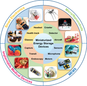
Figure 1. Integration and application of MESDs in various micro/nanosystems.
Download figure:
Standard image High-resolution imageBased on the methods of storing energy, MESDs mainly include classic microbatteries (MBs), microsupercapacitors (MSCs), and newly developed microhybrid metal ion capacitors (MHMICs) [11–16]. In particular, the compact size of MESDs with compatible performance and the capability of satisfying extreme customization requirements, such as achieving high output voltage (in series), high output current (in parallel), and high output power (multiple series), makes them preferable for powering miniaturized, flexible/wearable electronics and integrated micro/nanosystems [17–24]. In addition, easy integration with specific microelectronic devices on a compliant substrate makes MESDs the most suitable candidate for a power supply with an irreplaceable position as energy storage components for miniaturized electronic devices and integrated microsystem applications [9, 18, 25]. Figure 2 shows the sharp growth in the number of publications concerning MESDs (MBs, MSCs, and MHMICs) over the last decade (2010–2019), which is indicative of their ever-increasing importance to miniaturized energy storage systems and the necessity for further in-depth research.
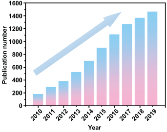
Figure 2. Statistical analysis of the number of research publications related to MESDs over the last decade (Web of Science using the key words of microbattery, microsupercapacitor, and microhybrid capacitor).
Download figure:
Standard image High-resolution imageUnlike conventional energy storage devices, MESDs are expected to be compact, versatile, smart, integrative, flexible, and compatible with various functional electronic devices and integrated microsystems [26–28]. Although the number of research articles on the topic of miniaturized/micro energy storage devices is increasing each year, a clear definition of what types of energy storage components (e.g. MBs, MSCs, and MHMICs) are considered to be genuine MESDs is still lacking. As a general rule, the total footprint area of MESDs is typically around a millimeter or centimeter, thus the thickness of microelectrodes tends to be smaller than 10 µm; the interdigitated microelectrode arrays are of micron-scale size or greater than or equal to two orders of magnitude; or the three-dimensional (3D) devices have dimensions of 1–10 mm3, including the entire part and relevant packaging [29–32]. In addition, it is worth noting that a few nonconventional energy storage devices with freestanding thin-film, wire-shaped, paper-based microelectrodes [33–36] and promising metal-air and metal-organic batteries with potential integration applications [37–39] are also included in this general definition. In our review, the term MESD mainly refers to a miniaturized energy storage system consisting of two symmetric or asymmetric microelectrodes (cathode and anode, or positive and negative electrode) with as-defined dimensions and placed on a substrate. More importantly, most of the reported MESDs have the potential to be directly integrated with micro/nanoactuators on micro/nanosystems to meet extremely integrated demands.
A number of reviews related to miniaturized energy storage have focused on material preparation, structure design, electrode fabrication strategy, functionalization, and the future challenges associated with the miniature batteries and supercapacitors [40–48]. However, a wide-ranging survey from the early design to latter target-oriented electrode manufacturing and the integrated application of MESDs including the miniaturization of batteries, supercapacitors, and hybrid metal ion capacitors (HMICs), is still highly desirable. In this review, we provide a comprehensive summary that includes configuration design, microelectrode manufacturing, and material processing, as well as typical applications of MESDs (figure 3). In addition, we also discuss on-chip integrated microsystems consisting of MESDs and a collection of practical microelectronic devices. At the end of this review, the challenges involved in the research of MESDs are discussed, including the prospects of better realizing practical applications of integrated and monolithic electronic devices in the future.
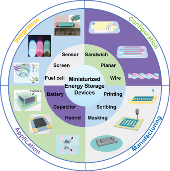
Figure 3. Illustration of the review of MESDs: configuration design, microelectrode manufacturing, typical applications, and on-chip integrated microsystems.
Download figure:
Standard image High-resolution image2. Configuration design
The device configuration has a great impact on the overall performance of an electrochemical energy storage device and leads to diverse applications based on actual conditions. In addition, extreme application requirements also promote the integration of varied morphologies and extreme manufacturing technologies. With regard to the application scenario and recent studies of MESDs, their configuration design can basically be classified into five types:
- (a)Two-dimensional (2D) stacked microdevices. As shown in figure 4(a), 2D stacked microdevices typically consist of multilayer structures with a planar substrate, a bottom current collector, anode, electrolyte, separator, cathode, and a top current collector fabricated vertically through a layer-by-layer manufacturing process [49].
- (b)
- (c)Two-dimensional arbitrary-shaped microdevices. These microdevices (e.g. Chinese traditional Tai Chi [50]), which are similar to the 2D planar interdigital microdevices but are usually fabricated using a self-made mask with filtration or printing technique, have a customizable appearance compared to conventional energy devices (figure 4(c)) [51].
- (d)Three-dimensional (3D) planar microdevices. Different from the 2D planar microelectrodes, 3D planar microelectrodes generally consist of vertically aligned, isolated perpendicular pillars, creating interdigital cathodes and anodes of 3D planar microdevices on the current collector [8]. Benefiting from the structural superiority of 3D architectures, the 3D microelectrodes are projected to boost the energy density per unit area with a highly increased loading amount of active ingredients (figure 4(d)) [52].
- (e)Wire-shaped (normally seen as one-dimensional (1D)) microdevices. In particular, the ever-increasing development of wearable electronics and integrated microsystems is boosting the demand for MESDs. The wire-shaped microdevices with intrinsically omnidirectional flexibility and the potential for extreme applications have received growing attention in recent research [53–56]. Generally, the wire-shaped microdevices can be roughly categorized into cable-shaped microdevices and coaxial-fiber-shaped microdevices, merged as the fifth type of MESD (figures 4(e) and (f)).
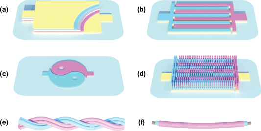
Figure 4. Schematic of the typical types of MESDs. (a) 2D stacked microdevices. (b) 2D planar interdigital microdevices. (c) 2D arbitrary-shaped microdevices. (d) 3D planar microdevices. Wire-shaped microdevices: (e) cable-shaped microdevices and (f) coaxial-fiber-shaped microdevices.
Download figure:
Standard image High-resolution imageNormally, since the overall area/volume of MESDs is comparatively miniature in size and the mass loading of active materials is usually negligible and inconvenient to measure accurately due to the varying configurations, the energy and power density of microdevices are typically expressed in μ mA−1 h cm−2 (μ mA−1 h cm−3) and μ mW−1 h cm−2 (μ mW−1 h cm−3). In particular, it should be noted that the classification of MESDs may be diverse from different perspectives. This review primarily bases the classification on the pattern distributions and functional orientation of microelectrodes.
3. Microelectrode manufacturing
Currently, the majority of MESDs are fabricated only in the laboratory, which is a long way from realizing a commercial application. In fact, the cost, reliability, efficiency, safety, etc, of microelectrode manufacturing technologies and the comprehensive properties of MESDs have a strong influence on their successful application as components of extreme application scenarios or commercial electronic products. Up to now, various advanced manufacturing technologies, including 3D printing [57], inkjet printing [58], screen printing [59], transfer printing [60], mask-assisted filtration [61], photolithography [62], electrodeposition [63], and laser scribing [64, 65], have been extensively applied to prepare desirable microelectrodes for MESDs (figure 5). Fabricating a high-resolution structure for the positive and negative microelectrodes is the main challenge to be met to achieve a high-performance MESDs under varied conditions. Diminishing the interspace is beneficial to decrease the ion diffusion pathway and the contribution of equivalent series resistance, which was demonstrated by Pech et al [66].
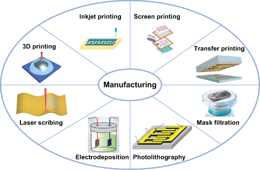
Figure 5. Advanced manufacturing technologies for the microelectrode of MESDs. 3D printing. Reproduced with permission from [57]. Copyright (2016), American Chemical Society. Inkjet printing. Reprinted from [58], Copyright (2018), with permission from Elsevier. Screen printing. Reproduced from [59]. © IOP Publishing Ltd. CC BY 3.0. Transfer printing. [60] John Wiley & Sons. © 2019 WILEY-VCH Verlag GmbH & Co. KGaA, Weinheim. Mask filtration. Reproduced with permission from [61]. Copyright (2018), American Chemical Society. Photolithography. From [62]. Reprinted with permission from AAAS. © 2010, American Association for the Advancement of Science. Electrodeposition. [63] John Wiley & Sons. © 2019, WILEY-VCH Verlag GmbH & Co. KGaA, Weinheim. Laser scribing. [64] John Wiley & Sons. © 2018 WILEY-VCH Verlag GmbH & Co. KGaA, Weinheim.
Download figure:
Standard image High-resolution imageThree-dimensional printing, academically known as additive manufacturing, refers to a class of processes (e.g. material extrusion, binder jetting, photopolymerization, and powder bed fusion) for fabricating 3D-structured objects using a layer-by-layer method. In comparison with the conventional material removal for 3D structures, 3D printing can build an arbitrarily complicated configuration without material waste; and it has shown excellent potential in the field of microelectronic devices and microsystems.
Inkjet printing is a type of computer printing that re-creates digital images by propelling droplets of ink onto various substrates. The benefits of Inkjet printing are that it is mask free and there is no contact and no material waste during the process. Despite all that, preparing stable and suitable ink for smooth printing without blocking is the critical issue. Key challenges of inkjet printing that concern researchers are mainly focused on droplet formation and morphology optimization of printed patterns.
Different from the noncontact process of 3D printing and inkjet printing, screen printing is a widely researched contact process achieved by pressing the stable and conductive ink of active electrode materials with adequate pressure to penetrate onto the prepared substrate through a customized stencil screen. Large-scale design can be realized in a short time due to its simplicity, high efficiency, and mass production technique, which reveals great promise in series-parallel microelectronic devices.
The transfer printing process involves first patterning the ink onto an intermedia (normally a stamp made up of polymers) and then transferring the ink to the premeditated substrate with appropriate force or heat. Notably, the fabrication process and final formation process are completed separately, which is promising for achieving flexible, stretchable integrated microsystems.
Mask-assisted filtration is another method developed for fabricating microelectrodes. In this process, the patterning and vacuum filtration of the electrodes designed are achieved with a mask in one step; and the mask can be used repeatedly almost without any damage. It is a simple, low-cost, and efficient technology for scalable production; but it lacks high resolution due to the size limits of masks.
Photolithography is a mature manufacturing technique that transfers the graphics of the photomask to a light-sensitive photoresist on the substrate under ultraviolet (UV) irradiation, which is widely applied in the current MEMS industry and microelectronics applications. The greatest strengths of photolithography are its high resolution and high precision, but it needs an ultraclean working environment and it is relatively time-consuming due to the complicated process.
Electrodeposition or electroplating is another cost-effective and well-controlled method that consists of applying a potential between a conductive surface and a counter electrode in the electroplating solution, where the redox-reaction is effectuated and the active material is obtained on the current collector. Since various kinds of materials (metallic anodes and polymer/metallic oxide cathodes) can be deposited and the key parameters (current, potential, plating time, etc) can be precisely controlled, electrodeposition has emerged as an essential manufacturing technology for the realization of microelectronics. What is also worth noticing is that most electrodes of wire-shaped microdevices are existing fibers or wires, which are typically loaded with active materials by further electrodeposition.
Laser scribing is a highly efficient, scalable, one-step process for fabricating microelectrodes. During the process, the interdigital architecture is obtained by ablating the active material film by laser pulse, which needs no mask or complex clean environment. The laser pulse can be directly employed to reduce graphene oxide and pattern the microelectrodes simultaneously.
In addition to the above-mentioned processes, researchers have also been exploring innovative and practical technologies for the development of microelectronics and microsystems. Notably, all of these microelectrode manufacturing technologies have their own merits and demerits; and they are still in the process of consistent development, resulting in more difficulties in making a selection among all of them. In a word, the indexes of cost, safety, efficiency, reliability, environmental protection, and practical application should all be taken into careful consideration before selecting a proper microfabrication technique to realize the large-scale application of MESDs.
4. Microbatteries
MBs, as the most widely studied type of MESD, possess the intrinsic characteristics of high energy density and durable operating lifetime and are regarded as the most likely candidate for miniaturized energy sources and most likely to integrate with microsystem applications [67–70]. Similar to traditional batteries, MBs consist of cathode (positive electrode), anode (negative electrode), electrolyte, and current collectors for repeated charging/discharging processes. In addition to presenting a relatively high energy density and stable voltage platform, MBs are also capable of adjusting the specific electrochemical requirements and operating temperature by varying the component part and structure design of microelectrodes under certain circumstances [71–73]. Recently, a number of research studies have been reported on designing micro/nanostructured positive and negative electrodes to improve capacity and lifespan, as well as to solve the difficulties involved in battery on-chip encapsulations [1, 74, 75]. Generally, MBs can be divided into alkali ion MBs and multivalent cation MBs based on the different valences of working cations. In the next two subsections, we summarize the recent advances in alkali ion MBs and multivalent cation MBs.
4.1. Alkali ion MBs
In recent years, a number of advanced configuration designs and electrode structure designs have been reported for alkali ion (e.g. lithium/sodium/potassium ion) MBs [76, 77]. A thin-film microbattery was developed rather early due to the accumulated research and accessible preparation processes. In 1983, Kanehori et al utilized chemical vapor deposition (CVD) and magnetron sputtering to fabricate the world's first thin-film lithium ion (Li-ion) MBs (LIMBs) by exploring titanium disulfide (TiS2) as the cathode, lithium metal as the anode, and Li3.6Si0.6P0.4O4 as the glassy solid electrolyte [78]. The LIMBs, prepared without any binder or additive, delivered a stable cycle life of 2000 cycles due to the relatively short Li-ion diffusion pathway. Afterwards, a diversity of thin-film micromanufacturing techniques (e.g. thermal evaporation, physical vapor deposition, atomic layer deposition, and sol-gel solution) were exploited for the fabrication of thin-film MBs [31, 79]. Meanwhile, various kinds of electrode materials and electrolyte candidates were also successfully developed for planar thin-film MB research [80, 81]. Rapid progress has been made; however, most thin-film MBs reported still face the challenges of achieving satisfactory power density, superior rate capability, and good flexibility. The electrode films usually possess a relatively low electrical conductivity; and the solid-state electrolytes, for safety and practicability, have inferior ionic conductivity.
To meet the urgent need for flexible miniaturized electronic devices, it is highly important to construct high-powered, miniaturized batteries with excellent mechanical stability and satisfactory energy for direct integration with flexible and wearable electronic systems. For instance, Lee et al demonstrated a bendable thin-film LIMB with a sandwich structure, assembled by exploring lithium cobalt oxide (LiCoO2) as the cathode, lithium phosphorus oxynitride (LiPON) as the electrolyte, and lithium metal as the anode via the collection of magnetron sputtering and thermal evaporation [49]. After physical delamination of the brittle mica substrate with the help of sticky tapes, the fabricated LIMB was then shifted onto a polydimethylsiloxane (PDMS) polymer sheet and capped with another PDMS sheet to improve the mechanical stability (figure 6(a)), which was beneficial to the stabilization of the flexible LIMB thanks to the cohesive property of PDMS. The fabricated LIMB presented a tiny voltage attenuation, from 4.071 V to 4.060 V, which only corresponded to 0.27% after 20 000 repeated bending tests. The excellent flexibility was also confirmed by almost no degradation of capacity under seriously repetitive deformation. Moreover, the bendable LIMB enabled the integration of an all-in-one, flexible, organic light-emitting diode (LED) display and energy source, rendering a pioneering idea for the progressive development of flexible electronic systems and integrated miniaturized device applications. It is worth noting that this use of a bendable thin-film microbattery was the first time a fully functionalized electronic system was fabricated with all flexible components, and it opened up a new avenue for flexible microsystem applications.
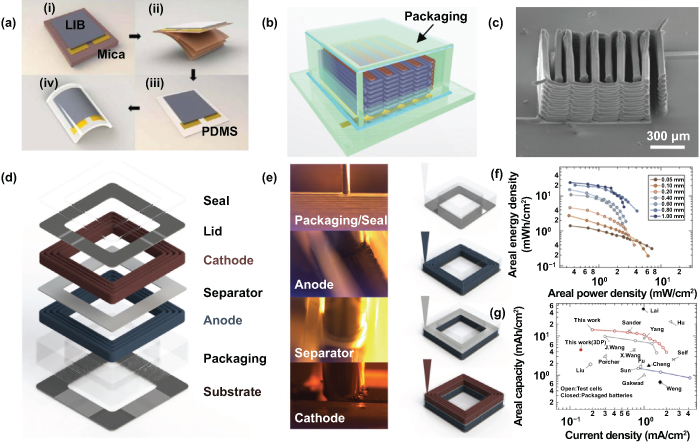
Figure 6. Alkali ion microbatteries-LIMBs. (a) Schematic illustration of the process for fabricating a flexible LIMB on a mica substrate. Reproduced with permission from [49]. Copyright (2012), American Chemical Society. (b) Polymethyl methacrylate (PMMA) packaging of 3D interdigitated microbattery. (c) Scanning electron microscopy (SEM) image of 16-layered interdigital electrode architectures. [85] John Wiley & Sons. © 2013 WILEY-VCH Verlag GmbH & Co. KGaA, Weinheim. (d) Schematic representation (expanded view) of fully 3D-printed LIMBs. (e) Images (left) and schematics (right) of direct writing of four functional inks (cathode, anode, separator, and packaging). (f) Areal energy densities and areal power densities with different electrode thicknesses. (g) Ragone plot comparing areal capacity versus current density. [86] John Wiley & Sons. © 2018 WILEY-VCH Verlag GmbH & Co. KGaA, Weinheim.
Download figure:
Standard image High-resolution imageIn addition, most publications concerning high-performance batteries focus on either cathode or anode half-cells; and they usually show improved power density at the expense of energy density. Recently, 3D microelectrodes with thicker layers have been proven to be an extremely promising design for achieving MESDs with superior power density as well as high energy density on a defined footprint. Pikul et al reported high-powered LIMBs consisting of interdigital, 3D bicontinuous electrodes with a nanoporous structure (nickel tin (NiSn) as the anode and lithium ion manganese oxide (LiMnO2) as the cathode), which provided a high power density of 7.4 mW cm−2 μm−1 and an excellent energy density of 15 μW h cm−2 μm−1 [82]. The as-fabricated 3D LIMBs equaled, or even surpassed, most supercapacitors at almost 2000 times higher than other reported microbatteries at that time.
In consideration of the great advantages of 3D electrodes and the controllable fabrication process, 3D printing has recently shown enormous potential for designing unique 3D-structured MESDs with exceptional areal/volumetric performance due to its rapid development, low economic cost, high efficiency, and scalability [83, 84]. As early as 2013, Lewis group utilized the high aspect ratio Li4Ti5O12 (LTO for the anode) and LiFePO4 (lithium iron phosphate (LFP) for the cathode) to fabricate a novel 3D LIMB by 3D printing [85]. The interdigital current collectors were patterned on the glass substrate, and then these self-made inks were precisely printed through a cylindrical nozzle of 30 µm. A calcination treatment followed, the interdigitated electrodes were filled with lithium perchlorate (LiClO4) nonaqueous liquid electrolyte, and the electrodes were sealed with a thin-layer of poly (methyl methacrylate) (PMMA) by laser cutting (figure 6(b)). These stacked interdigital electrodes were accurately achieved by a layer-by-layer printing order, and the scanning electron microscopy (SEM) image in figure 6(c) shows a 16-layer interdigital electrode architecture. As a result, the 3D-printed LIMBs presented a superior areal energy density of 9.7 J cm−2 when tested at a power density of 2.7 mW cm−2. The 3D-printed LIMBs, with full utilization of the limited space available, may open up a new research field in the application of diverse microsystems and miniaturized energy supply devices. Furthermore, the ever-growing demand for lithium-ion batteries (LIBs) with greater electrochemical performance in extremely customized structures underscores the demand for novel electrode materials, architecture designs, and assembly methods.
Rational design and efficient fabrication of 3D-printed LIMBs made up of thick microelectrodes with higher areal/volumetric capacity are necessary for the development and application of MESDs. Lewis et al recently demonstrated a new generation of 3D-printed LIMBs consisting of biphasic semisolid LFP cathode and LTO anode electrodes in customized forms by using the direct ink writing technique [86]. In addition to the LFP cathode and the LTO anode, the inks for packaging and the separator are also made up of ceramic-filled polymer composites, which are based on UV curable materials. Taken together, the 3D-printed LIMBs with thick and arbitrary-shaped electrodes were fabricated by these four semisolid inks. Then, these electrodes were further packaged by two laser-cut, glassy carbon current collectors between the top and bottom (figures 6(d) and (e)). Moreover, the areal energy densities and areal power densities of the 3D-printed LIMBs with varying electrode thicknesses from 50 µm (commercial LIBs) to 1 mm (thick LIBs) were also investigated. The results revealed that the customized LIMBs exhibited superior areal energy density and still retained high areal power density with thin electrodes (figure 6(f)). In addition, taking the entirely occupied area of the LIMBs into proper consideration, the fully 3D-printed LIMBs retained a high areal capacity of 4.45 mA h cm−2 (2nd cycle) at 0.14 mA cm−2. The Ragone plot in figure 6(g) shows that the 3D-printed LIMBs and 1 mm-thickness full cell are more favorable than other previously reported coin, Swagelok, and beaker cells. The proposed idea of fabricating high-powered LIMBs with arbitrary-shaped structures can open up new territories for customized electronic devices, sensors and actuators, and related microsystem applications with special needs. Moreover, the customizable LIMBs and developing MESDs are more likely to directly integrate with electronic objects to make up a target microsystem through printing technology, such as future electronic accessories and wearable watchbands.
As we all know, potassium ion batteries (PIBs) and sodium ion batteries (SIBs), as the next generation of alkaline ion batteries, have been seen as promising alternatives for energy storage systems on a large scale, with properties that include similar ionicity, electronegativity, and electrochemical reactivity, the same as LIBs but with earth abundance and lower cost [87, 88]. However, the larger size and different bonding characteristics of potassium and sodium ions have a great impact on the thermodynamic and kinetic properties, which can result in unknown electrochemical behavior in terms of the reaction mechanisms [89–92]. Compared with the comprehensive microscale research on LIBs, research on the miniaturization of SIBs and PIBs is still in the nascent stages. Although LIMBs possess the advantages of superior gravimetric and high volumetric energy, the potential safety hazards associated with poisonous and flammable organic electrolytes and their inferior rate performance and stability seriously hinder practical applications in the miniaturization of electronic devices. Hence, exploration of advanced candidates for energy storage systems that combine alkaline-based capacity and safe, water-based electrolytes for the multilateral needs of microsystem applications is urgently needed.
Considering the distinctive advantages of the smallest hydrated radii and the highest conductivity of potassium ions in aqueous electrolytes [93, 94], aqueous potassium ion microbatteries (PIMBs) have been determined to have great potential as highly safe MESDs that possess high-density energy with a fast charging/discharging process. However, the development of PIMBs is still hindered by the advanced materials for cathodes and anodes because of their relatively low capacity and unsatisfactory rate performance.
Li et al demonstrated the amorphous/crystalline, dual-phased, layered potassium vanadium oxide (ac-KxV2O5) as a potential anode for newly developed aqueous PIBs [95], which were obtained and placed on interdigitated 3D nanoporous gold (Au) current collectors (figure 7(a)). The corresponding high-resolution transmission electron microscope (HRTEM) image in figure 7(b) reveals the apparent crystalline and amorphous fast Fourier transform (FFT) patterns (inset images of figure 7(b)), which convincingly proved the distinct dual-phase nanostructure of amorphous nanodomains and crystalline o-V2O5 matrix. When the secondary bound interlayer of water was removed, the prepared dual-phase, nanostructured KxV2O5 · nH2O still remained as a large interlayer spacing, which was beneficial to more adequate channels and accommodation sites for potassium ion hydrating. The optimal design of a dual-phase nanostructure is able to facilitate the accessibility and transport of hydrated potassium ions and thus significantly improve the actual performance, such as enhanced capacity and rate capability.
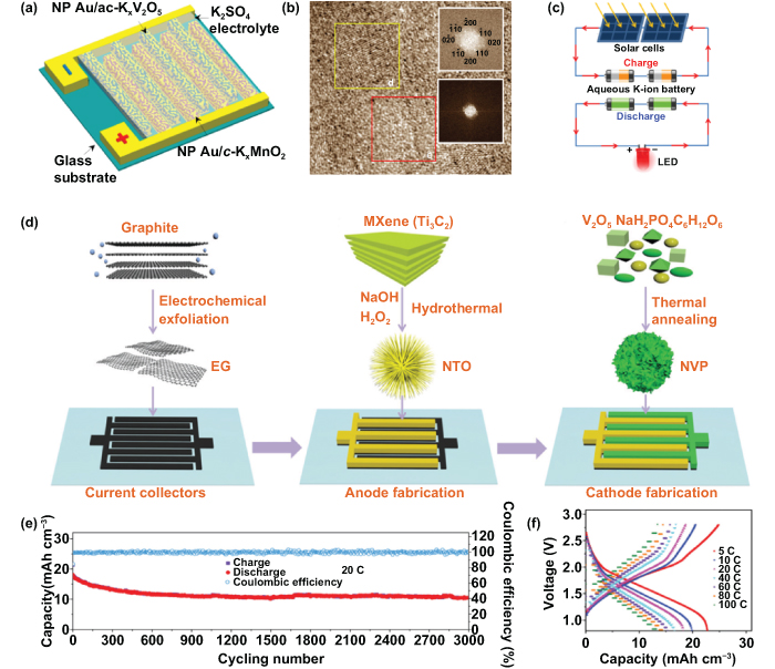
Figure 7. Alkali ion microbatteries- potassium ion microbatteries (PIMBs) and sodium ion microbatteries (SIMBs). (a) Schematic illustration of aqueous PIMBs on interdigitated nanoporous gold current collectors. (b) High-resolution transmission electron microscopy (HRTEM) image of the layered KxV2O5 with a dual-phase nanostructure; inset images are fast Fourier transform (FFT) patterns of layered KxV2O5 with crystalline and amorphous region. (c) Schematic showing a self-powered system constructed with 2 V thin-film solar cells, two-series flexible PIMBs, and LED lights. Reproduced with permission from [95]. Copyright © 2019, Springer Nature. (d) Schematic of highly conductive exfoliated graphene (EG), niobium titanium oxide (NTO) anode, and sodium vanadate phosphate (NVP) cathode. (e) Long-term cycling test of NTO|NaBF4-IE|NVP. (f) Galvanostatic charge/discharge (GCD) curves obtained at current densities from 5 to 100 C at 100 °C. Reproduced from [98], with permission from The Royal Society of Chemistry.
Download figure:
Standard image High-resolution imageTo meet the specific electrochemical requirements for portable or wearable electronic equipment, the as-fabricated PIMBs were subsequently assembled with a polyvinyl alcohol (PVA)/potassium chloride (KCl) gel electrolyte and then shifted onto a PMMA substrate. Consequently, the 3D nanoporous ac-KxV2O5 exhibited a high volumetric capacity of approximately 715 mA h cm−3 and an excellent rate performance. Moreover, the PIMBs in series and in parallel were further developed to raise the output voltage and to increase the stored energy. For practical application, the 2 V thin-film solar cells and the two PIMBs devices in series formed a self-powered system, where the energy source was from sustainable sunlight; and the LED light was powered by the stored energy from two PIMBs devices (figure 7(c)). The superior electrochemical performance of miniaturized devices makes the PIMBs promising candidates for MESDs to replenish other miniaturized energy harvest/conversion devices and to integrate with related microsystem applications.
In addition to the research on LIMBs and PIMBs, sodium ions with a larger size than lithium ions are more likely to form weakly solvated ion clusters in aprotic solvent, which contributes to a more conductive and more viable alternative for high-performance MESDs [96, 97]. Yet the research on the reasonable construction of high-powered planar sodium ion microbatteries (SIMBs) is rarely reported because there is still a lack of an effectual conductive network for ion diffusion and electron transport in advanced electrolytes.
Zheng et al were the first to fabricate a planar interdigital SIMB with a highly conductive network [98]. As shown in figure 7(d), this nonaqueous SIMB was composed of the urchin-like sodium titanate (NTO) as an anode and the flower-like sodium vanadate phosphate (NVP) as a cathode, with excellent ionic conductivity. The anode and cathode were both based on 3D highly conductive graphene nanosheets. Therefore, the metal-free current collector engineered cathode microelectrode and anode microelectrode showed superior electrical conductivity of 180 and 160 S cm−1, respectively. Meanwhile, the advanced sodium tetrafluoroborate (NaBF4)-based ionogel electrolyte reached a high ionic conductivity of 8.1 mS cm−1, which could even compete with the aqueous gel electrolyte. Benefiting from the synergetic merits of the advanced interdigital structure, the dominant multidirectional diffusion paths for sodium ions, and the contribution from pseudocapacitive (PC) characteristics (b value of 0.85), the assembled quasi-solid-state planar SIMBs displayed a long-term cyclic stability and still remained over 10 mA h cm−3 after 3000 cycles under 20 °C (figure 7(e)), which corresponded to about a 0.01% decrease every cycle. Notably, even when tested at the high temperature of 100 °C and at various current densities, the galvanostatic charge/discharge (GCD) curves showed an electrochemical property similar to that under room temperature and delivered a surprising capacity of 13.5 mA h cm−3 under the superhigh rate of 100 C (figure 7(f)). This work shows that reasonably designing the conductive network for microelectrodes and fully exploiting the mechanism of multiway ion diffusion can improve the power density and energy density of miniaturized batteries concurrently, manifesting a lot of potential for high-demand microelectronics and microsystem applications. Furthermore, the proposed type of MESD is believed to be the idealized design for basic research of the charge/discharge mechanism through in situ characterization.
4.2. Multivalent cation MBs
In the above-mentioned alkali ion MBs, alkaline metals, such as lithium (Li), sodium (Na), and potassium (K), are awfully easy to react; and their associated organic electrolytes are noxious and flammable, which always leads to massive safety and health risks [99–101]. In other aspects, a lack of alkaline metal resources, especially lithium, and the unevenly distributed metal resources on the planet has led to a high cost for alkali ion batteries and their miniaturization.
Against this background, the mechanism of multivalent cation energy storage has been proposed and increasingly utilized in recent years to design and fabricate new-fashioned energy storage devices [102, 103]. Different from the batteries on the basis of the alkali ion (e.g. lithium/sodium/potassium ion), multivalent cation (e.g. zinc/magnesium/aluminium ion) batteries have the distinctive advantages of high capacity density, high energy density, and fast charge transfer dynamics. As a result, an increasing wave of research on multivalent cation batteries is occurring, as well as on multivalent cation MBs, such as zinc ion MBs (ZIMBs), magnesium ion MBs (MIMBs), and so on. Furthermore, the multivalent cation-based devices are less sensitive to air and water so they are preferable for practical, large-scale applications and work under extreme outdoor environments. Among all multivalent cation batteries, the zinc ion batteries (ZIBs) have gained especially wide attention due to their inherent advantages of high security, low cost, and environmental protection [104–106]. In general, the ZIBs are made up of a zinc (Zn) metal anode, an aqueous electrolyte containing Zn2+, and a layered or tunnel-structured material for a Zn2+ intercalation/deintercalation cathode [107, 108]. In contrast to the reaction between air and alkaline metal electrodes, metallic Zn shows high stability in the natural environment and is highly abundant on the earth, making it an ideal anode for aqueous batteries. What's more, metallic Zn possesses a relatively low redox potential; and the two-electron redox reaction also contributes to the wide application of Zn-based energy storage devices. Diverse kinds of Zn-based batteries have been reported, such as zinc-nickel (Zn-Ni) [109], zinc-manganese (Zn-Mn) [110], and zinc-vanadium (Zn-V) [111] batteries. However, the unsatisfactory cycling stability stemming from the dendritic growth of a Zn anode still impedes the development of ZIBs and their miniaturization. In addition, few works have been reported to realize fully flexible/wearable and miniature Zn-based energy storage systems; and the study on inhibiting the growth of zinc dendrite in miniaturized devices is still in a deficient stage.
Recently, Liu et al reported the patterned conductive metal films and planar ZIMBs on a textile substrate using a novel resist dyeing process [112]. Using this resist dyeing process and subsequent electroless/electrodeposition, the wavy fabric was converted into arbitrary conductive patterned cloth and different colors, which indicates it has a promising future for applications in textile-based MESDs. Various materials, such as copper (Cu), Zn, and nickel-cobalt (Ni-Co) bimetallic oxyhydroxide (NiCo BOH) can be electrodeposited on the surface of a conductive Ni pattern (flowers), as shown in figure 8(a). The ZIMBs were fabricated by forming electrodeposited Zn and NiCo BOH on conductive Ni films (only the sensitized area was deposited), and the sealed area was left as an insulating gap. Subsequently, a PVA gel electrolyte was coated on interdigital textile electrodes. Impressively, the textile-based Zn anode significantly suppressed dendrite growth and showed cyclic stability and reversibility superior to that of the Zn foil, profiting from the naturally porous fabrics and uniform electroplated Zn nanosheets.
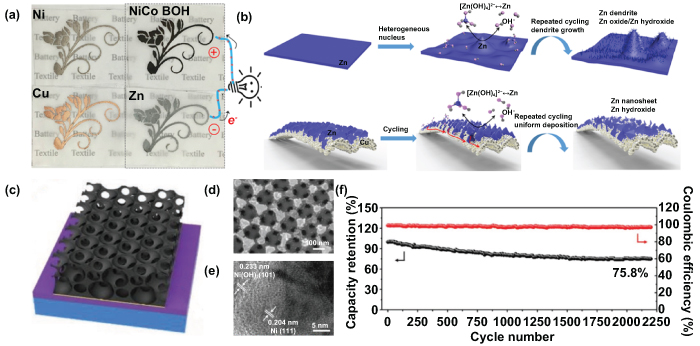
Figure 8. Multivalent cation microbatteries. (a) Photograph of flowers fabricated on polyester fabrics with different coatings (Ni, Cu, Zn, and NiCo BOH). (b) The morphology evolution of Zn foil and Zn textile during cycling. Reproduced with permission from [112]. Copyright (2019) American Chemical Society. (c) Schematic of hierarchical ordered porous (HOP) nickel@nickel hydroxide (Ni@Ni(OH)2) microelectrode. (d) SEM image and (e) HRTEM image of the HOP Ni@Ni(OH)2 microelectrode. (f) Long-term cycling performance and corresponding coulombic efficiency of the HOP Ni@Ni(OH)2 microelectrode. [115] John Wiley & Sons. © 2019 WILEY-VCH Verlag GmbH & Co. KGaA, Weinheim.
Download figure:
Standard image High-resolution imageThe morphology evolution of flat Zn foil and electroplated Zn nanosheets during the cycling process is illustrated in figure 8(b). The flat Zn foil electrode showed obvious pulverization of Zn and heterogeneous dendrite growth, while the Zn nanosheets deposited on the porous fabrics could provide larger active surface areas. The Zn2+ was preferable for electrodeposition on the surface of an ultrathin nanosheet during the charging process. Moreover, electroplated Zn nanosheets with higher density were more likely to obtain a dispersed electric field concentration, thus the electric field would be relatively uniform, rather than a strong enhancement of the electric field, which is beneficial for improving the cycling stability, reversibility, and effectively suppressing dendrite growth. Combining the advantages of resist dyeing technology and electroless/electrodeposition with minimal sacrifice in the flexibility of fabrics, this work presents a new potential for obtaining a flexible, textile-based MESD with aesthetic design versatility and high rechargeability. It shows much promise for powering wearable electronic devices and subsequent integration with microsystem applications.
In most investigations of multivalent cation MBs, the coalition of high energy density and high rate performance is desperately needed. Increasing the thickness of microelectrodes has been proven to increase the mass loading of active materials and to acquire a higher areal/volumetric energy density of the energy storage device. Nevertheless, thicker electrodes cannot avoid declined power density or inferior rate capability because of their longer electron and ion diffusion distances.
Recently, designing 3D micro/nanostructured microelectrodes has been seen as an efficient way to realize a high energy/power density and excellent rate capability in a confined size. In comparison to 2D microelectrodes, 3D mesostructured microelectrodes possess a higher specific surface area, the characteristics of a short ion transport distance, and high-efficiency electron diffusion paths, making them more promising candidates for high-powered MESDs [113, 114].
To realize high-performance multivalent cation MBs based on a 3D micro/nanostructure, Hao et al designed a quasi-solid-state Ni-Zn microbattery on hierarchically ordered porous (HOP) Ni@Ni(OH)2 microelectrodes, displayed in figure 8(c) [115]. The as-prepared microelectrode possesses a core–shell structure with a HOP Ni skeleton (core) and Ni(OH)2 (shell). Due to the interconnected and highly conductive network, the as-fabricated microelectrode proved to optimize the ion and electron transport simultaneously (see the SEM and HRTEM images shown in figures 8(d) and (e)). More importantly, when the thickness of the HOP Ni@Ni(OH)2 microelectrodes increased, the corresponding areal energy density also ascended almost proportionally, while the areal power density only decreased in a tiny wastage. As a consequence, the HOP Ni@Ni(OH)2–5.6 microelectrode with the greatest electrode thickness, 5.6 μm, was further tested to study the cycling stability, which retained 75.8% of initial capacity and achieved nearly 99.9% coulombic efficiency (CE) after 2200 cycles at 20 mA cm−2 (figure 8(f)). Moreover, the ZIMBs exhibited a remarkable energy density (0.26 mW h cm−2, 0.12 W h cm−3) and power density (33.8 mW cm−2, 15.8 W cm−3), surpassing the majority of recent miniaturization research on energy storage devices. Given the success of achieving both excellent energy density and superior power density for MESDs, this advance may shed light on a new research direction in high-performance, highly safe, miniaturized energy storage units for the next generation of integrated microsystem applications.
Building highly durable, flexible, wearable, and deformable energy storage devices with satisfactory electrochemical properties and shape versatility is another big challenge in the research field of MESDs [116, 117]. These specific demands can be solved by 1D fiber or wire-shaped energy storage devices thanks to their superlight weight, compact size, and diverse structures [118, 119]. In addition, wire-shaped energy storage devices are easier to integrate with commercial textile fabrics, making them preferable candidates for smart electronics and deformable microsystems, particularly for the wearable, textile-based applications [120]. Viewed from the practical use of wearable electronics, wire-shaped energy storage devices are expected to hold high energy capacity and to maintain their electrochemical performance even under extremely challenging conditions (bent, stretched, cut, and washed).
To realize a highly flexible and stretchable energy device, Li et al developed the waterproof, tailorable, and stretchable yarn ZIMBs by employing double-helix yarn electrodes and the superior cross-linked polyacrylamide (PAM) electrolyte (figure 9(a)) [121]. The double-helix carbon nanotube (CNT) yarns worked as a substrate for a manganese oxide (MnO2) cathode and a zinc anode, which could provide enhanced strength for microelectrodes under various deformation states. What is more, the yarn microelectrodes also significantly improved electrolyte wetting of the electrode surface. Compared with the widely used PVA-based gel electrolytes, which always face the challenges of low ionic conductivity and poor elasticity, the late-model hydrogels are believed to dissolve multiple kinds of ions and are seen as promising good ionic conductors because the hydrophilic polymer networks are swollen with a copious amount of water [122]. For this PAM-based electrolyte of yarn ZIMBs, the PAM chains network was achieved by covalent cross-links and hydrogen bonds; and the cross-linked PAM hydrogel was obtained by heating it at 50 °C for 4 h using a free-radical polymerization approach (figure 9(b)). Furthermore, the yarn ZIMBs were tested in a continuous deformation to estimate their durability and stability. The as-prepared ZIMBs still retained a capacity retention of over 95% after being bent, knotted, and twisted in sequence (figure 9(c)). Even after being strained to 300% of the initial state, they still retained a high capacity retention of 94.8% after 100 cycles, as shown in figure 9(d). The excellent strength and high electrochemical stability of the yarn ZIMBs with PAM-based electrolyte under various deformation conditions may open up a path to new, promising, and reliable MESDs for wearable electronic devices and flexible microsystem applications.
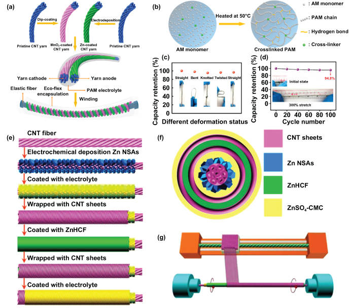
Figure 9. Wire-shaped multivalent cation microbatteries. (a) Schematic diagram of fabrication and encapsulation of yarn ZIMBs. (b) Schematic diagram for the fabrication of cross-linked polyacrylamide (PAM)-based electrolyte. (c) Capacity retention of the yarn ZIMBs under various deformation status. (d) Dependence of capacity retention on cycle numbers with a strain of 300%. Reproduced with permission from [121]. Copyright (2018) American Chemical Society. (e) Schematic illustrations showing the fabrication process of the coaxial fiber ZIMBs. (f) Schematic illustration of the cross-section of the ZIMBs. (g) Wrapping aligned CNT sheets around the modified CNT fiber. Reproduced with permission from [54]. Copyright (2019) American Chemical Society.
Download figure:
Standard image High-resolution imageUnlike the twin-fiber (cable-shaped) structure described earlier, the design of a single coaxial fiber structure can offer a simple and effective means of developing ultraflexible, deformable, and high-powered MESDs [123]. Although there are plenty of material options available for coaxial fiber MESDs, developing eco-friendly and fiber-shaped MESDs on one single fiber with the required electrochemical performance and long cyclic ability is still a challenging task for researchers. Zhang et al demonstrated flexible, coaxial fiber, aqueous rechargeable ZIMBs by employing Zn nanosheets as the inner electrode and zinc hexacyanoferrate (ZnHCF) composite as the outer electrode (figure 9(e)) [54]. It should be noted that the Zn electrode and ZnHCF composite was based on the CNT fiber and aligned CNT sheets, respectively.
The uniquely designed structure of coaxial fiber ZIMBs possessed multiple advantages, such as a larger surface area, smaller contact resistance of the coaxial structure, alignment of the charge transport paths, excellent mechanical stability, and stable electrochemical properties after a long bending time. Figure 9(f) is a schematic of a cross-sectional structure of coaxial fiber ZIMBs. The aligned structure demonstrated a fast charge transport, and the unique coaxial structure made the greatest utilization of the effective surface area between the cathode and anode. Through the exceptional design shown in figure 9(g), the aligned CNT sheets were easily wrapped around CNT fiber. In addition, two long ZIMBs were further connected in series and combined with a flexible textile to light a 3.3 V LED light, further verifying the favorable flexibility and weavability of the as-fabricated ZIMBs. The proof-of-concept demonstration of coaxial fiber ZIMBs is believed to open up new possibilities for the highly safe and economical MESD applications.
5. Microsupercapacitors
In recent years, interest in MSCs has increased as alternative miniaturized power sources with high power density, outstanding rate performance, high-frequency response, and long cycling capability [124–126]. Generally, MSCs can be classified as electric double layer capacitive (EDLC) MSCs and PC MSCs, depending on the charge storage mechanism, ion adsorption/desorption for EDLC MSCs, and the faradaic reaction for PC MSCs between the electrode and electrolyte [127–129]. Carbon and carbon-based materials have been the most widely researched and are the most likely to be commercialized materials for supercapacitors, due to their low cost, large surface area, high electrical conductivity, and controllable porosity properties [130–132]. The most extensive research on PC electrode materials is on inorganic metal compounds and conductive polymers because of their speedy reversible faradaic redox reactions [133–135]. Under normal circumstances, EDLC materials usually show superior cycle life; but they are more likely to have lower capacity compared to PC materials.
5.1. Electric double layer capacitive MSCs
EDLC MSCs typically work in a non-Faradaic process, where the capacitance relates to the ion charge/discharge between the electrode interfaces; and they store electrical energy in a directly electrostatic manner [136]. The most classic characteristic of an EDLC process is that no chemical changes are involved. During the charge process, excess and deficient electron charges on the two plates of a capacitor are established; and the ions in the electrolyte (cations and anions) are transferred to the charged interfaces through the solution [137, 138]. The EDLC-based materials, especially carbon-based materials, possess a large surface area and superior electrical property, which have attracted growing interest by researchers. The EDLC-based materials, such as active carbon [139, 140], CNTs [86, 141], graphene [142–144], carbon derived from metal carbide [145, 146], and photoresists [147, 148] are commonly used as the electrode materials of supercapacitors. In addition, creating advanced micro/nano structures with great ion diffusion has been proven to be an efficient method of enhancing the overall electrochemical performance of EDLC MSCs [129, 149]. For instance, onion-like carbon (OLC) was reported to offer a specific surface area of ∼500 m2 g−1, which is moderate compared to activated carbons [150]. What makes the OLC unique from previously reported carbon-based materials is that its surface is completely accessible to ion adsorption thanks to the non-porous network inside the particles. The cross-section of a charged OLC (grey) capacitor is shown in figure 10(a), which is composed of two layers of charges (blue and pink). The discharge rates could reach up to 200 V s−1, which is much higher (even three orders of magnitude) than the traditional supercapacitors, enabling them to compete with traditional batteries and electrochemical capacitors in numerous applications.
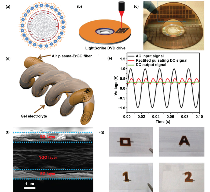
Figure 10. Electric double layer capacitive microsupercapacitors. (a) Cross-section of a charged zero-dimensional OLC (grey) capacitor. Reproduced with permission from [150]. Copyright © 2010, Springer Nature. (b) Interdigital graphene electrodes readily LightScribed on a disc. (c) More than 100 MSCs produced on a single disc. Reproduced with permission from [155]. Copyright © 2013, Springer Nature. (d) Schematic of assembled fiber-shaped MSC device. (e) AC input signal and rectified pulsating DC signal. Reproduced with permission from [144]. Copyright (2019), American Chemical Society. (f) Cross-section SEM image of layer-structured exfoliated graphene/graphene oxide/exfoliated graphene (EG/NGO/EG) film. (g) Photographs of different planar sandwich supercapacitors. Reproduced with permission from [160]. Copyright (2017) American Chemical Society.
Download figure:
Standard image High-resolution imageCompared to the commercial carbon materials, graphene has also drawn global attention for its remarkable properties, such as a super high, theoretical surface area (2630 m2 g−1), excellent electronic properties, and superior mechanical stability [151, 152]. However, conventional micromanufacturing techniques tend to be cumbersome and inefficient in preparing low-cost microdevices based on graphene, thus limiting its further widespread application.
Recently, laser direct writing has been reported to fabricate in-plane and multilayer stacked MSCs on polyimide sheets for improving areal capacitance and to transfer natural lignin into porous, conductive carbon structures and interdigitated circuits for developing green energy storage devices [153, 154]. Combining the merits of graphene and laser direct writing, El-Kady et al demonstrated a viable method of fabricating large-scale graphene MSCs by direct laser writing on graphite oxide (GO) films through a consumer-grade LightScribe DVD burner [155], as shown in figure 10(b). This process is accessible to scale up, and the devices can also be fabricated on other large substrates at a lower cost than previous microfabrication technologies. The as-produced, all-solid-state devices are extremely thin and fully flexible. More than 100 laser-scribed graphene MSCs were fabricated directly on a disc in no more than 30 min (figure 10(c)). The obtained graphene electrodes possessed distinguished merits, such as the exceptional electrical conductivity (2.35 × 10³ S m−1), a large specific surface area (1520 m2 g−1), and an open network structure. Accordingly, compared with active carbon-based supercapacitors, the as-fabricated interdigitated MSCs, with a simple and efficient method, presented a significantly improved energy/power density, offering great potential for large-scale applications of MESDs.
In the field of functional applications, graphene-based materials are regarded as the best prospective electrode materials of electrochemical capacitors for alternating current (AC) line filtering due to their outstanding electrical conductivity, chemical durability, large theoretical specific surface areas, and superior mechanical stability [156]. However, the reduced graphene oxide (rGO), which is generally obtained from graphene by a wet chemical method, imports impure components; and the resulting electroconductivity is generally lower than that of pristine graphene [157]. Consequently, producing electrode materials of rGO with high electrical conductivity using a simple method for MSCs is urgently needed.
Yao's group demonstrated the first highly electrically conductive rGO fiber-shaped MSCs using a one-step argon (Ar) plasma-engraving strategy [144]. Two twisted fibers were used to construct a symmetrical fiber-shaped MSC (figure 10(d)), and the AC line filtering tests were studied. The fiber-shaped MSCs displayed rapid frequency with a phase angle of −81.1° at 120 Hz. The filtering performance of the fiber-shaped MSCs fabricated was close to that of commercial electrolytic capacitors and even comparable to most reported graphene-based supercapacitors [158]. In addition, a functional generator delivered an AC signal (1.0 Vpeak|peak, 60 Hz); and it was successfully converted to a pulsating direct current (DC) signal by a full-bridge rectifier (figure 10(e)). Thus, the proposed graphene-based MSCs exhibit a promising future for practical application of AC line filtering and the functionalization of MESDs for various microsystem applications.
In addition to the interdigital and fiber-shaped configuration of MSCs, research on an innovative paradigm of miniaturized devices has been conducted in recent years [55, 159]. Zheng et al demonstrated a universal printing technology to prepare planar sandwich supercapacitors with arbitrary shapes [160]. The electrochemically exfoliated graphene (EG) electrodes showed a layer structure, and the graphene oxide (NGO) worked as the separator on a single substrate. A cross-section SEM image in figure 10(f) shows a clearly layered structure of EG/NGO/EG Viewing the SEM image, the thickness of the EG layers was approximately 700 nm; and they possessed a high electrical conductivity of around 50 S cm−1. Moreover, the self-designed MSCs not only possessed multiple arbitrary shapes, e.g. rectangle, hollow square, letter A, and the numbers 1 and 2 (figure 10(g)) but also demonstrated excellent electrochemical performance (∼ 280 F cm−3), outstanding flexibility (almost no capacitance degradation under various bending scenarios), and ready scalability. It is worth noting that this work firstly realized the flexible stacked MSCs with arbitrary shapes; and the proposed method can be expanded to other large-scale production of versatile-shaped, flexible electronic devices and underlying microsystems.
5.2. Pseudocapacitive MSCs
PC MSCs usually demonstrate relatively high specific capacitance and superior energy density but inferior cycling stability, as compared to EDLC MSCs. Typical EDLC-based electrode materials, such as carbon and carbon-derived materials, tend to have a comparatively lower specific capacitance. By contrast, PC MSCs based on conductive polymers, such as polythiophene, polypyrrole (PPy), and polyaniline (PANI) [161], transition metal carbides and carbonitrides (Mn +1XnTz) [134], transition metal oxides or nitrides (MxO and MxN) [128], hydroxides [162], and disulfides [163] often exhibit a higher specific capacitance due to the reversible and rapid faradaic reactions occurring on the surface of electrodes. As a consequence, PC materials have been widely utilized to construct MSCs for contributing higher specific capacitance. What should also be mentioned here is that the enhanced areal/volumetric capacitance is critical for MSCs because the footprint area of the device is a vital factor in evaluating the overall performance of MSCs. For instance, Wang et al reported an all-solid-state planar PC MSC with microelectrodes of patterned PANI nanowire arrays, which combined the top-down microfabrication technique and the bottom-up in situ chemical polymerization method [164]. In their method, they utilized a dilute polymerization process to in situ deposit the PANI nanowire arrays on the interdigital Au current collectors. The flexible PANI nanowire arrays-based MSCs acquired an exceptional volumetric capacitance of 588 F cm−3, superior rate performance, and low leakage current. Additionally, the MSCs were further connected in series or in parallel to improve the output potential or output current to meet the practical needs.
In addition to the conductive polymers, 2D transition metal carbides and carbonitrides, known as MXenes, have gained increasing interest among researchers due to their high specific capacitance, high electrical conductivity, and outstanding mechanical stabilities [165, 166]. Meanwhile, the traditional micromanufacturing technologies are usually costly and time-consuming because they tend to pattern the current collectors first and then obtain the active materials by the electroless/electrodeposition. After these routine microfabrication processes, they will unavoidably import abundant voids in the active materials, which always leads to ordinary electrochemical performance in the applications of MSCs. Contemplating all of this, constructing fast and efficient MSCs with superior areal/volumetric capacitances is a crucial requisite for the development of the PC materials, as well as MSCs and microsystem applications.
As illustrated in figure 11(a), Zhang et al revealed the quick manufacturing of flexible MSCs by combining the stamp printing technique and MXene inks (Ti3C2Tx and Ti3CNTx) [50]. Three-dimensional printing was used to fabricate the patterned stamps, and the stamps were coated with MXene inks. Finally, the active materials were transferred onto paper or other substrates by pressing firmly. To explore more capabilities of the stamp printing method, various stamp shapes were designed and fabricated. They were coated with MXene inks and firmly pressed onto paper substrates (figure 11(b)). Finally, the solid-state MXene-based MSCs were obtained when silver (Ag) wires were attached; and the PVA/sulfuric acid (H2SO4) gel electrolyte was drop-cast on the electrodes. The fabricated Ti3C2Tx MSCs exhibited an excellent areal capacitance of 61 mF cm−2 at 25 μA cm−2, coupled with high energy density, high power density, and long cycle life (figure 11(c)). Interestingly, unlike another extensively studied 2D material, graphene, which is hydrophobic and needs additional surfactant or polymer to form a stable aqueous solution, the Ti3C2Tx MXene inks exhibit an exhilarating hydrophilicity; and their electronic conductivity is also higher than the processed graphene solution. Accordingly, the proposed stamping method for fabricating MSCs is not only low cost and time-saving but is also capable of being painted or handwritten onto any hydrophilic substrates, showing great potential for next-generation applications of MESDs and integrated microsystems.
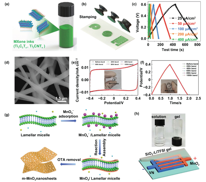
Figure 11. Pseudocapacitive microsupercapacitors. (a), (b) Stamping of the MXene inks (Ti3C2Tx, Ti3CNTx). (c) GCD profiles of the fabricated Ti3C2Tx MSCs. [50] John Wiley & Sons. © 2018 WILEY-VCH Verlag GmbH & Co. KGaA, Weinheim. [50] (d) SEM image of the nickel ferrite (NiFe2O4) after calcination. (e) Capacitance-voltage (C-V) curves and (f) GCD profiles after being bent for a different number of times. Reproduced from [167], with permission from The Royal Society of Chemistry (g) Schematic of the synthesis of m-MnO2 nanosheets. (h) Schematic of vanadium nitride (VN)//MnO2 MSCs. Insets are 5 M lithium bis (trifluoromethane sulfonyl) imide (LiTFSI) liquid electrolyte (left) and silicon dioxide (SiO2)-LiTFSI gel electrolyte (right). Reprinted from [172], Copyright (2019), with permission from Elsevier.
Download figure:
Standard image High-resolution imageMore recently, by adopting electrospinning and photolithography, Shen's group successfully synthesized porous nickel ferrite (NiFe2O4) nanofibers and fabricated the flexible all-solid-state planar MSCs [167]. Figure 11(d) shows the SEM image of the calcined sample, where we can clearly see the calcined NiFe2O4 nanofibers with a porous structure; and the average diameter of calcined nanofibers was around 200 nm. The rationally designed structure with mesopores was beneficial, providing a conductive path for ion reaction and lowering ion diffusion impedance, thereby contributing to the improved electrochemical property of the prepared planar MSCs. The cyclic voltammetry (CV) curves (at a scan rate of 1 V s−1) and GCD curves (at 10 µA cm−2) of the MSCs are presented in figures 11(e) and (f) after being bent for a different number of times (20–100). It is necessary to note that the as-fabricated MSCs can directly contact the human body and be attached to human skin, which confirms the excellent flexibility and superior mechanical stability of the planar MSCs and further reveals their great contribution to flexible and wearable electronic devices.
As for the transition metal oxides/hydroxides (TMOs/TMHs), they have been extensively studied as advanced electrode candidates due to their high theoretical capacitance, sufficient redox reactions, and chemical stability [168–170]. Nevertheless, the TMOs/TMHs materials tend to display inferior electrical conductivity and severe volume change during cycling life, leading to inferior rate capability and a short cycle life of corresponding energy storage devices. In order for TMOs/TMHs to achieve better electrochemical performance, the introduction of a mesoporous structure, combined with a high electrical conductive network, is an effective strategy for fabricating high-performance MSCs [171].
By introducing a bottom-up self-assembly strategy, Qin et al fabricated the ultrathin and mesoporous manganese dioxide (m-MnO2) nanosheets as the cathode and porous vanadium nitride (VN) nanosheets as the anode for the high-powered asymmetric MSCs (figure 11(g)) [172]. The EG nanosheets served as both current collectors and conducting additives, and the VN//MnO2 MSCs were assembled in the novel 'water-in-salt' gel electrolyte of SiO2-lithium bis (trifluoromethane sulfonyl) imide (LiTFSI) through a mask-assisted layered deposition, shown in figure 11(h). Impressively, the assembled MSCs showed a stable output of 2.0 V and displayed a high energy density of 21.6 mW h cm−3, with enhanced rate performance and prolonged cycle lifetime. The reported MSCs outperformed most of the studied MSCs with MnO2; and the obtained energy density was superior to that of lithium-based, thin-film batteries (less than 10 mW h cm−3) [173–175]. Furthermore, the all-solid-state planar MSCs presented excellent mechanical stability under various bending tests, showing significant potential for further advanced fabrication of energy storage devices with miniaturized integration for numerous microsystem applications.
6. Microhybrid metal ion capacitors
Rechargeable batteries and supercapacitors have become two kinds of indispensable electrochemical energy storage devices in consumer electronics, electric vehicles, large-scale electricity storage instruments, and so on [176–181]. Nevertheless, low power output of batteries and low energy density of supercapacitors severely limit their further potential for large-scale applications. The concept of HMICs was established and developed by combining the advantages of batteries and supercapacitors [182, 183]. A typical HMIC consists of one capacitive electrode as a power source and the other battery-type faradaic electrode as an energy source [125]. From the perspective of an energy storage mechanism, the capacitive cathode functions through an ion adsorption/desorption on the surface and the anode works via a cation insertion/extraction process. These two asymmetric charging/discharging processes for electrodes tend to work in different potentials, thereby contributing to an enlarged operating potential window in an effective way and improving the energy density of electronic devices as well [43]. Analogous to rechargeable batteries (alkali ion batteries and multivalent cation batteries, as we mentioned before), the nomenclature of HMICs is generally rooted in their internal shuttling cations and can be classified as hybrid alkali ion capacitors, such as hybrid lithium ion capacitors (HLICs), and hybrid multivalent cation capacitors, such as hybrid zinc ion capacitors (HZICs). Additionally, MHMICs combine the advantages of minute footprint devices and hybrid capacitors, thus being characterized by high energy density, high power output, and accessibility of integration in the energy storage system.
6.1. Microhybrid alkali ion capacitors
Among all of the hybrid alkali ion capacitors, lithium-based hybrid ion capacitors have attracted growing research interest and technological attention due to their high energy/power density and relatively early research on LIBs. It is well known that LIBs are the most extensively applied energy storage systems, especially in new energy electric vehicles and portable electronic devices [184, 185]. Therefore, it is no surprise that one of the earliest miniaturizations of metal ion capacitors is HLICs, which were studied and patented by Amatucci et al in 2001 [186, 187]. The assembled HLICs with a nanostructured anode (Li4Ti5O12) and cathode (activated carbon) effectively bridged the gap between LIBs and capacitors, which has gained the attention of researchers worldwide since then. However, most of the reported miniaturization of HLICs are constructed in a stacked form, with the sandwich structure of the separator or quasi-solid-state/solid-state electrolyte between the cathode and anode. In addition, most reported MESDs represent unsatisfactory mechanical flexibility, inferior high-temperature electrochemical property, and difficulty in integration with other electronic devices, which makes it hard to satisfy the growing demands of smart on-chip integrated electronic systems.
To address the aforementioned challenges, Wu's group firstly reported the planar microhybrid lithium ion capacitors (MHLICs) based on an interdigitally patterned anode of LTO nanospheres and a cathode of activated graphene (AG) [188]. They utilized a layer-by-layer deposition with masking to prepare the interdigitated MHLICs, thus the graphene and electrode materials (LTO//AG) were obtained without any polymer binders or additives (figure 12(a)). Remarkably, the designed MHLICs presented an excellent capacity retention of 98.9% after 6000 cycles; and the CE was constantly kept very close to 100% during repeated cycles (figure 12(b)). Even tested at 80 °C, the as-prepared MHLICs still maintained a surprising high-temperature stability and exhibited excellent mechanical stability under various extremely deformed conditions, without an obvious decline in electrochemical properties. Furthermore, the Ragone plot in figure 12(c) indicates that an ultrahigh volumetric energy density of 53.5 mW h cm−3 was obtained from the assembled all-solid-state MHLICs, which shows their distinct superiority to most reported lithium thin-film batteries and supercapacitors. Meanwhile, the proposed layer-by-layer deposition was easy to scale up and apply to MESDs to satisfy the specific requirements of oriented electronic systems, holding significant promise in the development of miniaturized device applications and highly integrated microsystems.
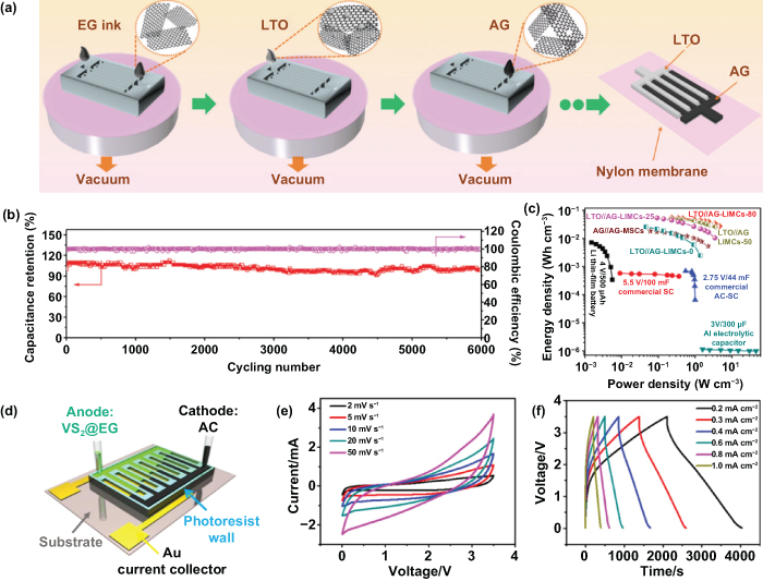
Figure 12. Microhybrid alkali ion capacitors. (a) Schematic diagram of the fabrication of LTO//AG-MHLICs by mask-assisted filtration. (b) Cycling stability measurements of MHLICs for 6000 cycles. (c) Ragone plot of all-solid-state MHLICs and other commercially available energy storage devices. Reproduced from [188], with permission from The Royal Society of Chemistry. (d) Schematic illustration of the asymmetric configuration of nonaqueous MHSICs. (e) CV curves at the scan rates of 2–50 mV s−1 from 0.01–3.5 V. (f) GCD profiles at the current densities ranging from 0.2 to 1.0 mA cm−2. [193] John Wiley & Sons. © 2019 WILEY-VCH Verlag GmbH & Co. KGaA, Weinheim.
Download figure:
Standard image High-resolution imageBesides the lithium-based hybrid ion capacitors, research on hybrid sodium ion capacitors (HSICs) has also grown rapidly in recent years. Profiting from the abundance of sodium on the earth, the low cost of sodium carbonate and sodium-based salt electrolyte, a sodium-based energy storage system has been considered to be a vital complement to the commercialized lithium-based energy storage system [189–191]. Among the emerging transitional metal dichalcogenides (TMDCs), vanadium disulfide (VS2) has attracted widespread attention in electrochemical energy storage systems because of its superior electrochemical and mechanical property [192]. However, the potential application of VS2 in SIBs and miniaturization of HSICs need to be further explored. Zhang et al constructed a novel nonaqueous microhybrid sodium ion capacitors (MHSICs) by employing vertically aligned VS2 nanosheets on electrochemically EG sheets as an anode (VS2@EG), activated carbon as a cathode, and nonaqueous sodium perchlorate (NaClO4) dispersion as electrolyte (figure 12(d)) [193]. For the reaction mechanism, the activated carbon electrode shows a typical ion adsorption/desorption and the VS2@EG electrode displays a mainly surface-controlled reaction process. Benefiting from the electrode materials and especially NaClO4-contained organic electrolyte, the as-prepared MHSICs exhibited a superior cycling stability and reversibility with a wide voltage range of 0.01–3.5 V (figure 12(e)). Furthermore, the GCD profiles under different rates and the asymmetric graphs in figure 12(f) further confirmed the exemplary PC charge storage characteristics. Based on all advantages, the MHSICs exhibited an outstanding areal capacitance of 110.7 mF cm−2 at 0.2 mA cm−2; and it reached a superior areal energy density of 188.3 μW h cm−2 at 0.35 mW cm−2, outperforming the mostly reported MSCs in recent time. Thus, this proposed MHSIC will not only promote the application of newly developed miniaturization of hybrid electronic devices but also imply a significant promise in the self-energizing microsystem applications.
6.2. Microhybrid multivalent cation capacitors
Hybrid multivalent cation capacitors are also being developed as new-generation energy storage systems and have been widely researched due to the merits of multivalent cation storage mechanisms mentioned in section 4.2, multivalent cation MBs, and the advantages of capacitors mentioned in section 5, MSCs. In general, hybrid multivalent cation capacitors include, but are not limited to, HZICs, hybrid magnesium ion capacitors (HMICs), and hybrid aluminum ion capacitors (HAICs). In particular, Zn metal electrodes possess distinct superiorities, such as high abundance, high stability, and low flammability. Taken together, Zn-based hybrid capacitors are becoming one of the best choices for next-era power supply owing to the high energy and high power density, large charge/discharge rates, and long cyclic stability [194–197]. Benefiting from the wide voltage range between Zn and activated carbon (∼1 V), they can be easily fabricated into a desirable Zn-based hybrid capacitor system. Recently, Feng's group explored the electrodeposited Zn nanosheets as the anode and activated carbon as the cathode to construct a novel Zn-based hybrid capacitor with both high energy density and long cyclic stability [198]. The reaction process of charging/discharging is shown in figure 13(a). This fabricated Zn-based hybrid MSC exhibited a superior electrochemical performance benefiting from the reversible Zn stripping/plating of the anode and the fast ion adsorption/desorption of the cathode. Exhilaratingly, it achieved an ultrahigh areal capacitance in excess of 1200 mF cm−2 at a current density of 0.16 mA cm−2 (specific capacity, 259.4 F g−1 at 0.05 A g−1) ranging from 0.5–1.5 V. Moreover, the proposed Zn-based hybrid MSCs showed no apparent capacitance attenuation after 10 000 cycles and exhibited an excellent cycling stability (figure 13(b)), promising to act as a new-generation candidate for energy storage units for electronic and microsystem applications.
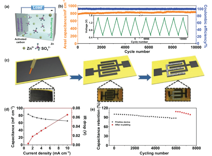
Figure 13. Microhybrid multivalent cation capacitors. (a) Mechanism of Zn-based hybrid MSCs. (b) Cycling stability at a current density of 1.56 mA cm−2. Inset shows the first five and the last five GCD profiles of the Zn-based hybrid MSCs. [198] John Wiley & Sons. © 2018 WILEY-VCH Verlag GmbH & Co. KGaA, Weinheim. (c) Schematic illustration of the preparation process for the HZICs. (d) Areal capacitances and IR drop versus various current densities. (e) Cycling performance of the HZICs at 5 mA cm−2. Reproduced from [200], with permission from The Royal Society of Chemistry.
Download figure:
Standard image High-resolution imageIn the reaction process of Zn-based hybrid capacitors, Zn is repeatedly deposited and stripped during charging and discharging; and the Zn anode is inevitable to be constantly consumed [199]. For the macroscopic device, the consumption of the Zn anode is always neglected because the Zn tends to be excessive under most circumstances. By contrast, regulating the consumption of Zn is a tough challenge in the microscopic device, where the Zn anode is always obtained through electrodeposition in a limited content. Moreover, the irreversible dissolution of Zn2+ ions will result in capacity degradation and poor cycle performance, largely restricting the overall performance of Zn-based hybrid capacitors. To address this difficulty and to achieve high energy output and prolonged cycle life of the microdevices, Sun et al fabricated a capacity recoverable HZIC by laser carving and the electrodeposition method (figure 13(c)) [200]. In a typical process, the polyimide tape and commercial CNT paper served as the substrate and active material for the cathode, respectively. The CNT paper was firstly pasted onto the polyimide tape, and the interdigital microelectrodes were fabricated through a computer-controlled laser cut technology. After that, the Zn anode was deposited and replenished through electrodeposition, whenever necessary, which did no damage to the structure of the designed zinc-based hybrid capacitors. Due to the non-faradaic reaction of the cathode and the faradaic capacitive reaction of the anode, the proposed HZICs showed a low infrared (IR) drop even under a high current density (0.065 V at the current density of 10 mA cm−2) and delivered an excellent areal capacitance of 83.2 mF cm−2 at 1 mA cm−2 (figure 13(d)). In addition, the prepared HZICs still maintained a capacitance of about 87.4% (60.9 mF cm−2) after 6000 cycles. More surprisingly, a higher areal capacitance of 76 mF cm−2 and the prolonged cycling life were also observed after the Zn was re-plated (figure 13(e)). The proposed prolonged HZICs feature an uncomplicated design and practical operation in miniaturized devices, possessing great potentialities for applications with extremely long service.
7. On-chip integrated microsystems
In addition to the continuing efforts to fabricate miniaturized and appropriate devices using a method that cuts costs and improves electrochemical energy storage performance, considerable attention has also been given to the integration of energy devices with target-oriented functions [201–206]. The on-chip integration of specific functions into MESDs can endow them with more impressive properties, making them suitable and accessible for microsystem applications. An ideal on-chip integrated system based on MESDs should not only possess high electrochemical performance with good durability but also be well endowed with the desired properties for specific purposes. In this field, MESDs integrated with harvesters, screen displays, fuel cells, transmitters, and electrochromic and miscellaneous sensors have been extensively studied so far [24, 207–211].
The combination of miniaturized energy storage systems and miniaturized energy harvest systems has been seen as an effective way to solve the inadequate power generated by energy harvest devices and the power source for energy storage devices. For example, Jiang et al proposed a highly compact, self-powered system by combining a TENG and MXene-based MSCs in a flexible harvest-storage unit [206]. Fan's group successfully demonstrated an integrated, self-powering smart system with embedded solar cells and printed supercapacitors for energy harvest and energy storage and a printed gas sensor for ethanol and acetone detection [212]. More recently, Qiu et al designed an all-in-one energy system consisting of urea-based photocatalytic fuel cells (PFCs) and MSCs to power miniaturized electronic devices (figure 14(a)) [213]. The planar PFCs were composed of a titanium dioxide (TiO2) photoanode and an Ag counter electrode, and it proved to exhibit stable energy output. In the meantime, the proposed all-in-one system successfully used the urea as fuel to purify wasted water, reaching a high power density of 3.04 μW cm−2 under a UV intensity of 30 mW cm−2 in 1 M urea solution. The incessant energy generation from PFCs is schematically displayed in figure 14(b). Under the exposure of the UV light, electron-hole pairs were generated from the TiO2 photoanode. Then the absorbed urea molecules were oxidized after the holes moved to the surface of the TiO2. For continuous output, the electrons that were left would be transferred to the external circuit; and then the energy could be stored by MSCs or directly power electronic devices. Overall, this sustainable and eco-friendly system possesses great promise for self-powered, portable electronics and microsystem applications.

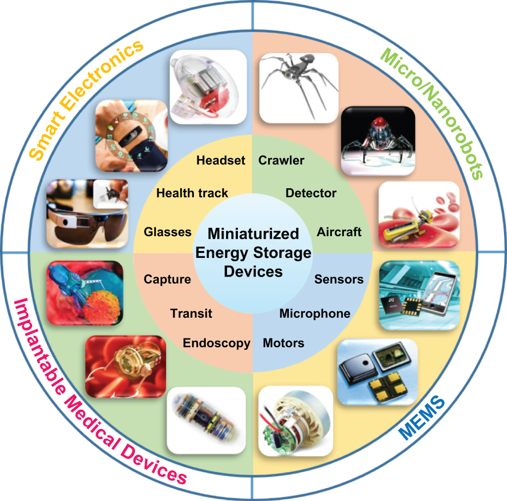
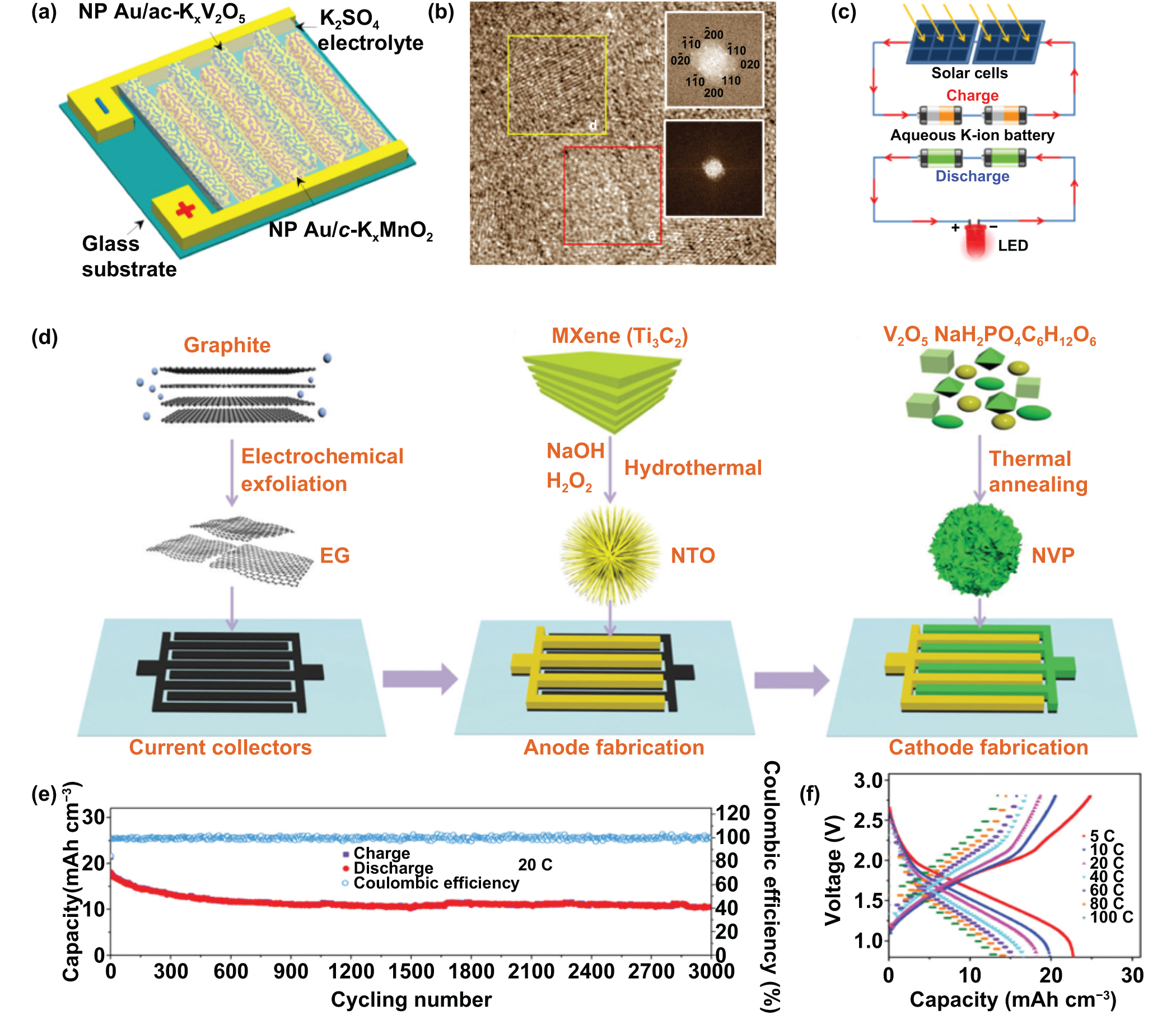
Figure 14. On-chip integrated microsystems. (a) Flexible all-in-one system composed of photocatalytic fuel cells (PFCs) and asymmetric MSCs. (b) Mechanism of energy generation from the PFC in urea solution under UV irradiation. Reproduced with permission from [213]. Copyright (2019), American Chemical Society. (c) Schematic illustration of the light permeability and hazing effect of the microbattery. (d) Digital photographs of the electrolytes with emission in different colors under UV light illumination. Reproduced from [214], with permission from The Royal Society of Chemistry. (e) A photograph and a schematic of the transmitter. Reprinted from [215], Copyright (2018), with permission from Elsevier. (f) Schematic of the tandem MSCs bridging solar cells and a gas sensor to store solar energy and supply energy. [216] John Wiley & Sons. © 2017 WILEY-VCH Verlag GmbH & Co. KGaA, Weinheim.
Download figure:
Standard image High-resolution image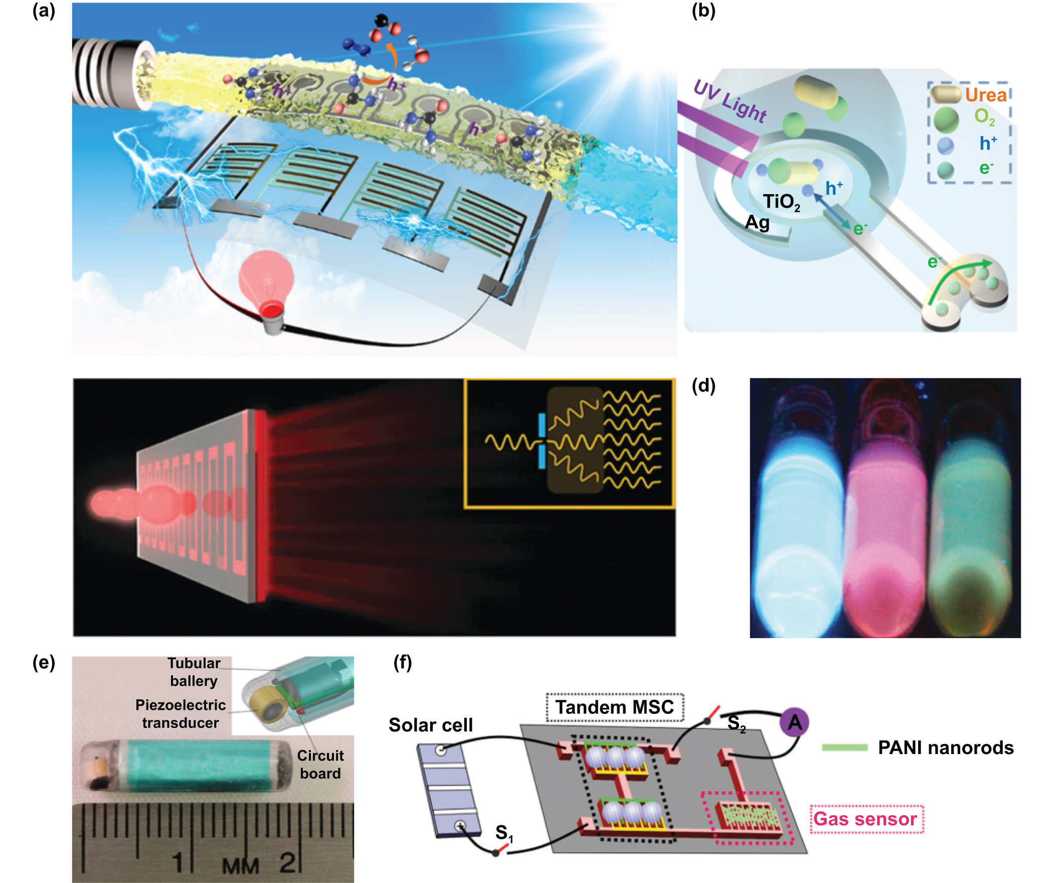
The battery and screen are considered to be the two main components that occupy the largest volume in most electronic devices. Integrating the battery with the screen is believed to greatly decrease the size of electronic devices, which has been a long-term challenge for researchers. Zhi's group was the first to introduce a battery-in-screen design that successfully integrated the microbattery into the screen [214]. The integrated system was based on a microbattery with a unique hydrogel electrolyte, which was embedded with water-soluble, photoluminescent quantum dots. The well-designed microbattery exhibited a high energy density, and displayed stable photoluminescent performance during repeated cycling. The compact array of the microbattery could effectively provide energy for the UV backlight in the screen and could also serve as a color filter for the full color display screen. Figure 14(c) shows the light permeability of the battery-in-screen, where the light can easily permeate the structure and simultaneously be scattered when the microbattery is illuminated by a point light source from the back. Furthermore, figure 14(d) displays the emission of three primary colors (red-green-blue (RGB)) from the photoluminescent electrolytes under UV light illumination. The configuration of battery-in-screen intermixes the two largest volumetric parts, holding enormous potential for significantly decreasing the volume of integrated electronic systems.
Apart from the integrations mentioned above, MESD systems integrated with chemical-biomedical-physical sensors and executors have also aroused extensive interest in recent years. Xiao's group reported the fundamental issues involved in designing structural MBs and then demonstrated a functional acoustic transmitter driven by a tubular microbattery [215]. To evaluate the practical performance, a tubular microbattery, with a diameter of 4.8 mm, was put into an acoustic underwater transmitter, where the electronic elements were all tucked inside the tube (figure 14(e)). The transmitter system consists of three parts: the signal transmission, controlling unit, and energy source. In addition to the tubular microbattery, there was also a piezoelectric transducer for signal transmission and a circuit board for the control circuit. The service life was further tested at a ping rate of 3 s underwater, and an authentic signal through the integrated transmitter system could be received clearly through the underwater hydrophone.
When it comes to compatible substrates for MESDs, paper-based substrates have been regarded as the ideal flexible substrates due to their low cost and disposability. In addition, paper-based substrates have a rough, porous surface that is beneficial for enhancing the interface adhesion with electronic devices. Guo et al reported a flexible in-plane MSC integrated with sensors in [216]. To meet practical demands with different conditions, two fabricated MSCs, connected in series, were obtained to improve the output voltage. Moreover, the effective bridging of tandem MSCs with solar cells and sensors (figure 14(f)) favorably realized the integration of energy generation, energy storage, and application, demonstrating the feasible potential of a completely wireless, flexible sensor system on a paper substrate. Moreover, the ZnO-based UV sensor and the PANI-based gas sensor were successfully constructed in this integrated system, developing a novel, paper-based strategy for future portable and wearable electronics.
8. Conclusions and prospects
MESDs are expected to play an indispensable role as a practicable energy supply for miniaturized electronic devices, with ever-increasing development over the last decade. The recent advances in MESDs were systematically summarized in this review. We briefly introduced the concept of MESDs and elucidated their superiorities, such as their ultracompact size with compatible power, highly customizable electrochemical performance, and capability of being easily integrated with specific microsystems on a chip or flexible substrate, which could serve as a complement to conventional energy storage systems. Meanwhile, the general definition of miniaturized devices was provided to distinguish them from conventional energy storage devices. The configuration design of MESDs (2D stacked, 2D planar interdigital, 2D arbitrary-shaped, 3D planar, and wire-shaped) and electrode microfabrication strategies, such as printing, scribing, and masking techniques, were also briefly generalized in this paper. In addition, MBs, MSCs, and MHMICs, major elements of MESDs, were further subdivided and summarized in turn. On-chip integrated MESD microsystems with specific functions were separately proposed to highlight the unique advantages of MESDs under specific application scenarios.
From the recent advances and achievements of MESDs, it is worth noting that the challenges are not only to enhance the electrochemical property, such as high energy and high power density, in a limited footprint with a durable lifetime but also to integrate with multifunctional properties, matching up with multiple demands of microelectronic devices and microsystems. In order to better promote the development of MESDs, future research on MESDs should pay more attention to the following aspects.
First, the configuration design of MESDs will take more diverse and sophisticated forms for special applications, even for some extremely complex conditions. Research on the intricate connections among the structure design, electrolyte selection, ion transport, and electrochemical property is essential for the improvement of advanced MESDs. For instance, constructing 3D micro/nanostructures with high mass loading of active materials, large specific surface area, and superior electrical conductivity has gradually been regarded as a trendy method of enhancing the areal or volumetric energy density. In addition, optimization of specific parameters of the microelectrodes, such as the effective area among the entire device, a proper interspace, and length and width for the single electrode, is highly needed. An urgent need for MESDs with arbitrary shapes has been growing, while the related research is still scant due to the limited flexible manufacturing technology. It should be noted that the various configurations of MESDs should rely on the development of advanced electrode materials, electrolytes, storage mechanisms, and electrode manufacturing techniques.
Second, developing easy-to-operate, low-cost, time-saving, highly safe, environmentally friendly, and scalable microelectrode fabrication technologies is urgently needed to realize the widespread application of MESDs and on-chip integrated microsystems. Up to now, various advanced microelectrode fabrication strategies have been used for microdevices, including 3D printing, transfer printing, mask-assisted filtration, photolithography, electrodeposition, laser scribing, and so on. In an ideal situation, the microelectrodes should be directly fabricated on the substrate and easily integrated, rather than being transferred from one substrate to another. Accordingly, printing technologies, especially 3D printing, has been regarded as one of the most prospective technologies for the mass production of MESDs. First, the thickness of the microelectrodes can be accurately regulated in a wide range, from tens of micro/nanometers to hundreds of millimeters. In addition, the fabricated microelectrodes are expected to be directly printed on the target substrate via 3D printing, which further promotes the on-chip integration and functionalization of MESDs. Moreover, the asymmetric microelectrodes can be individually printed to improve the electrochemical performance through different printing materials. Especially, 3D printing is capable of fabricating MESDs with miscellaneous shapes and structures, contributing to a bright future for flexible manufacturing. More importantly, the electrolyte and in situ encapsulation of microdevices can also be obtained through 3D printing, which shows superior convenience to other microfabrication techniques and is another key factor for practical application. Given these reasons, it is believed that 3D printing will promote the development of next-generation MESDs and facilitate the integration of microsystem applications.
Third, high-performance and multifunctional active materials on microelectrodes are highly needed to further meet the ever-growing power demand and special mechanical requirements, such as bendability and stretchability. Considering the potential advantages, nanostructured porous materials with a highly conductive network are predicted to promote fast electron transfer and ion diffusion, which makes them become promising candidates for MESDs with high areal and volumetric performance. Furthermore, quasi in situ or in situ characterization technologies have been proven to serve as quite useful means for studying the mechanism of energy storage devices; but relevant research in MESDs remains insufficient. The development of characterization methods (e.g. in situ Raman spectroscopy [217], in situ x-ray diffraction pattern [218], in situ scanning/transmission electron microscopy and SEM [219], and in situ nuclear magnetic resonance spectroscopy [220]), is also vital to understand the reaction mechanism and micro/nanostructure evolution of active materials during the charge/discharge process for the fundamental research of new advanced materials and miniaturized electrochemical devices.
Four, advanced electrolytes should be taken into serious consideration to match the high-performance active materials for next-generation MESDs. Liquid electrolytes, including aqueous electrolytes, organic electrolytes, and ionic liquid-based electrolytes, possess high power and superior rate capability due to their naturally high ionic conductivity. However, addressing the problem of electrolyte leakage and the protective encapsulation technology for stable operation is still urgently needed. Consequently, quasi-solid-state/solid-state electrolytes, such as aqueous gel-based electrolytes, inorganic/organic solid-state electrolytes, and ionogel-based electrolytes, are expected to be excellent selections for practical application of MESDs. They cannot only deliver relatively low leakage current, long cycle life, and outstanding electrochemical properties but also come with sufficient mechanical strength and thermal stability. What is more, the redox-based electrolytes may be another effective choice for MESDs since they can provide extra charge storage in the reaction process and thus boost the capacity, which also deserves further in-depth research in the future.
Finally, achieving self-powering, multifunctional on-chip integrated microsystems consisting of energy harvesting, energy storage, and energy consumption devices is an undoubted future trend for both MESDs and MEMS applications. Various miniaturized energy harvest devices, such as TENGs and PENGs for mechanical motion/vibration energy, photovoltaic devices for solar energy, and thermoelectrics for thermal energy, can be coupled with MESDs to effectively convert renewable energy sources into electricity and conserve energy. Furthermore, the integrated self-powered electronic devices can simultaneously be utilized to power microelectronic devices (e.g. miniaturized chemical-biomedical-physical sensors and screen displays), realizing a fully integrated microsystem. It should be noted here that the overall energy efficiency from the initial harvester to the final electronics should also be taken into serious consideration, which could be a vital factor for improving the compatibility and practicability of the whole system.
Considering the promising prospects, researchers still need to explore more possibilities to perfect the development and application of MESDs. Engineers need to seek to apply them to practical uses, such as wearable devices, implanted devices, and micro/nano systems. While there is still a long way toward making it a reality, the potential of MESDs is truly tantalizing.
Acknowledgments
We gratefully acknowledge the financial support from the National Natural Science Foundation of China (Grant Nos. 51702095, 51722503, 51975204), Natural Science Foundation of Hunan Province, China (Grant No. 2018JJ3041), the Fundamental Research Funds for the Central Universities (531118010016), and Science and Technology Bureau Foundation of Changsha City (kh1904005).
Conflicts of interest
The author declares no conflicts of interest.