

Abstract
Earth-abundant and environmentally benign antimony selenide (Sb2Se3) has emerged as a promising light-harvesting absorber for thin-film photovoltaic (PV) devices due to its high absorption coefficient, nearly ideal bandgap for PV applications, excellent long-term stability, and intrinsically benign boundaries if properly aligned on the substrate. The record power conversion efficiency of Sb2Se3 solar cells has currently reached 9.2%, however, it is far lower than the champion efficiencies of other chalcogenide thin-film solar cells such as CdTe (22.1%) and Cu(In,Ga)Se2 (23.35%). The inferior device performance of Sb2Se3 thin-film solar cells mainly results from a large open-circuit voltage deficit, which is strongly related to the interface recombination loss. Accordingly, constructing proper band alignments between Sb2Se3 and neighboring charge extraction layers through interface engineering to reduce carrier recombination losses is one of the key strategies to achieving high-efficiency Sb2Se3 solar cells. In this review, the fundamental properties of Sb2Se3 thin films, and the recent progress made in Sb2Se3 solar cells are outlined, with a special emphasis on the optimization of energy band alignments through the applications of electron-transporting layers and hole-transporting layers. Furthermore, the potential research directions to overcome the bottlenecks of Sb2Se3 thin-film solar cell performance are also presented.
Export citation and abstract BibTeX RIS

Original content from this work may be used under the terms of the Creative Commons Attribution 4.0 license. Any further distribution of this work must maintain attribution to the author(s) and the title of the work, journal citation and DOI.
1. Introduction
Conventional thin-film photovoltaic (PV) devices, such as cadmium telluride (CdTe), copper indium gallium selenide (Cu(In,Ga)Se2) solar cells with demonstrated record efficiencies of 22.1% [1] and 23.35% [2], respectively, exhibited the impressive achievements in the field of PVs. However, the toxicity of Cd and the scarcity of In and Ga would ultimately limit the terawatt-scale (TW)-scale deployment of these technologies. In this perspective, it is imperative to find an appropriate replacement that consists of non-toxic and abundant elements. Recently, environmentally benign and earth-abundant antimony selenide (Sb2Se3) has emerged as a promising light-harvesting absorber owing to its attractive properties for PV applications, such as bandgap, high absorption coefficient, decent carrier mobility, simple binary phase composition, excellent long-term stability, and intrinsically benign grain boundaries, if properly oriented [3–5]. Remarkable achievements have been made in the Sb2Se3 solar cells during the last decade (figure 1)—Sb2Se3 solar cells have exhibited a considerable increase in the power conversion efficiency (PCE) from 2.26% [6] to 9.2% [7] over a five-year period, thus garnering extensive attention in recent years.

Figure 1. Major progress in antimony selenide solar cells: 2.26% [6], 3.21% [11], 3.7% [12], 5.6% [13], 6.5% [14], 7.6% [15], and 9.2% [7].
Download figure:
Standard image High-resolution imageIn spite of such progress, the current champion device efficiency of Sb2Se3 solar cells is still far below the theoretical prediction of ∼32% [8], implying that there remains significant room for device performance improvement. This striking difference between the state-of-the-art cell efficiency and the theoretical limit of the Sb2Se3 solar cell is primarily attributed to its large open-circuit voltage (Voc) deficit, which is generally defined as Eg/q−Voc [4, 9]. It is reported that the Voc loss is largely subjected to Shockley-Read-Hall (SRH) recombination (also called trap-assisted recombination) and interface recombination induced by improper band alignments between the Sb2Se3 light absorber and its neighboring layers [10]. Chen and Tang pointed out that the interface recombination outweighs SRH recombination, although both recombination mechanisms contribute to the performance loss of antimony chalcogenide (Sb2Se3, Sb2S3 and Sb2(S,Se)3) solar cells [9]. For this reason, the optimization of band alignments (also called energy-level alignments) must be carefully conducted to suppress the interface recombination, aiming to reduce the Voc-deficit of Sb2Se3 solar cells.
There have been only several review articles on Sb2Se3 solar cells in the literature and none of these articles presents a thorough discussion of band alignments. In this review, we overview the recent advances in Sb2Se3 thin-film solar cells with a special emphasis on interface engineering through band alignment optimization, providing new insights into strategies for PV performance enhancements. Following the introduction part (section 1), we discuss the material properties of Sb2Se3 (section 2). Then, we briefly present the typical device architectures of Sb2Se3 solar cells (section 3), after which, we discuss the band alignment optimization strategies, involving various electron-transporting layers (ETL) and hole-transporting layers (HTL) (section 4). Lastly, we share our perspectives on current challenges as well as potential development directions in Sb2Se3 thin-film solar cells.
2. Basic properties of Sb2Se3
Sb2Se3 belongs to a family of binary V2–VI3 compounds whose group members include Sb2Se3, Sb2S3, Sb2Te3, Bi2Se3, Bi2S3, Bi2Te3. Among these V2–VI3 compound materials, only a few of them have been reported for PV applications, despite their similar crystal structures. As previously stated, Sb2Se3 has particularly received tremendous interest within the PV community over the last decade because of its excellent optoelectronic properties. Here, we briefly summarize the main physical parameters of Sb2Se3 as listed in table 1 and introduce other unique physical properties more in detail.
Table 1. Summary of main physical parameters of Sb2Se3.
| Parameter | Value | Reference |
|---|---|---|
| Crystal lattice constants | ||
a ( ) ) | 11.6330 | [6] |
b ( ) ) | 11.7800 | |
c ( ) ) | 3.9850 | |
| Space group | Pbnm 62 | [16, 17] |
| Density (g cm−3) | 5.84 | [18] |
| Melting point (K) | 885 | [18] |
| Absorption coefficient (cm−1) |
 105 105
| [19] |
| Relative dielectric constant | 14.3–19.8 | [3, 18] |
Conductivity ( cm)−1 cm)−1
| 10−5–10−7 | [20–22] |
| Mobility (cm2 V−1 S−1) | ||
Hole mobility ( ) ) | 15 | [18] |
Electron mobility ( ) ) | 42 | |
| Minority-carrier lifetime (ns) | 67  7 7 | [20] |
Diffusion length ( m) m) | 1.7  0.2 0.2 | [20] |
| Exciton binding energy (eV) | 1.28 | [23] |
| Bandgap (eV) | ||
| Indirect bandgap | 1.03 | [19, 24] |
| Direct bandgap | 1.17 |
2.1. Crystal structure
Sb2Se3 is a binary compound existing in the form of stibnite and owns an orthorhombic structure. As depicted in figure 2, the atomic arrangement shows that Sb2Se3 contains the Se–Sb–Se chains along the c-axis, with relatively low symmetry. In quasi-one-dimensional (Q1D) Sb2Se3, the crystal structure consists of 1D [Sb4Se6]n building blocks where the atoms are covalently bonded within the ribbons, while the van der Waals force exists between the ribbons. Recombination loss often occurs at the grain boundaries (GBs) in a 3D crystal structure, in which the dangling bonds act as recombination centers, resulting in the degradation of device performance, while GBs between 1D ribbons in Sb2Se3 are free of dangling bonds when the ribbons are suitably oriented [13]. For instance, parallel-stacked [Sb4Se6]n ribbons along the [001] direction are free from dangling bonds, thereby suppressing the carrier recombination at the GBs and minimizing recombination losses.

Figure 2. Crystal structure of Sb2Se3: (a) orthorhombic structure of Sb2Se3 and [Sb4Se6]n ribbons stacked along [001] direction with benign grain boundaries (GBs), and (b) atomic configuration of (010) and (100) surfaces in Sb2Se3. Reproduced from [13], with permission from Springer Nature.
Download figure:
Standard image High-resolution imageDensity functional theory revealed that the electron density is concentrated within the [Sb4Se6]n ribbons and thus the GBs are electrically benign [13, 25]. Furthermore, it is calculated that the surfaces orthogonal to the (001) plane, such as (120), (110), (100), and (010), are the most prevalent planes in Sb2Se3, thanks to the lower surface energies as well as the absence of covalent bond breakage [5]. Hence, as long as the [Sb4Se6]n ribbons are oriented along the direction of vertical charge transport in PV devices, the recombination at the GBs will be minimized. This structural characteristic of Sb2Se3 makes it particularly favorable for PV applications as recombination losses at GBs are one of the major limitations for high-performance thin-film solar cells.
2.2. Defect properties
As previously mentioned, Sb2Se3 owns a unique Q1D crystal structure compared to most well-known inorganic PV absorbers with a 3D crystal structure such as CdTe, Cu(In,Ga)Se2 (CIGS), and Cu2ZnSnS2 (CZTS). For those traditional light-absorbing materials with 3D structures, the breakage of covalent bonds unavoidably introduces intrinsic defects and thus requires passivation strategies to remedy this problem. Therefore, it is of great significance to understand the fundamentals of defects properties in Sb2Se3 and thus further control the defects to enhance device performance.
The intrinsic defects properties of Sb2Se3 were expected to be simple on account of a binary nature. Through a combined experimental and theoretical investigation, Liu and his co-authors [26] revealed that there are five intrinsic point defects in Sb2Se3 (figures 3(a) and (b)), including two substitutions (SbSe, SeSb), two vacancies (VSe, VSb) and one interstitial (Sei). They further pointed out that the deep donor defects, SbSe and VSe would dominate in Sb2Se3 under Se-poor conditions, whereas the more benign defects, the shallow acceptor defect SeSb and the inert defect Sei, would prevail in a Se-rich environment. However, further investigations have exhibited that Sb2Se3 has much more unexpectedly complicated and unconventional intrinsic defect chemistry compared to conventional semiconductors. Huang et al [27] reported that, based on the property of point defects in Sb2Se3, all these point defects could be classified into three types: five antisites (SbSe1, SbSe2, SbSe3, SeSb1, SeSb2), five vacancies (VSb1, VSb2, VSe1, VSe2, VSe3), and non-equivalent interstitials (Sbi, Sei) (figures 3(c) and (d)). They identified SbSe1, SbSe2, and SbSe3 defects as donor defects, and SeSb1, and SeSb2 as acceptor defects. However, Savory and Scanlon [28] have proposed for the first time that SbSe1 SbSe2, SbSe3, SeSb1, and SeSb2 are amphoteric defects. In other words, these defects could be both hole and electron traps, namely, donor-type and acceptor-type defects, respectively. More specifically, SbSe1, SbSe2, and SbSe3, which are dominant defects under Se-poor conditions, are amphoteric, while under a Se-rich environment, both SeSb1 and SeSb2 antisites are amphoteric defects. Despite the different results on the nature of point defects in Sb2Se3, the previous studies have agreed that an intrinsic defect concentration is higher under Se-poor conditions than under Se-rich conditions. Hence, a Se-rich condition is more desired in the preparation of Sb2Se3 in order to achieve a longer minority carrier lifetime, better p-type conductivity, and higher cell performance.

Figure 3. Defect properties of Sb2Se3: (a), (c) energy level of intrinsic defects at different atomic sites in the Sb2Se3 bandgap. [26] John Wiley & Sons. Copyright © 2017 John Wiley & Sons, Ltd. (b), (d) Under the Se-rich and Se-poor (Sb-rich) conditions in Sb2Se3, the formation energies and equilibrium concentrations of different defects are calculated as functions of the Fermi level. Reprinted with permission from [27]. Copyright (2019) American Chemical Society.
Download figure:
Standard image High-resolution image2.3. Electrical and optical properties
The Q1D ribbon-like structure of Sb2Se3 naturally leads to anisotropy in charge-transport property and thus in electrical conductivity. Sb2Se3 is generally weakly p-type due to its relatively low intrinsic charge carrier concentration ( 1013 cm−3) [20]. Some groups have reported that Sb2Se3 can also exhibit n-type conductivity when extrinsic doping is performed [29, 30].
It is well-known that the minority carrier diffusion length is one of the key factors to determine the PV performance of solar cells. A long minority carrier diffusion length will promote the electron collection, and thereby contribute to higher light-harvesting efficiency. Additionally, the photo-generated carrier lifetime also plays a critical role in determining PV performance. Transient absorption decay spectroscopy results revealed that the carrier recombination lifetime of around 100 ns [26]. The electron mobility of Sb2Se3 is reported to be about 15 cm2V−1S−1, and the hole mobility is about 42 cm2V−1S−1 (summarized in table 1), which is comparable to those of CdTe. Another key material property of good light absorbers is the dielectric constant. A larger dielectric constant usually gives rise to a lower exciton binding energy which means an easy separation of electron–hole pairs upon photoexcitation. The dielectric constant of Sb2Se3 has been reported to be 14.3–19.8, which is larger than that of CdTe (7.1) and CIGS (13.6) [3].
It is known that the optical properties of Sb2Se3 strongly depend on its chemical composition (i.e. Sb to Se ratio). The bandgap of polycrystalline Sb2Se3 with the stoichiometric composition has been reported to be in the range of 1.0–1.3 eV [19, 31–35]. With the in-depth study of Sb2Se3, further understanding of the physical properties of Sb2Se3 and more accurate bandgap values have been obtained. Chen et al [19] have summarized the overall optical properties of Sb2Se3, showing that polycrystalline Sb2Se3 has a direct bandgap of 1.17 eV and an indirect bandgap of 1.03 eV at room temperature, which was confirmed by the temperature-dependent transmission spectrum, as presented in figure 4(a). The direct bandgap of 1.17 eV is in the optimal range considering Shockley–Queisser (S–Q) limit.

Figure 4. Optical properties of Sb2Se3: (a) Temperature-dependent bandgap of Sb2Se3, and (b) the incident light intensity decay versus wavelength and thickness. The dashed line shows the relation between the absorption coefficient and wavelength. Reprinted from [19], with the permission of AIP Publishing.
Download figure:
Standard image High-resolution imageIn addition to a proper bandgap, a high absorption coefficient ( 105 cm−1) in the visible and ultraviolet spectrum of Sb2Se3 allow sufficient absorption of the solar spectrum within a relatively thin absorber. The high absorption coefficient is ascribed to the electronic structure of Sb2Se3, where the flat electronic bands of Sb2Se3 are expected to gain enhanced light absorption owing to the high density of states existing in the conduction band minimum (CBM) and the valence band maximum [36]. Figure 4(b) shows the wavelength-dependent decay of incident light. These results demonstrated that the photons with wavelengths larger than 800 nm can be absorbed completely by a 400 nm-thick Sb2Se3 film, which is thinner than other conventional light absorbers such as CIGS and CdTe.
3. Device configurations
Sb2Se3 solar cells with various device configurations have been demonstrated with progress in recent years. The device configurations of Sb2Se3 solar cells are classified into two main types—mesoporous sensitized and planar architecture. The planar-type structure can be further divided into two configurations, namely, substrate and superstrate structure. The schematic illustrations of the device structures are shown in figure 5.

Figure 5. Schematic illustrations of typical device architectures of Sb2Se3 solar cells: (a) mesoporous sensitized structure, (b) substrate planar structure, and (c) superstrate planar structure.
Download figure:
Standard image High-resolution image3.1. Mesoporous sensitized architecture
In a typical mesoporous sensitized structure (figure 5(a)), a wide bandgap metallic oxide is an indispensable component, serving as an electron transporting layer. Among the various metallic oxides, TiO2 is the most promising candidate because of its advantages for sensitized photo-electrochemistry, that is, abundance, low cost, non-toxicity, and biocompatibility. A compact TiO2 layer is usually deposited on an indium tin oxide (ITO) or fluorine-doped tin oxide (FTO) substrate first, and then, a thick mesoporous TiO2 scaffold layer is spin-coated onto the compact TiO2 layer. The Sb2Se3 absorber layer is then fabricated on the scaffold TiO2 layer, and an HTL is subsequently covered on the absorber layer. In the end, a metal electrode such as Au is deposited on the HTL by thermal evaporation. Electron extraction benefits greatly from the scaffold structure consisting of mesoporous TiO2, which is known to compensate for the insufficient electron transport due to the short minority carrier diffusion length induced in the Sb2Se3 absorber.
It is well accepted that the mesoporous sensitized-type Sb2Se3 solar cells have evolved from solid-state dye-sensitized solar cells (DSSCs) [37, 38]. The efficient charge separation between Sb2Se3 nanoparticles and mesoporous TiO2 layer in a sensitized solar cell was demonstrated by Guijarro et al [39], although there was no cell performance reported from a complete device in their research. Despite the active research on sensitized Sb2Se3 solar cells, further developments have been limited to cell efficiencies below 3% with the mesoporous structure [40, 41], which is attributed to charge carrier recombination at the mesoporous TiO2/Sb2Se3 interface.
3.2. Planar architecture
The mesoporous Sb2Se3 devices tend to have a relatively low Voc, leading to lower PV performance, thereby attention has been given to a simpler device structure—the planar-type structure, which has achieved better device performance than the mesoporous-type structure. The planar-structured devices are further divided into two types: substrate-, and superstrate-structure.
The substrate structure of Sb2Se3 solar cells originates from the conventional device configuration of CIGS solar cells [42, 43]. As illustrated in figure 5(b), the substrate structure generally consists of a Mo-coated glass substrate, a Sb2Se3 absorber layer, an ETL (e.g. CdS), a transparent conductive oxide (TCO) transparent electrode (e.g. i-ZnO, and ZnO:B, etc), and a grid electrode (e.g. Ag). The substrate structure allows the absorber/buffer heterojunction to be optimized separately and there is no strict requirement on the substrate materials as long as they have no detrimental effects on cell performance [44]. Additionally, the possible application to tandem solar cells makes the substrate architecture more attractive [45]. Despite the versatility offered by the substrate configuration, there is a limited number of publications on substrate-type Sb2Se3 solar cells [42, 46–48].
The superstrate device configuration mainly consists of TCO substrate/ETL/Sb2Se3 absorber layer/HTL/metal electrode (figure 5(c)). Recently, p–i–n and n–i–p device structures in superstrate configurations have been reported by numerous research, where p, i, and n are acceptor-, intrinsic-, and donor-type semiconductor, respectively. In these device configurations, the quasi-intrinsic absorber is generally accompanied by p-type HTLs and n-type ETLs to improve carrier extraction efficiency. Besides, the construction of n–i–p device configuration is a feasible way to reduce the carrier recombination at the back surface through the formation of a back surface electric field [49]. In contrast to the substrate device configuration, the requirement that the substrate material must be transparent in the visible region still limits the practical application of the superstrate device configuration to some extent. Thus far, the champion cell efficiencies of substrate-type and superstrate-type Sb2Se3 solar cells are 9.2% [7] and 7.6% [15], respectively. However, several research groups recently have claimed that an n–i–p device structure (belonging to a superstrate structure) is a more promising option for developing high-efficiency Sb2Se3 solar cells [14, 49, 50]. Therefore, there is still no consensus on the optimal device configuration of Sb2Se3 solar cells. It is necessary to make full use of the advantages of different device configurations considering their pros and cons.
4. Energy band alignment optimization
Energy band alignment of a semiconductor junction is generally used to describe how the conduction band (CB) and valence band (VB) of two materials line up to form a heterojunction, and it critically influences the behavior of the semiconductor junction. Upon forming a heterojunction with two semiconductors with different bandgaps and different work functions, discontinuities of CBs and VBs at the interface are often referred to the conduction band offset (CBO) and valence band offset (VBO), respectively. The formation of the band offsets is crucial to the performance of heterojunction solar cells. Generally, there are two types of band offsets at the heterojunction: type I ('spike-like') and type II ('cliff-like'), as displayed in figure 6 [51]. A 'spike-like' band offset (figure 6(a)) is formed when the CBM of an absorber layer lies below the CBM of a buffer or a window layer, while a 'cliff-like' band offset (figure 6(b)) describes the opposite situation. The 'spike-like' (positive CBO) energy level alignment is found to be more favorable for the suppression of interface recombination due to the formation of a potential barrier at the heterointerface. Nonetheless, a too positive CBO will give rise to a too high potential barrier for the charge transport, leading to a lower short-current density (Jsc) and thus a lower cell efficiency. On the contrary, the 'cliff-like' energy level alignment (negative CBO) lowers the potential bandgap and consequently facilitates the trap-assisted recombination of charge carriers at the heterojunction interface. The 'cliff-like' offset also limits the built-in voltage of the heterojunction, resulting in a lower open-circuit voltage (Voc). Therefore, it is crucial to construct an optimal energy band alignment, a slightly 'spike-like' configuration. As ETLs and HTLs play a vital role in modifying the energy band alignments in Sb2Se3 solar cells, we hereby put a special emphasis on the research on ETLs and HTLs (figure 7) and summarized Sb2Se3 devices with various ETLs and HTLs reported in the literature (table 2).

Figure 6. Schematic illustrations of band alignment with different types of conduction band offset (CBO): (a) a 'spike-like' (positive) CBO, and (b) a 'cliff-like' (negative) CBO. Reprinted with permission from [51]. Copyright (2020) American Chemical Society. <https://pubs.acs.org/doi/10.1021/acsaem.0c01477> Further permissions related to the material excerpted should be directed to the ACS.
Download figure:
Standard image High-resolution image
Figure 7. Energy-level alignment of various ETLs and HTLs together with antimony selenide absorber layer.
Download figure:
Standard image High-resolution imageTable 2. Summary of Sb2Se3 devices with various ETLs and HTLs.
| Device structure | Type of configuration | ETL | HTL | PCE (%) | Reference |
|---|---|---|---|---|---|
| Mo/Sb2Se3/Cdx Zn1−x S/i-ZnO/AZO | Substrate | Cdx Zn1−x S | / | 6.71 | [52] |
| FTO/SnO2/CdS:O/Sb2Se3/Spiro-OMeTAD/Au | Superstrate | CdS:O | Spiro-OMeTAD | 6.29 | [53] |
| FTO/ZnO/Sb2Se3/Au | Superstrate | ZnO | / | 4.08 | [54] |
| FTO/ZnO/Sb2Se3/Au | Superstrate | ZnO | / | 5.93 | [55] |
| FTO/TiO2/Sb2Se3/Au | Superstrate | TiO2 | / | 5.48 | [56] |
| ITO/TiO2/Sb2Se3/Au | Superstrate | TiO2 | / | 5.33 | [57] |
| FTO/SnO2/Sb2Se3/Au | Superstrate | SnO2 | / | 3.05 | [58] |
| FTO/SnO2/Sb2Se3/P3HT/Carbon | Superstrate | SnO2 | P3HT | 4.76 | [59] |
| FTO/TiO2/CdS/Sb2Se3/Spiro-OMeTAD/Au | Superstrate | TiO2/CdS | Spiro-OMeTAD | 3.90 | [60] |
| FTO/CdS/SnO2/Sb2Se3/Au | Superstrate | CdS/SnO2 | / | 5.27 | [61] |
| FTO/CdS/CeO2/Sb2Se3/Au | Superstrate | CdS/CeO2 | / | 5.14 | [62] |
| FTO/ZnO/ZnMgO/Sb2Se3/Au | Superstrate | ZnO/ZnMO | / | 4.45 | [63] |
| ITO/SnO2/TiO2/Sb2Se3/Au | Superstrate | SnO2/TiO2 | / | 5.82 | [64] |
| FTO/CdS/Sb2Se3/CZ-TA/Au | Superstrate | CdS | CZ-TA | 6.84 | [49] |
| FTO/TiO2/Sb2Se3/P3HT/Au | Superstrate | TiO2 | P3HT | 4.30 | [65] |
| ITO/CdS/Sb2Se3/Poly-TPD/Au | Superstrate | CdS | Poly-TPD | 7.00 | [66] |
| ITO/CdS/Sb2Se3/ PbS colloidal quantum dots (CQDs)/Au | Superstrate | CdS | PbS CQDs | 6.50 | [14] |
| ITO/CdS/Sb2Se3/CuSCN/Au | Superstrate | CdS | CuSCN | 7.50 | [67] |
| FTO/CdS/Sb2Se3/NiOx /Au | Superstrate | CdS | NiOx | 7.29 | [68] |
| FTO/CdS/Sb2Se3/WO3−x /Au | Superstrate | CdS | WO3−x | 7.10 | [69] |
| FTO/SnO2/CdS/Sb2Se3/t-Se/Au | Superstrate | SnO2/CdS | t-Se | 7.45 | [50] |
| FTO/CdS/Sb2Se3/VOx /Au | Superstrate | CdS | VOx | 6.33 | [70] |
4.1. ETL
An n-type ETL that forms a heterojunction with a Sb2Se3 absorber plays a key role in determining the performance of Sb2Se3 solar cells. A basic requirement that an ideal ETL should meet, apart from high electrical conductivity and decent carrier mobility, is a proper energy band alignment with minimum CBO [71]. The careful selection of a suitable ETL and modifications to control the absorber layer/ETL heterointerface can make contributions to efficient electron extraction and suppression of the interface recombination. Moreover, in superstrate-type Sb2Se3 solar cells, especially, an ETL also influences crystallographic orientation and surface morphology of the Sb2Se3 absorber layer grown on the ETL, which has been known to affect the properties of Sb2Se3 films. The commonly used single-layer ETLs (including CdS, ZnO, TiO2, SnO2) as well as modified double layers ETLs in Sb2Se3 solar cells are discussed in this section.
4.1.1. Single-layer ETL
CdS, a widely used and well-investigated ETL for CdTe, CIGS, and CZTS solar cells, has been a popular choice for Sb2Se3 solar cells owing to its easy fabrication via facile chemical-bath deposition method and acceptable CB alignment with respect to the Sb2Se3 absorber. Lin et al [72] analyzed the CBO at the CdS/Sb2Se3 interface by numeral simulations, indicating the formation of a 'cliff-like' band alignment (figure 8(a)). Zn-doping was applied to enlarge the low bandgap of undoped CdS (∼2.43 eV), transforming the band alignment type from 'cliff-like' to 'spike-like' (figure 8(b)), which helps to suppress the interface recombination [52]. The transition of band alignment type was also reported by other studies, in which the oxygenated cadmium sulfide (CdS:O) tuned the bandgap of the ETL as well as modified the band alignment (figure 8(c)) [53]. Some groups claimed that the CdS/Sb2Se3 heterointerface is a 'spike-like' band alignment (figure 8(d)) [73]. Dong et al suggested that the contradictory results ('cliff-like' vs 'spike-like' at the CdS/Sb2Se3 interface) could be ascribed to the difficulty in accurately determining the band bending near the surface of an absorber layer, and the dependence of the interfacial electronic structure on fabrication methods [10]. Nonetheless, most of the recent state-of-the-art Sb2Se3 solar cells are based on the CdS/Sb2Se3 heterojunction. However, a parasitic absorption of CdS layer and the toxicity of Cd are continuing concerns. Therefore, Cd-free ETLs with a wider bandgap, such as ZnO, TiO2, and SnO2, have been explored as an alternative to CdS.

Figure 8. (a) Energy level alignment of CdS/Sb2Se3 interface via numeral simulation. Reprinted from [72], Copyright (2018), with permission from Elsevier. (b) Schematics of the energy band alignment between the different Zn-doped CdS buffers and Sb2Se3 absorber. Reprinted with permission from [52]. Copyright (2018) American Chemical Society. (c) The band diagram at Sb2Se3/CdS interface and Sb2Se3/CdS:O. Reprinted from [53], Copyright (2019), with permission from Elsevier. (d) Diagram of energy band alignment at the interface between CdS and Sb2Se3. Reprinted from [73], with the permission of AIP Publishing.
Download figure:
Standard image High-resolution imageZnO is also an attractive semiconductor material employed as ETL in Sb2Se3-based solar cells thanks to its high electron mobility and low crystallization temperature [74]. It has been reported that ZnO forms an acceptable 'cliff-like' band alignment with Sb2Se3, as depicted in figure 9(a) [73]. Wen et al fabricated superstrate-type ZnO/Sb2Se3 solar cells and found that not only the defects in ZnO but also the crystalline orientation of ZnO buffer layer has crucial effects on device performance improvement. They also observed that the annealing atmosphere has a great influence on the electrical and optical properties of ZnO films and consequently on the device performance of Sb2Se3 solar cells. The vacuum annealing process increases the concentration of oxygen vacancies of ZnO films, whereas ambient air annealing reduces the oxygen vacancies, as shown from photoluminescence analysis (figure 9(b)) [54]. Another study [55] shows that the preferential orientation of Sb2Se3 absorber changes with the orientation of ZnO ETL—Sb2Se3 films deposited on a randomly oriented ZnO (r-ZnO) usually exhibits [221] orientation while [120]-oriented Sb2Se3 always dominates on top of [001]-oriented ZnO (o-ZnO) (figure 9(c)). Additionally, [221]-oriented Sb2Se3 film on ZnO (001) is thermodynamically unfavorable and gives rise to dangling bonds and poor film adhesion as shown in figure 9(d). In contrast, [120]-oriented Sb2Se3 film is preferred because [Sb4Se6]n ribbons are prone to lie on the (001) plane of ZnO, an inert surface, thereby decreasing the density of dangling bonds and reducing the interfacial energy.

Figure 9. (a) Diagram of energy band alignment at the interface between ZnO and Sb2Se3. Reprinted from [73], with the permission of AIP Publishing. (b) Photoluminescence spectra of air annealed-ZnO, vacuum annealed-ZnO, and as-deposited ZnO. Reprinted from [54], Copyright (2017), with permission from Elsevier. (c) The x-ray diffraction patterns for ZnO with different orientation and Sb2Se3 on ZnO. (d) The atom arrangement of [221]-oriented Sb2Se3 films on the (002) and (100) planes of ZnO, respectively. Reproduced from [55], with permission from Springer Nature.
Download figure:
Standard image High-resolution imageTiO2 is a potential candidate as a Cd-free ETLs for Sb2Se3 solar cells. It has been reported that the TiO2/Sb2Se3 band alignment is relatively flat with a small band bending on both sides (figure 10(a)). Lu and co-workers demonstrated that there were distinct transition layers formed at CdS/Sb2Se3 and ZnO/Sb2Se3 interfaces, whereas the transition layer was absent at TiO2/Sb2Se3, indicating the high stability of this interface [73]. As depicted in figure 10(b), a CdSe interlayer that was formed between the CdS and Sb2Se3 tends to impede the charge extraction from the Sb2Se3 absorber layer, while such a concern is not present for the TiO2/Sb2Se3 heterojunction. Consequently, the device performance of Sb2Se3 devices with TiO2 ETL was better than of Sb2Se3 solar cells with CdS ETL (figures 10(c) and (d)) [56]. As a wide bandgap ETL, TiO2 also allows the absorption of photons of a wider range of wavelengths in the Sb2Se3 absorber, and its high stability ensures self-protection during the absorber deposition process of Sb2Se3. However, the undesirable energy level alignment of the TiO2/Sb2Se3 interface seems to limit the wide application of TiO2 ETL. Wang et al [57] proposed that TiCl4 treatment on a pristine TiO2 ETL was beneficial for the band alignment optimization at TiO2/Sb2Se3 interface (figure 10(e)), and they further pointed out that the incorporation of chlorine (Cl) contributed to enhancing the (101) orientation of TiO2, through which the growth orientation of the Sb2Se3 absorber layer could be tailored more efficiently. Figure 10(f) further illustrates that a high deposition rate and the incorporation of Cl favors the growth of [hk1]-oriented [Sb4Se6]n ribbons that ensure effective charge transport.

Figure 10. (a) Diagram of energy band alignment at the interface between TiO2 and Sb2Se3. Reprinted from [73], with the permission of AIP Publishing. (b) Device energy level schematic diagrams of CdS and TiO2 ETLs. (c) J–V curves of CdS/Sb2Se3 and TiO2/Sb2Se3 devices. (d) EQE spectra of CdS/Sb2Se3 and TiO2/Sb2Se3 devices [56]. Creative Commons Attribution License (CCBY). (e) Bandgap alignments of the TiO2/Sb2Se3 interfaces without and with TiCl4 treatment. (f) Mechanism of improved performance of Sb2Se3 thin film with TiCl4 treatment. Reproduced from [57] with permission from the Royal Society of Chemistry.
Download figure:
Standard image High-resolution imageAnother ETL being considered as an alternative to CdS is SnO2 due to its wide bandgap (∼3.65 eV), high n-type doping density, high stability, low cost, and non-toxicity. In 2017, Lu et al demonstrated the application of SnO2 ETL for Sb2Se3 solar cells for the first time [58]. A device configuration of SnO/Sb2Se3 heterojunction solar cells is shown in figure 11(a). As depicted in figure 11(b), the energy band alignment between Sb2Se3 and SnO2 is a type I staggered heterojunction with a 'spike-like' CBO of about 0.2 eV, which is small enough not to impede the flow of electrons from the Sb2Se3 absorber to the SnO2 ETL. Meanwhile, the large VBO is expected to hinder the injection of holes into the SnO2. Zhang et al have investigated the interface carrier dynamics by visible-pump terahertz-probe spectroscopy technique [75]. They concluded that ultrafast hot electron extraction across the Sb2Se3/SnO2 heterojunction helps suppress the trap-assisted carrier recombination process (figure 11(c)). Despite the anticipated benefits considering the band alignment between Sb2Se3 and SnO2, Sb2Se3 solar cells with a SnO2 ETL exhibit relatively lower device performance than the conventional CdS ETL. In this regard, modification of SnO2-based ETL has been under investigation. It was proposed that CdCl2 treatment contributes to the passivation of the grain boundary defects and enhances the electron conductivity of SnO2, thereby improving the device performance of Sb2Se3 solar cells with SnO2 ETL (figure 11(d)) [59].

Figure 11. (a) Schematic configuration of superstrate SnO2/Sb2Se3 heterojunction device. (b) Schematic band diagram of Sb2Se3 and SnO2. [58] John Wiley & Sons. © 2017 WILEY-VCH Verlag GmbH & Co. KGaA, Weinheim. (c) Band diagrams of SnO2/Sb2Se3 and CdS/Sb2Se3 interfaces. Reprinted with permission from [75]. Copyright (2021) American Chemical Society. (d) Schematic diagram of the electron transport process in various Sb2Se3 solar cells (pristine SnO2 ETL, SnO2 ETL with 2 mg ml−1 CdCl2 treatment, and SnO2 ETL with 20 mg ml−1 CdCl2 treatment). Reprinted from [59], Copyright (2020), with permission from Elsevier.
Download figure:
Standard image High-resolution image4.1.2. Double-layer ETLs
Bilayer ETLs that can provide cascading energy alignments have been attracting wide attention. In particular, given the popularity of CdS ETL, CdS-based double ETLs have been explored extensively. Wang and coworkers inserted CdS as an interlayer between TiO2 and Sb2Se3 layers (figure 12(a)) to optimize the band energy alignment. The insertion of CdS considerably facilitates the charge transport across the interface and suppresses the charge recombination, thus achieving better device performance [60]. An ultrathin CdS layer was also incorporated between the FTO substrate and SnO2 ETL to improve the carrier concentration of SnO2 and suppress the interface defects (figure 12(b)). The optimized band alignment and the passivation effect of the CdS interlayer enhanced the cell performance (figure 12(c)) [61]. Wang group reported a novel ETL, CeO2, which was coupled with CdS (figure 12(d)). In their work, the introduction of CeO2 ameliorated the surface morphology and crystallinity of Sb2Se3, resulting in the boost of efficiency from 2.17% to 5.14% [62]. As for Cd-free ETLs, Li et al introduced Zn1−x Mgx O between ZnO ETL and Sb2Se3 (figure 12(e)). Zn1−x Mgx O has a small lattice mismatch with ZnO and its bandgap is tunable with the Mg content (figure 12(f)). An enlarged bandgap effectively suppresses carrier recombination at the interface between ZnO and Sb2Se3 [63]. Recently, SnO2/TiO2 double ETLs coupled with SbCl3 surface treatment were used for Sb2Se3 solar cells. The SbCl3 surface treatment resulted in the formation of a thin Sb2O3 layer (∼7 nm) between TiO2 and Sb2Se3 (figure 12(g)), which mitigates the large CBO of the TiO2/Sb2Se3 interface and facilitates the [hk1] orientation of Sb2Se3 absorber (figure 12(h)) [64].

Figure 12. (a) A schematic diagram of the band alignment of the TiO2/CdS/Sb2Se3 device. Reprinted from [60], Copyright (2019), with permission from Elsevier. (b) Energy band alignment of the SnO2/CdS/CdS–SnO2/Sb2Se3 film. (c) J–V curves of Sb2Se3 devices with various HTLs. Reproduced from [61] with permission from the Royal Society of Chemistry. (d) Device configuration of the FTO/CdS/CeO2/Sb2Se3/Au device. Reprinted from [62], Copyright (2019), with permission from Elsevier. (e) Device architecture of ZnO/Zn1−x Mgx O/Sb2Se3 solar cells. (f) Estimated energy level alignment of Zn1−x Mgx O. Reprinted from [63], Copyright (2018), with permission from Elsevier. (g) Schematic diagram of the band alignment of the SnO2/TiO2/Sb2O3/Sb2Se3 device. (h) Atomic structure of [Sb4Se6]n ribbons grown on SbCl3 treated SnO2/TiO2 thin film. [64] John Wiley & Sons. © 2022 Wiley-VCH GmbH.
Download figure:
Standard image High-resolution image4.2. HTL
In the superstrate configuration, the collection efficiency of photo-generated carriers can be boosted by employing a HTL between the absorber layer and back contact. HTL plays a crucial role in improving the device performance, especially for n–i–p devices with a Sb2Se3 absorber with a relatively low carrier concentration. In addition to intrinsic properties of HTLs such as high carrier mobility and good p-type conductivity that matter when constructing solar cells, the energy level alignment of Sb2Se3/HTL and HTL/back contact are also very important. Recently, organic materials (2,2',7,7'-tetrakis (N,N-di-p-methoxyphenylamino)-9,9'-spirobifluorene (spiro-OMeTAD), 4,4',4'',4‴-(9-octylcarbazole-1,3,6,8-tetrayl)tetrakis(N,N-bis(4-methoxyphenyl)aniline) (CZ-TA), poly(3-hexylthiophene) (P3HT), poly(N,N'-diphenylbenzidine diphenylether) (Poly-TPD) etc), as well as inorganic materials (PbS quantum dot, CuSCN, NiOx , etc) have been investigated as HTLs. This section presents various inorganic and organic materials employed as HTLs in Sb2Se3 PV devices, and the energy band alignment of corresponding devices is also presented.
4.2.1. Organic HTLs
Organic small-molecular HTLs possess unique advantages, such as low-temperature processability and easy modification of their doping concentration. For example, spiro-OMeTAD [39], CZ-TA [49], P3HT [65], and Poly-TPD [66] have been employed in Sb2Se3 thin-film solar cells to promote the effective hole transport and collection.
Spiro-OMeTAD is one of the most extensively used HTLs that has been applied in DSSCs and perovskite solar cells for many years [76, 77]. Compared to the numerous reports on the successful employment of spiro-OMeTAD in Sb2S3 and Sb2(S,Se)3 solar cells, the applications in Sb2Se3 solar cells are relatively rare. In 2012, Guijarro et al reported a sensitized Sb2Se3 solar cell using spiro-OMeTAD as an HTL, and they attributed efficient charge separation to the favorable energy level alignment at the Sb2Se3/spiro-OMeTAD interface (figure 13(a)), where the holes can be effectively transferred from the Sb2Se3 to the HTL [39]. Despite the obvious benefit in the charge extraction, the high cost and poor stability of spiro-OMeTAD make it difficult to be used for large-scale commercial PV applications. Li and coworkers reported that a novel organic HTL, CZ-TA, exhibited improved hole extraction and transport with better stability, thereby leading to enhanced cell performance (figures 13(b) and (c)). CZ-TA exhibits a higher carrier mobility and a higher occupied molecular orbital energy level in comparison with spiro-OMeTAD, leading to easier hole extraction from Sb2Se3 to CZ-TA [49]. P3HT is another organic HTL that has been employed in Sb2Se3 solar cells owing to its proper band alignment with Sb2Se3, high hole mobility, and thermal stability (figure 13(d)). Wang et al found that the VOC can be improved by 20 mV with P3HT as an HTL with respect to spiro-OMeTAD, whereas the improvement is counteracted by the decrease in fill factor (FF) and JSC [60]. Poly-TPD, showing decent hole extraction capability and high-quality surface morphology, is also a commonly used polymer HTL in organic and perovskite solar cells, and it has recently been applied to Sb2Se3 solar cells. Jeong et al applied a Poly-TPD as the HTL in the planar n–i–p constructure Sb2Se3 device for the first time, and the device efficiency was boosted from 6.5% to 7.0% as a result of the formation of a suitable band alignment at the Sb2Se3/Poly-TPD/Au interface (figures 13(e) and (f)) [66].

Figure 13. (a) Schematic of the TiO2/Sb2Se3/spiro-OMeTAD device. Reprinted with permission from [39]. Copyright (2012) American Chemical Society. (b) Cross-sectional SEM image of a device with CZ-TA as HTL. (c) J–V curves of devices without and with HTLs. Reprinted from [49], Copyright (2018), with permission from Elsevier. (d) Schematic configuration of the FTO/TiO2/Sb2Se3/P3HT/Au. Reprinted from [60], Copyright (2019), with permission from Elsevier. (e) Energy band diagram of the Sb2Se3 devices with various HTLs. (f) J–V curves of Sb2Se3 solar cells without and with Poly-TPD as HTL. Reproduced with permission [66]. Copyright © 2021, Royal Society of Chemistry.
Download figure:
Standard image High-resolution image4.2.2. Inorganic HTLs
In spite of the easy processing of organic small-molecular HTLs, the stability of organic materials has been one of the factors limiting large-scale commercial production. To address the stability issues and device performance degradation caused by organic HTLs, various inorganic materials with high stability have been investigated.
PbS colloidal quantum dots (CQDs) was applied as an HTL on Sb2Se3 solar cells by Chen et al, and a certified record efficiency of 6.5% was achieved (figures 14(a) and (b)). In their research, an HTL was firstly employed in a Sb2Se3 solar cell. They have demonstrated the dual function of PbS CQD HTL, that is, PbS not only reduced the carrier recombination loss at the PbS/Sb2Se3 interface but also led to an increase in photocurrent by its excellent near-infrared absorption [14]. CuSCN has been considered a potential candidate for HTL in Sb2Se3 solar cells owing to its high stability, high carrier mobility, and low cost. Li and co-workers employed CuSCN as the HTL on Sb2Se3 solar cells and boosted the PCE from 6.5% to 7.2% (figure 14(c)). The proper energy level alignments of CuSCN/Sb2Se3 and CuSCN/Au (figure 14(d)), suppress the interface carrier recombination and boost carrier transport and collection efficiency [67]. Tungsten oxide (WO3−x ) was employed as an HTL in superstrate-type n–i–p Sb2Se3 solar cells (figure 14(e)), suppressing the carrier recombination at the back interface. This is due to the formation of an interfacial dipole formed at the Sb2Se3/WO3−x interface via Sb–W bonds, reducing the barrier for hole extraction at the interface. Simultaneously, gap states formed in the WO3−x thin film can serve as hole-transporting intermediate states, presenting a favorable band alignment for efficient hole extraction (figure 14(f)), thereby suppressing the carrier recombination at the Sb2Se3/WO3−x interface [69]. Another stable inorganic HTL that has also been applied as HTL in planar Sb2Se3 is vanadium oxide (VOx ) (figure 14(g)), which is a p-type semiconductor consisting of non-toxic elements. Recently, the beneficial effects of VOx HTL on improving PV performance in Sb2Se3 solar cells have been confirmed both by experimental and device simulation [70]. With VOx as an HTL, a built-in voltage is significantly enlarged and thus Voc is also improved. The CB and VB of VOx are reported to align well with those of Sb2Se3, leading to the formation of a proper energy level alignment with Sb2Se3 (figure 14(h)). As a result, the enhancement of device performance is observed in Sb2Se3 solar cells.

Figure 14. Energy band diagram of the CdS/Sb2Se3 devices (a) and the CdS/Sb2Se3/HTL devices (b). Reprinted with permission from [14]. Copyright (2017) American Chemical Society. (c) Current–voltage (J–V) curves of Sb2Se3 devices without and with CuSCN HTL. (d) Band diagram of the ITO/CdS/Sb2Se3/CuSCN device. Reproduced from [67] with permission from the Royal Society of Chemistry. (e) Cross-sectional SEM image of the FTO/CdS/Sb2Se3/WO3−x /Au device. (f) Energy level schematic of Sb2Se3/WO3−x interface. Reprinted with permission from [69]. Copyright (2020) American Chemical Society. (g) Schematic illustration of the FTO/CdS/Sb2Se3/VOx device. (h) Schematic of the energy band diagram of the Sb2Se3 cells with VOx HTL. Reprinted from [70], Copyright (2022), with permission from Elsevier. (i) Schematic diagram of Sb2Se3 device with NiOx as the HTL. (j) Energy band diagram of the FTO/CdS/Sb2Se3/NiOx device. Reprinted from [68], Copyright (2021), with permission from Elsevier. (k) Schematic energy band diagram of the Sb2Se3 device with t-Se layer. Reproduced from [50]. CC BY 4.0. © 2020 The Authors. Published by WILEY-VCH Verlag GmbH & Co. KGaA, Weinheim.
Download figure:
Standard image High-resolution image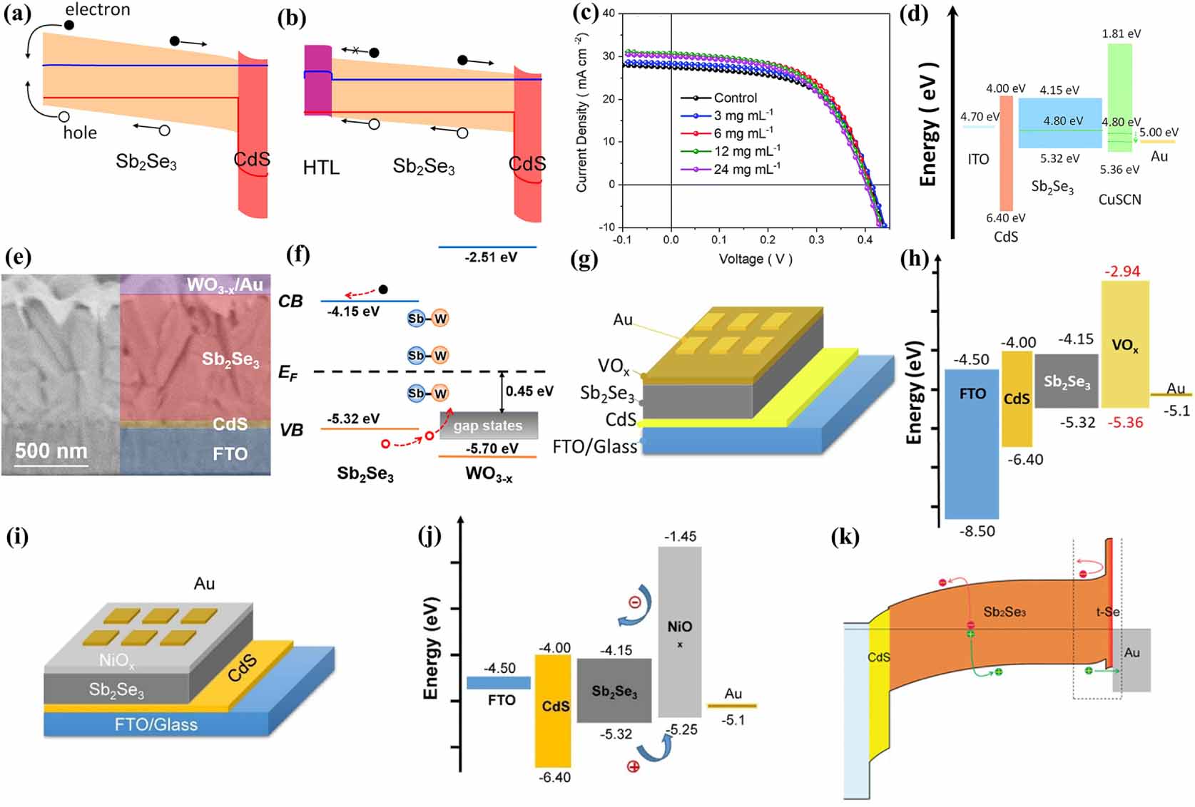
However, the toxicity of certain elements of the above inorganic hole-transporting materials raises concerns about health and environmental pollution in the long-term development, thus calling for the need for environmental-friendly inorganic HTLs. It is therefore that the non-toxic inorganic materials, such as NiOx , are introduced as HTLs in Sb2Se3 PV devices. NiOx has been regarded as a promising inorganic HTL for Sb2Se3 solar cells due to its non-toxicity, large bandgap, and high carrier mobility. Guo and co-workers introduced a 50 nm NiOx into Sb2Se3 solar cells (FTO/CdS/Sb2Se3/NiOx /Au) and improved the cell efficiency from 6.12% to 7.15% (figures 14(i) and (j)). In this work, the NiOx HTL not only reduces the carrier recombination at the Sb2Se3/NiOx /Au interface but also promotes the carrier collection via the proper band alignment [68]. Trigonal selenium (t-Se) is a 1D van der Waals solid with helical atomic chains and it possesses a wide bandgap, high mobility, and high work function, which makes it a promising HTL in planar n–i–p Sb2Se3 solar cells (figure 14(k)). The p-type t-Se layer has proven to promote a favorable band alignment and band bending at the Sb2Se3/t-Se interface, giving rise to the suppression of the interface recombination and enhancement of the hole extraction efficiency [50].
5. Summary and outlook
Although the champion efficiency of Sb2Se3 thin-film solar cells currently lags behind those of other well-developed solar cells, Sb2Se3 has great potential to become a competitive PV technology owing to its proper optical bandgap, high optical absorption coefficient, stable binary phase, earth-abundant constitution, and low toxicity. This review briefly summarizes the basic properties of Sb2Se3 light-harvesting layers, the major progress, and device configurations of Sb2Se3 solar cells, and places particular emphasis on the optimization of energy band alignment from the perspective of interface engineering. Interface quality in Sb2Se3 solar cells is one of the decisive factors that determines the device performance of PV devices. It is therefore of great importance to gain a deep understanding of interface properties and optimize the interface to reduce the defects and carrier recombination in Sb2Se3 devices. A favorable energy band alignment plays a crucial role in determining the device performance of Sb2Se3 solar cells. In this perspective, the optimization of energy band alignments through the application of optimal ETLs and HTLs may pave a way for further improvement in Sb2Se3 solar cells. To optimize the band alignments, it is desirable to apply advanced characterization techniques, such as angle-resolved photoemission spectroscopy and synchrotron radiation photoelectron spectroscopy, for in-depth studies on the energy band alignment between the charge transport layers and Sb2Se3 absorber layer. Furthermore, it is essential to continue the exploration and investigation of new ETLs and HTLs with the help of theoretical calculation. In this review, we summarize various electron and hole transporting materials that have been employed on Sb2Se3 solar cells, trying to provide an insight into the selection of ETLs and HTLs. In addition to the optimization of the interface band alignments, improving the quality of the Sb2Se3 absorber is obviously a must. Various approaches including surface treatments and post-deposition annealing treatments, and dopants incorporation are still under research. The challenge in external doping is that dopants are preferentially incorporated into the 1D ribbons instead of the Sb2Se3 lattice. In this regard, it is necessary to explore the suitable dopants and doping methods and investigate them in depth experimentally and theoretically. Overall, high efficiencies can be achieved by considering the above issues concerning interface and absorber engineering. With the development of advanced technologies, it is foreseeable that continuous investigation of Sb2Se3 will bring us closer to higher PCE and future practical commercial application of Sb2Se3 solar cells.
Acknowledgments
This work was supported by the National Research Foundation of Korea (NRF) grant funded by the Korea Government (MSIT) (Nos. NRF-2018R1A5A1025594 and 2020R1A2C3008111).
Data availability statement
No new data were created or analyzed in this study.