

Abstract
This paper presents research on a novel and modular vertically-integrated wearable skin patch for biosignal measurements. The flexible patch consists of a disposable skin-contacting electrode layer and a durable electronics part. The durable part is designed to include a printed re-chargeable battery, a solar cell, electronics for the measurement of electrocardiogram (ECG), galvanic skin response, acceleration, temperature and humidity and a covering visually appealing jewellery-like functional crystal layer for decoration and user interaction. The patch can store measurement data and transmit it to a mobile phone via a bluetooth low-energy radio. Integration process is developed for the vertical stacking that limits the skin-patch area to achieve a desirable form factor. The sensing electrodes are printed on stretchable thermoformable polyurethane substrate with vias through the substrate to couple skin-contacting electrodes to the upper functional layers. A removable adhesive layer between the disposable and durable parts is developed to enable separating the two parts after wear and then to couple the durable part with a new disposable part. The patch is tested on body for ECG sensing.
Export citation and abstract BibTeX RIS

Original content from this work may be used under the terms of the Creative Commons Attribution 4.0 license. Any further distribution of this work must maintain attribution to the author(s) and the title of the work, journal citation and DOI.
1. Introduction
Wearable skin-mountable sensor patches are typically meant for short-term use such as for a day or a week at a time in applications such as physiological (e.g. sports heart rate), medical (e.g. blood glucose) or mental (e.g. stress) health and wellbeing. For recent reviews on different applications and wearable solutions, see [1–4] especially, the skin-contacting layer of a patch suffers from the wear, becomes dirty and looses its adhesion over long wear times. Therefore, either the whole product needs to enter electronics and battery recycling streams after being used or the skin-contacting layer would need to be renewed. Standard solution is to use a conductive snap connector between a flexible skin-contacting electrode part and a rigid electronics module. However, using the snap connectors limits decreasing the physical size of the product in area and thickness and increasing flexibility of the patch that would be desirable to maximize comfort of wear.
Comfort and desirability of wearing a skin patch is also affected by the overall design and looks of the product, especially, in health and well being applications for appearance-conscious customers. Bulky technical patches become therefore either quickly discarded or worn as concealed under clothing. This would prevent utilization of solar energy harvesting that would be beneficial to avoid use or extend the lifetime of a battery without external charging. The physical appearance therefore in practice influences technical design degrees of freedom and overall environmental footprint of the product.
In this article, a vertically-stacked modular skin patch for chest and arm use is presented that consists of two main parts—a disposable electrode part for single use and a durable reusable electronics part as illustrated in figure 1. The patch includes measurement capabilities for electrocardiogram (ECG) and galvanic skin response (GSR) sensing to be used in sports (ECG-based heart rate) and stress-sensing [5–7] applications. The vertical stacking of the functionalities helps to minimize the area of limited flexibility in the patch and usage of thin-film flexible electronics for the functional layers helps to limit the thickness of the patch. The top layer of the patch is a kind of display with integrated light-emitting diodes (LEDs) for visual, decorative user feedback. The transparent layer allows light to pass through to the solar cell, as well as providing an on-demand ECG measurement control when the patch is worn on the arm. The removable adhesive layer enables exchange of the skin-contacting electrode layer. The skin adhesive is selected such that it enables fast repositioning of the patch in case the patch is put to a wrong location or orientation the first time as indicated by sensing signal quality. Sometimes, the first attach can also fail, for example, if the patch is put on chest in a crouched posture and the patch looses skin contact or stretches skin uncomfortably after straightening. The skin-contacting layer with electrodes, vias and conductor tracks is implemented by screen printing on a thermoplastic polyurethane (TPU) substrate that is stretchable and breathable and can therefore be conveniently extended beyond the area of the upper layers that here have a diameter of 44 mm. The construction of the patch in this article is made in order to test the concepts without yet paying attention to sealing of the structure against moisture, water or other elements.

Figure 1. Structure of the vertically-integrated modular skin patch.
Download figure:
Standard image High-resolution image2. Patch design and manufacturing
The design and manufacturing of the patch is presented layer by layer in what follows.
2.1. Adhesive layers
Adhesives were developed both for attaching the patch to the skin and to enable separation of the disposable part from the durable part to replace the disposable part.
2.1.1. Removable adhesive
The removable adhesive resides between the skin-contacting electrode layer and the electronics layer (PCBA in figure 1) and enables replacement of used disposable part with a new one. The patch is designed for wearing either on wrist or on chest. On wrist, the radius of curvature of the body is significant as compared to the size of the patch whereas on chest, the body is a relatively flat surface over patch-sized areas. Therefore, it is expected that different adhesives should be used for the two use cases to optimize wear durability, comfort (flexibility) and form factor (thickness) of the patch. Different adhesives were tested for their adhesion to a polyimide (PI) substrate representing a flexible printed circuit board assembly (PCBA) and to polyurethane (PU) film representing the skin-contacting layer. The PI contact needed to be strong enough to hold for the duration of wear but not too strong for the users to be able to change the disposable part. For the PU contact, only a strong-enough permanent adhesion was required. Adhesion to PI was tested with peel-force measurements after 10 min, 4 d and 14 d of contact between the layers to find an adhesive that does not bond too strongly even after prolonged time of contact. The wear durability was tested by adhering test patches on a cardboard cylinder surface with 3-inch diameter and monitoring the contact over 20 h (expected period of wear). The test patches consisted of the removable adhesive bonded on one side to a stack of materials shown in table 1 representing the durable part of limited bendability and on the other side to a PU film. The PU film was made larger than the removable adhesive in order to glue it strongly to the cylinder surface using a double-sided tape Tesa 66 825.
Table 1. Durable part replica film stack for adhesion tests that represents the bendability of the actual patch layers.
| Layer | Thickness (μm) |
|---|---|
| PET | 250 |
| Transfer PSA | 50 |
| PET | 250 |
| Tesa 4928 | 125 |
| PET | 250 |
| Transfer PSA | 50 |
| PET | 250 |
| Transfer PSA | 50 |
| PI | 125 |
| Total: | 1400 |
Based on testing several pressure-sensitive adhesives and double-sided tapes, for the chest use, the removable adhesive layer was chosen to be made of a single double-sided tape Tesa 61 528. This tape has a thickness of 100 μm with different adhesives on opposite sides of a polyethylene terephthalate (PET) backing. The silicone adhesive was used to bond to the PCBA PI in a removable fashion and the acrylic adhesive was used to make a permanent contact with the PU film of the skin-electrode layer. For the wrist use case, a stack of materials was selected as shown in table 2. For Tesa 52 060, the peel force in 90° pull from PI was stable at 2 N cm−1 for 14 d while for Tesa 61 528, the peel force increased from 1.8 N cm−1 to 2.5 N cm−1. The target range for the peel force was 1.5–3.5 N cm−1.
Table 2. Removable adhesive for the wrist use.
| Layer | Type (thickness (μm)) |
|---|---|
| Adhesive to PI | Tesa 52 060 (1500) |
| Backing | PET (25) |
| Adhesive to PU | Tesa 66 825 (250) |
| Total thickness: | 1775 |
Figure 2 shows patch test structures detailed in table 3 with two different PU thicknesses and either with or without corona treatment of the PU or PET after attach and after 20 h. The corona treatment was done using a laboratory corona unit (Vetaphone Plus) with distance to substrate of 2 mm, dose of 80 W min m−2, web velocity of 30 m min−1 and electrode width of 0.33 m. The total power on the sample was 792 W. Loss of adhesion between the removable adhesive and the PU was noticed for the thicker (100 μm) PU without corona treatment (samples #4 and #6). For the other samples, the adhesion was sufficient. Figure 3 shows the loss of adhesion between the PU and the removable adhesive as a function of time. For sample no. 4, the lifting starts already after 1 h on the cylinder. The use of the thick foam adhesive for the wrist application and not the chest design was found necessary in on-body user testing to achieve at the same time good adhesion to skin, high wear comfort, low separation of layers and low trauma upon removal.

Figure 2. Patch test structures with 44 mm diameter adhered to a cylinder surface.
Download figure:
Standard image High-resolution image
Figure 3. Lifting between the PU and removable adhesive in test structures of figure 2 as a function of time. Only the PU samples (chest and wrist) with no corona treatment show lifting within 20 h of wear.
Download figure:
Standard image High-resolution imageTable 3. Details of patch structures to test adhesion to curved surface representing the wrist.
| Test no. | 1 | 2 | 3 | 4 | 5 | 6 |
|---|---|---|---|---|---|---|
| Remov. Adh. type | 52 060 | 52 060 | 61 528 | 61 528 | 52 060 | 52 060 |
| PET | PET (+ corona) | PET | PET | |||
| 66 825 | 66 825 | 66 825 | 66 825 | |||
| PU thick. μm | 45 | 45 | 100 | 100 | 100 | 100 |
| PU corona | Yes | No | Yes | No | Yes | No |
| Design | Wrist | Wrist | Chest | Chest | Wrist | Wrist |
2.1.2. Skin adhesive
Preliminary screening of different skin adhesives of several providers was done such that the adhesives were attached to PET and then the PET film with the adhesive was attached to skin followed by removal (after 10 min on skin) using a Zwick tensile tester. The peel force and loss of peel force after repositioning (10 min on skin between first attach and repositioning and another 10 min on skin after second attach before removal) were recorded and the wear comfort was subjectively and visually measured in terms of pain of removal and skin reactions such as redness. Selected adhesives were then worn on body by test persons up to 12 h as shown in figure 4 and evaluated for adhesion, wear comfort and trauma upon removal. In many cases, these requirements are contrary because better skin adhesion typically results in higher trauma upon removal. Therefore, a compromise needed to be found that offers a good balance of the characteristics. Consequently, Ashland Gentle 700E that is compared to two alternative adhesives in figure 5 was selected to be used in the patch.

Figure 4. On body testing of the skin adhesives on wrist (top) and on chest (bottom). Diameter of the semi-rigid center part representing the functional patch area of figure 1 is 44 mm.
Download figure:
Standard image High-resolution image
Figure 5. Results of on-body testing for Ashland Gentle 700E (blue) and two alternatives as subjective rating between 0 (worst) and 100 (best) averaged over the test persons.
Download figure:
Standard image High-resolution image2.2. Skin electrode layer
The skin-contacting layer with measurement electrodes was implemented on a 100 μm-thick clear TPU substrate (Covestro Platilon U073). To make contacts through the substrate, four holes of 300 μm diameter were mechanically punched to the substrate at the center points of skin electrodes. Screen printing by EKRA flat-bed screen printer was then used to implement electrode pads of 6 mm and 8 mm in diameter on the bottom side (facing the skin in the patch) followed by printing of 1 mm wide conductor tracks on the top side simultaneously filling the punched holes to create conducting vias through the substrate. The top-side conductor tracks are used to route the measurement signals such that they can be connected to the bottom of the PCBA as shown in figure 6. The bottom-side electrodes are then overprinted with Ag ink (EMC Cl-1036).
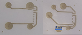
Figure 6. Skin electrode layer versions with 4 (left) and 5 (right) measurement electrodes of 8 mm and 6 mm diameter.
Download figure:
Standard image High-resolution imageThe reliability of the vias and their tolerance against stretching was confirmed by printing test structures consisting of 240 vias in series, measuring their resistance and stretching the samples in tensile tester as shown in figure 7. In total, 72 test structures were fabricated consisting of a total of 17 280 vias out of which only 1 via was not conductive after fabrication. The conductor tracks and vias tolerated high strains up to 100%.

Figure 7. Via test structure (a), strain profile in testing (b) and resistance and force as a function of strain (c).
Download figure:
Standard image High-resolution image2.3. PCBA
The block diagram of the PCBA is shown in figure 8. The power module consists of a perovskite solar cell (PSC), step-up converter to 5 V (maxim integrated MAX17223), battery charger (Microchip Technology MCP73830) and the battery for which a Varta 3.7 V coin cell Li-On battery has been used in this article because a flexible battery that could have been integrated into the patch stack was not available. MUSEIC is the wireless biosensor ASIC of Imec [1] coupled to a ceramic chip antenna (Johnson Technology 2450AT18A100). The ASIC is used to measure ECG and GSR. Two flash memories are used for the program (Microchip Technology SST25WF040) and data storage (Adesto Technologies AT25SL128). The sensors external to the MUSEIC ASIC include a temperature and relative humidity (RH) sensor (Sensirion SHT40) and an inertial measurement unit (Bosch Sensortec BMX160). The LED control is implemented using an input-output (IO) expander (NXP PCAL6416A). The PCBA was implemented both as rigid FR4 and as flexible PI board. The testing of this article focuses on using the rigid FR4 boards shown in figure 9. The three rectangular extensions of the board are for programming, debugging and data readout during development and they are meant to be finally cut off.

Figure 8. Block diagram of the PCBA.
Download figure:
Standard image High-resolution image
Figure 9. Assembled PCBA. The wires are for external power source.
Download figure:
Standard image High-resolution image2.4. Battery layer
Above the PCBA is the battery layer for which a printed flexible rechargeable battery with a total thickness of less than 600 μm was developed. The active battery materials are embedded between a bottom and a top substrate. The bottom and top substrates are sealed tightly with an adhesive around the circumference of the battery materials. The inside of the battery stack is shown in figure 10.

Figure 10. Stack design of the rechargeable battery.
Download figure:
Standard image High-resolution imageThe entire stack is screen printed using an EKRA E2 press. The current collectors at the bottom and top consist of a silver layer for lowest possible resistance and are each covered by a passivating carbon black layer to avoid negative influence of the silver on the electrochemistry. The contacting with the PCBA was realized with a riveting system from Bungard 12 . The solderable copper rivets (1.2 mm diameter) are applied manually in the outer sealing area of the printed battery of circular shape shown in figure 11. The stack layout is typical for printed batteries, only the electrochemical systems of the anode, cathode and electrolyte are varied as needed. For a rechargeable battery, a Li-Ion-system with a nominal cell voltage of 3.7 V was used. As a combination of separator and electrolyte, a printable but porous membrane of polyvinylidene fluoride was investigated. The membrane was soaked in electrolyte where a gel then forms. First proof-of-concept in a CR2032 cell format showed a performance for the developed gel-membrane that is comparable to a commercial separator (see charge and discharge curves in figure 12). Moreover, to avoid the use of hazardous solvents, water-born printing pastes for anode and cathode have been developed.
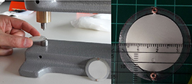
Figure 11. Placing the rivets (left) and printed battery with rivets as contacts (right).
Download figure:
Standard image High-resolution image
Figure 12. PoC of PVdF-Membrane [blue] vs. a commercial battery separator [red] using similar electrodes in a CR2032 coin cell setup.
Download figure:
Standard image High-resolution imageThe difficulty with Li-Ion-systems is that the electrolyte must be handled in an ultra-dry environment. Therefore, the production concept was designed to produce all components under ambient atmosphere, with only the final steps of electrolyte impregnation and laminating to be performed under dry conditions. During the project, it could be shown that the chemical system works in principle but a printed battery in the required circular form factor shown in figure 11 could not be completed in time. Therefore, an external VARTA Li-Ion coin cell was used for testing purposes.
In addition, studies on substrate properties (e.g., barrier properties for low water vapor permeability to prevent the battery from drying out) and mechanical tests, such as the bending stiffness of the battery cells, have been carried out and are described in [8].
2.5. Perovskite photovoltaic
For recharging the battery using light energy, flexible perovskite-based solar cell PSC module was developed on PET/indium tin oxide (ITO) substrate (see figure 13). The PSC technology was selected due to its high optical absorption under indoor lighting conditions. The PSC module is arranged in a so-called inverted p-i-n architecture in which the PET/ITO/hole transport layer (HTL) is used as substrate and transparent anode and electron transport layer (ETL)/Cu as metallic cathode [9, 10]. The module has an aperture area of 9.08 cm2. The active area is 8.3 cm2 (GFF ∼91%). To be compatible with the circular patch design and to provide a 4 V charging voltage, the PSC module was also made circular with five sub cells of equal 1.82 cm2 area connected in series. Since each sub-cell generates about 1 V under one sun light illumination, the output voltage of the module will be high enough even in much lower light intensities such as indoor conditions. A picosecond (ps) ultraviolet (UV) laser was used to pattern the large area circular-shaped module into five individual sub-cells and implement the monolithic series interconnection of the cells [11]. The HTL and double-cation perovskite (Cs0.18FA0.82PbI2.82Br0.18 with 1.6 eV bandgap) layer are processed from solution by spin coating. The perovskite layer undergoes a (Nitrogen) gas quenching (drying) and an annealing step after the spin coating. The ETL and metallic Cu top electrode are deposited by thermal evaporation. The total width of the loss area due to laser scribes is typically in the order of 450–500 μm. The same ps UV laser is used to cut the circular shape out of the initially squared substrate. It must be noted that the series monolithic interconnection of sub-cells in a module is commonly used in thin film PV module processing, often in a rectangular shape [11, 12], but the customized circular shape and module geometry using a flexible substrate here is to the best of our knowledge unique.
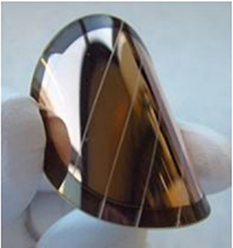
Figure 13. Flexible perovskite photovoltaic.
Download figure:
Standard image High-resolution image2.6. Display layer
The display layer consists of the decorating crystal film and the LED light film as follows.
2.6.1. Crystal film
To have an appealing look for the patch, the top surface is implemented using decorating Swarovski crystals that are assembled on PET film (Melinex ST506) using a transparent UV gluing system. The center crystal was made electrically conductive by ITO coating applied in a sputtering process [13] to be able to measure ECG even if the patch is worn on arm by connecting a finger of the other hand to the patch. The rest of the crystals are designed to effectively pass the LED light out to be seen by the user and the sun light in to be harvested by the solar cell [14]. Figure 14 shows the film with two different colors used for the crystals.

Figure 14. Crystal film with two different crystal colors (left: green & right: blue). The center crystal of the right crystal film is the ITO-coated conductive crystal.
Download figure:
Standard image High-resolution image2.6.2. LED film
The display layer is implemented on 125 μm thick PET substrate (Melinex ST506). Conductor tracks are fabricated onto the substrate by screen printing (EKRA) using (Asahi 411AW) silver ink. The conductor tracks are printed on both sides of the substrate such that tracks on the same side of the substrate do not cross. The wirings at both sides are connected by vias that are fabricated using the same process as for the skin-electrode layer discussed above. The display is designed in order to show different symbols as illustrated in figure 16. The symbols consist of 40 light dots in total. At the location of each dot there is a decorative crystal element in the crystal layer. The light dots are implemented using red and green LED dies (Epistar ES-AEHRAX12 and ES-CEGHV15B, respectively) (80 dies in total) that are assembled onto the substrate by anisotropic-conducting-adhesive bonding using Datacon 2200 EVO assembly machine and Delomonopox AC265 adhesive by Delo. The red and green LED chips have areas of about 300 μm × 300 μm and 380 μm × 380 μm and a thickness of about 100 μm and 90 μm, respectively. The display layout design together with the decorative element layout and the assembled LED film are shown in figure 15. To limit the complexity of the wiring for the control of the LEDs to illuminate the display symbols, the patch was designed to be able to show the five symbols shown in figure 16. The electrode in figure 15 at the center of the patch is used to connect the conductive crystal and the electrodes from about 8 o'clock to 10 o'clock are used to connect the LED film to the PCBA using rivets.

Figure 15. LED film and crystal-film layouts (left) and assembled LED layer (right).
Download figure:
Standard image High-resolution image
Figure 16. Display symbols.
Download figure:
Standard image High-resolution image2.7. Patch integration
The disposable-part and durable-part layers were integrated with the PCBA as follows.
2.7.1. Disposable part integration to the PCBA
Integration of the disposable part to the PCBA started by equipping the PCBA bottom contacts with rivets, which were solder bonded to the PCBA contact pads. Anisotropic conductive gold-ion-silicone elastomer (Shenzen Brilliance Rubber) with thickness of 150 μm was then laminated over the rivets. Openings were cut to the removable adhesive layer to couple electric bio-signals to the PCBA bottom contact pads. Openings were cut using ELAS UV laser and the removable adhesive was laminated in the PCBA bottom as shown in figure 17. Next, the skin-electrode layer was laminated onto the removable adhesive such that electrical connection was created from the PCBA bottom contacts to the measurement electrode contact points at the top surface of the skin-electrode layer. After that, the skin adhesive with laser cut (ELAS UV laser) openings for the electrode areas was laminated onto the skin-electrode layer. Finally, hydrogel (Axelgaard AG625) was cut to the shape of the electrodes and manually placed over the electrodes. The bottom liner of the hydrogel was left in place until the patch was to be attached to skin. Figure 18 shows the disposable part integrated with the PCBA. The white liner of the skin adhesive is partly lifted to show the contacting area.

Figure 17. Removable adhesive with openings laminated in the PCBA bottom. Openings are at the location of the PCBA bottom contact points that are equipped with rivets and covered with anisotropic conductive elastomer pieces.
Download figure:
Standard image High-resolution image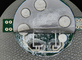
Figure 18. Disposable part integrated to the PCBA.
Download figure:
Standard image High-resolution image2.7.2. Durable part integration
The PCBA top surface contacts were coupled to the upper functional layers using thin wires that were bonded using isotropic conductive adhesive (ICA, EPO-TEK H20E) to the PSC and LED display and then soldered to the PCBA. Alternatively, the same method with rivets and conductive elastomer as used for the disposable part could be used.
The PCBA top surface was partially planarized using insulating double-sided foam tape (TESA 62 936) as shown in figure 19. The wires shown in figure 19 are for connecting an external power source. The PSC and LED display were laminated together using nonconductive film (NCF, TESA 69 401) and then they were laminated on top of the PCBA as shown in figure 20. The crystal film was laminated on top of the LED display using the same NCF as shown in figure 21. The conductive crystal at the center of the crystal layer was bonded to the LED layer using ICA (EPO-TEK H20E). Electrical contacts in the patch were tested using digital multi-meter measurements. Resistance from the center crystal to the PCBA via the LED film was 80 Ω (see figure 22) and resistance from skin electrodes to the PCBA varied between 2 and 5 Ω, when the skin-electrode layer was repeatedly changed to a new one. The variation can be explained by alignment error between the contacts of the layers.

Figure 19. PCBA equipped with planarizing foam.
Download figure:
Standard image High-resolution image
Figure 20. Patch with LED and PSC layers integrated.
Download figure:
Standard image High-resolution image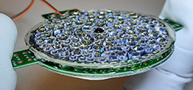
Figure 21. Crystal film integrated to the patch completing the structure.
Download figure:
Standard image High-resolution image
Figure 22. LED display showing the heart symbol and measurement for the resistance from the conductive crystal to the PCBA.
Download figure:
Standard image High-resolution image3. Testing
3.1. Perovskite photovoltaic
The circular flexible photovoltaic modules consisted of five cells in series. After fabrication, the modules were stored in inert atmosphere in glove box filled with nitrogen because under normal room atmosphere, oxygen and humidity exposure causes modules to degrade. The modules were characterized under one sun illumination (100 mW cm−2) using solar simulator.
The results for six modules that were used in patch integration are shown in table 4. On the average, the modules had a short-circuit current (Isc) of 19.22 mA, open-circuit voltage (Voc) of 5.15 V, fill factor of 57.9%, short-circuit current density (Jsc) of 2.12 mA cm−2, power conversion efficiency (PCE) of 6.32% and maximum power (Pmax) of 57.37 mW. The variation between the modules was due to lack of optimization of the process. The flexible substrate could curve during spin coating or gas quenching, causing inhomogeneities in the resulting film. Although not reaching the state-of-the-art performance for flexible photovoltaics in terms of PCE [15], the available power would still be of importance for the targeted use cases.
Table 4. Perovskite solar cell measurement results. The module area is 9.08 cm2.
| PSC# | Isc (mA) | Voc (V) | FF (%) | Jsc (mA cm−2) | PCE (%) | Pmax (mW) |
|---|---|---|---|---|---|---|
| 1 | 19.58 | 5.28 | 54.50 | 2.16 | 6.20 | 56.31 |
| 2 | 19.51 | 5.34 | 57.86 | 2.15 | 6.64 | 60.28 |
| 3 | 18.87 | 4.59 | 53.68 | 2.08 | 5.13 | 46.54 |
| 4 | 19.21 | 5.23 | 61.42 | 2.12 | 6.80 | 61.71 |
| 5 | 19.13 | 5.30 | 59.92 | 2.11 | 6.69 | 60.71 |
| 6 | 19 | 5.14 | 60.03 | 2.09 | 6.46 | 58.67 |
| Mean | 19.22 | 5.15 | 57.90 | 2.12 | 6.32 | 57.37 |
| Std | 0.28 | 0.28 | 3.17 | 0.03 | 0.62 | 5.63 |
Figure 23 shows the measured Jsc–Voc characteristics of the PSCs.

Figure 23. Current-voltage characteristics of the PSCs.
Download figure:
Standard image High-resolution image3.2. Decorative layer
The functionality of the LED display layer was verified in a test bench as shown in figure 22. The test bench is comprised of two polycarbonate plates. Upper plate has an opening for the LED display active area that consists of bare LED dies. Upper plate alto contains electrical contact pins for display testing. Display testing started by placing the sample between the plates and aligning the sample so that all required contact pins were aligned to the sample contact points. Alignment of the sample was then secured by fixing the sample and plates using four pins.
Four of the photovoltaic modules were tested in a sun simulator under one sun illumination with the decorative layer on top as shown in figure 24. The results are shown in table 5 and in figure 25. About half of the available power is lost due to covering the photovoltaic. Consequently, for the estimated power consumption of the patch electronics, the photovoltaic can charge the needed energy into the battery for daily consumption in 15 min under one sun illumination to enable 2 min ECG measurements every 15 min, 12 times LED user feedback for 20 s and blue-tooth data transmission once a day. The decorative layer was also tested outdoors as shown in figures 26 and 27.

Figure 24. PSC measured in a sun simulator with the crystal and LED film on top.
Download figure:
Standard image High-resolution image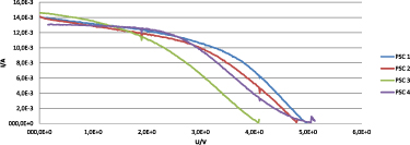
Figure 25. Current-voltage characteristics of the photovoltaics with the decoration layer on top.
Download figure:
Standard image High-resolution image
Figure 26. Open-voltage measurement in the sun.
Download figure:
Standard image High-resolution image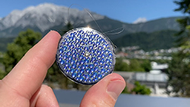
Figure 27. Decorative layer prototype in sunlight at Swarovski factory (Austria).
Download figure:
Standard image High-resolution imageTable 5. Photovoltaics measured in sun simulator with the decoration layer.
| PSC# | Isc (mA) | Voc (V) | Jmpp (mA cm−2) | Vmpp (V) | PCE (%) | Pmax (mW) |
|---|---|---|---|---|---|---|
| 1 | 14.1 | 4.98 | 1.1 | 3.39 | 3.62 | 32.8 |
| 2 | 14.1 | 4.80 | 1.1 | 3.07 | 3.31 | 30.0 |
| 3 | 14.6 | 4.09 | 1.1 | 2.32 | 2.56 | 23.2 |
| 4 | 13.1 | 5.12 | 1.2 | 2.73 | 3.28 | 29.8 |
| Mean | 14.0 | 4.75 | 1.1 | 2.88 | 3.19 | 29.0 |
| Std | 0.6 | 0.46 | 0.06 | 0.46 | 0.45 | 4.1 |
3.3. PCBA laboratory testing
ECG measurement functionality of the skin patch was confirmed with an ECG simulator (MedTec & Science GmbH MS410) coupled to the measurement electrodes. The waveform was transferred to a mobile phone via a bluetooth low energy (BLE) radio connection (see figure 28). A low sampling rate of 32 samples per second was used to facilitate data buffering and communication between the un-optimized patch firmware and phone app.

Figure 28. A measurement test result using an ECG simulator. The data was transferred to a mobile phone via BLE.
Download figure:
Standard image High-resolution imageGSR measurement functionality was confirmed by manually connecting different fixed resistors to the GSR input of the skin patch that represent the typical GSR signal levels [16]. Data transfer was done via BLE (see figure 29).

Figure 29. Result of a GSR measurement where fixed resistors of different values were inserted to the GSR input. Here, the resistance at the GSR input decreases from 1.2 MΩ to 100 Ω and then increases back to 1.2 MΩ.
Download figure:
Standard image High-resolution image3.4. On body testing
The patch was tested on body in the wrist (arm) and chest use cases. Due to the low sampling rate of 32 samples per second, the short distance (∼45.5 mm center to center) between the small measurement electrodes (∼8.3 mm diameter) and possibly un-optimal contact with the skin especially for the wrist/arm use case, the signal quality was too low to detect other ECG signal characteristics than the heart rate.
3.4.1. Wrist use case
Figure 30 shows the patch attached to the inside arm a test person at rest in sitting position. External power source is used that is coupled to the patch using the wires visible in the picture. The measured and transmitted data is illustrated in figure 31 and a calculated power spectrum in figure 32. The heart rate of 76 beats per minute (bpm) can be obtained as the largest peak of the power spectrum.

Figure 30. Patch on arm for ECG measurement with a finger from other arm touching the center crystal.
Download figure:
Standard image High-resolution image
Figure 31. Snapshot of the ECG data (arbitrary units) from the arm measurement.
Download figure:
Standard image High-resolution image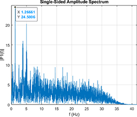
Figure 32. FFT power spectrum of the ECG data of figure 31. The largest peak is at 1.27 Hz = 76 beats per minute.
Download figure:
Standard image High-resolution image3.5. Chest use case
Figure 33 shows the patch attached on the chest of a test person staying still in standing position. The external battery is used to provide supply power for the patch. The measured and transmitted data and the corresponding calculated power spectrum are shown in figures 34 and 35, respectively. The signal quality is better than for the wrist use case. The lowest-frequency high peak of the power spectrum corresponds to the heart rate of 78 bpm.
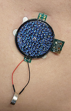
Figure 33. Patch on chest for ECG measurement with external battery. The patch location is on top of the lower ribs next to solar plexus on the left side. The ECG measurement electrodes are leftmost and rightmost ones in the picture. The rightmost measurement electrode is under the programming slip and therefore not visible.
Download figure:
Standard image High-resolution image
Figure 34. Snapshot of the ECG data (arbitrary units) from the chest measurement.
Download figure:
Standard image High-resolution image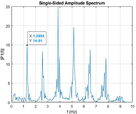
Figure 35. FFT power spectrum of the ECG data of figure 34. The leftmost peak is at 1.3 Hz = 78 beats per minute. The other peaks are higher harmonics of the 1.3 Hz peak.
Download figure:
Standard image High-resolution image
4. Conclusions
A new structural concept of a vertically-stacked wearable patch was reported that consist of disposable and durable parts that are coupled together using conductive adhesives. The patch includes separate layers for (i) an outermost decorative signage layer with functional crystals and LEDs to improve user acceptance, (ii) a flexible perovskite photovoltaic to extend use time without external charging, (iii) a rechargeable battery, (iv) electronics PCBA, (v) removable adhesive layer between the disposable and durable parts, (vi) skin electrodes implemented on TPU and (vii) skin adhesive. The patch is equipped to measure ECG, GSR, temperature, RH and acceleration. The patch parts were developed and tested separately and an integrated patch was tested on body for ECG sensing both for wrist and chest use cases with non-moving test person. Heart rate and heart-rate variance could be detected for both use cases with better signal quality obtained in the chest use case.
Novelty of the approach is demonstrated in terms of the overall design with vertically stacked flexible/bendable durable and disposable parts that are bonded together using an adhesive that is developed for the purpose. Typically, vertical designs with replaceable parts use snap-button connectors between rigid parts or place components laterally that consumes more area [17]. The overall design also approaches a jewellery-like appearance increasing the user acceptance of the solution also for uncovered skin areas that is important for the solar powering. The developed materials combination enables the removable adhesive and the skin adhesive to work together such that the removable adhesive is sufficiently stronger than the skin adhesive for the patch to not break apart when detached from skin but not too strong to prevent changing of the skin-electrode layer. For the stretchable and breathable TPU substrate acting as the skin-contacting layer, reliable vias are developed. Other point of novelty include (i) usage of Imec's non-commercial Museic ASIC as the main chip, (ii) concept for a new battery solution is presented although not being used in the integrated patch, (iii) the functional decorative layer with functional crystals and LEDs integrated together with the flexible perovskite photovoltaic and (iv) the integration process to combine all functions (except the battery) into a patch.
Future work will focus on (i) fabrication of skin contacting layers with larger electrode separation and larger electrodes for better signal quality, (ii) SW and HW improvements to enable higher sampling rates, (iii) developing further the flexible battery technology and integrating it into the stack, (iv) sealing of the patch structure against water ingress, (v) optimizing the LED assembly process to improve the yield, (vi) motion artefact cancellation, (vii) on-body GSR and acceleration measurements (viii) measurements during motion and (ix) increasing the usage of printing in fabrication.
We believe that our results contribute to development of smart wearable patches for new applications in monitoring both physical exercise and mental wellbeing/stress in use cases where an appealing design should positively contribute to user acceptance. Examples of such applications can be found, for example, at the interface of electronics and jewellery markets like promoted by Swarovski [18]
Acknowledgments
This work has received funding from the European Union's Horizon 2020 research and innovation programme under Grant Agreement No. 825172 (BEWELL project).
Data availability statement
All data that support the findings of this study are included within the article (and any supplementary files).