
Abstract
In this article, an interfacial conductivity model for the surface potential and the drain current was proposed based on the metal-interface-ferroelectric-insulator-semiconductor (MIFIS) structure negative capacitance field effect transistor (NC-FET). The simulating results illustrate that the electrical conductivity (σ) of the interface layer between the electrode and ferroelectric thin film caused by lattice misfit plays an important role in the process of voltage amplifying and steep switching for the NC-FET. It is indicated that new device design rules should take into account this scenario.
Export citation and abstract BibTeX RIS

Original content from this work may be used under the terms of the Creative Commons Attribution 4.0 licence. Any further distribution of this work must maintain attribution to the author(s) and the title of the work, journal citation and DOI.
With the development of Moore's law, the feature size of semiconductor devices has been continuously reduced, which has increased the power density of integrated circuits and the operating temperature of chips while the reliability and performance have been greatly reduced [1]. Reducing the subthreshold swing of the transistor is an effective way to reduce the voltage and power consumption of the integrated circuit. As early as 2008, Salahuddin and Datta [2] proposed to use ferroelectric thin film to replace the insulating material in the traditional MOS transistor to form an MFS structure, and such transistor with a negative capacitance can decrease the subthreshold swing (SS) below the physical limitation (60 mV/dec), thus a device with low power consumption can be realized. The subthreshold swing is numerically equal to the gate-source voltage required to increase the subthreshold current by an order of magnitude. The smaller the value of the subthreshold swing is the stronger control of the gate-source voltage imposes on the subthreshold current in the channel [3]. Equation (1) is the expression of subthreshold swing.

At room temperature, the value of (kT/q)ln10 term is about 60 mV/decade, so how to make SS smaller than 60 mV/decade depends on the value of (1 + Cs/Cox) term, where Cs is the capacitance of semiconductor silicon, while Cox is the insulator capacitance. Since the theory of negative capacitance was proposed, many researchers have conducted a large number of theoretical and experimental studies [4–12]. In these studies, Hoffmann et al [7] proposed that defects, charge trapping, and electric field-induced structural changes need, in particular, to be investigated in greater detail in the NC-FET devices. Previous studies [13, 14] showed that the conductivity of the interface layer between the ferroelectric layer and the electrode caused by the failure of the lattice matching can be used as an intermediate parameter to link the lattice mismatch. Based on this idea, in this article, we propose a theoretical model to describe the influence of intermediate variable electrical conductivity on the electrical characteristics of the NC-FET, focusing on the voltage amplification factor and the subthreshold characteristics. It is expected that this study can provide some useful guidelines for the design of low power dissipation of the NC-FETs.
First, the electric displacement D formula in the MIFIS structure (as shown in figure 1(a)) can be given as follows


Figure 1. (a) Schematic diagram of MIFIS-FET structure; (b) Equivalent capacitance divider.
Download figure:
Standard image High-resolution imageWhere ε0 is the vacuum permittivity, εi is the dielectric constant, Ei is the electric field, and Pi is the polarization. The subscripts f and i represent the ferroelectric layer and the interface layer between the electrode and the ferroelectric layer, respectively. Figure 1(b) is the equivalent capacitance divider of the MIFIS structure. The Ci' is the capacitance of the interfacial layer between the metal electrode and the ferroelectric. Cf stands for the capacitance of the ferroelectric layer. Ci is the capacitance of the insulator layer between the ferroelectric and the semiconductor. Cs stands for the semiconductor capacitance. Given the current continuity between the ferroelectric layer and the interface layer, the total current density satisfies the following equation

Where J is the current density, σi and σf represent the conductivity of the interface layer and the ferroelectric layer, respectively. D' represents ∂D/∂t. To avoid complicated calculations caused by time t, an external triangular electric field is employed, and the value of ∂Ef /∂t takes +1 or −1 when the electric field is increasing or decreasing [13]. According to the Landau-Khalatnikov (LK) theory, for a nonlinear ferroelectric capacitor, the relationship between the Gibb's free energy (U) and ferroelectric polarization (P) can be expressed as [15–17]

Where

Ef
is the electric field across the ferroelectric layer, and α, β, and γ are called Landau parameters. For simplicity, the steady-state polarization was considered and  was assumed in equation (4). Combining equations (4) and (5), one can get the ferroelectric electric field.

Equation (6) can be further expressed as.

According to the previous derivation reported by Salahuddin [2], equation (7) can be rewritted as

In equation (8), Q is the charge density of the combination of layers for the series capacitor. In this work, we assume Y-HfO2 as the ferroelectric material [18, 19], which is characterized by the Landau parameters α = −1.23 × 10⁹ m F−1, β = 3.28 × 10¹⁰ m5F−1C−2, and γ = 0 (as shown in figure 2). Ignoring the interface trap and space charge, the gate voltage applied to the MIFIS structure can be described as.

Where, Vint = Qtint /(ε0 εint), Vins = Qtins /(ε0 εins) are the voltage drops of the interface.

Figure 2. Landau parameters α, β, and γ are extracted by fitting the Landau curve to the polarization versus voltage hysteresis curve as reported in the previous references [18, 19].
Download figure:
Standard image High-resolution imageLayer and the insulator layer, respectively. φs stands for the silicon surface potential. tf , tint , and tins are the thickness of the ferroelectric layer, the interface layer, and the insulator layer, respectively. According to Sze's model [20], Q can be described as the function of φs.

IN equation (10), LD = (εs /qNa λ)1/2 is the Debye length, Na the majority carrier concentration, and ni the intrinsic carrier concentration. λ can be calculated by λ = q/kT, where k is the Boltzmann constant, T is the absolute temperature, and q is the electronic charge. According to Pao and Sah's model [21], the current from source to drain in MIFIS-FET can be expressed as.

WHERE φB = (Kt/q)ln(Na /ni), while the electric field ξ(φs, V) can be expressed as [21]

From the equations (2)–(12), one can get the curves of Vg -φs and Vg -IDS of the MIFIS structure field effect transistor.
In the process of simulation, we assumed four different ferroelectric layer thicknesses tf = 4, 6, 8, 10 nm, the thickness ratio is υ = tint /tf = 0.1. The most obvious amplification effect of silicon surface potential can be observed at tf = 8 nm when the interfacial conductivity is 0.035 × 10⁻¹¹ Ω−1m−1, which is shown in figure 3(a). As a general rule, big value of tf gives rise to hysteretic phenomenon. When tf reduces, the hysteresis disappears, and the voltage amplification effect can be obtained. The result is consistent with the previous results reported by Salahuddin [2] and Jiménez [22]. For better understanding the surface potential amplification effect, the voltage amplification factor defined as G = ∂φs/∂Vg, which is present in figure 3(b). The maximal value of G (bigger than 10) for the case of tf = 8 nm appears when the gate voltage is about 0.52 V. For small values of tf , the voltage amplification capability vanishes.

Figure 3. (a) The relationship between the silicon surface potential and gate voltage, and (b) the relationship between the voltage amplification coefficient G and gate voltage with different ferroelectric thicknesses.
Download figure:
Standard image High-resolution imageIn order to prove the voltage amplification effect can be used as a way of obtaining steep subthreshold slope, we calculated the drain-source current versus the gate voltage (ID-Vg) characteristic in figure 4. Where, the interfacial conductivity is assumed to be 0.035 × 10⁻¹¹ Ω−1m−1. Four different ID-Vg curves corresponding the ferroelectric film thickness of 2 nm, 4 nm, 6 nm, and 8 nm for the NC-FET were shown. From figure 4, one can see that the best subthreshold characteristic is the case of 8 nm, which means the maximal G in the MIFIS structure automatically translates into SS < 60 mV dec−1 in the transfer characteristic. It is indicated that tuning tf properly is a key part of the NC-FET device design.

Figure 4. The transfer characteristics with different ferroelectric thicknesses tf = 2 nm, 4 nm, 6 nm and 8 nm.
Download figure:
Standard image High-resolution imageIn actual devices, due to the mutual diffusion of atoms between the electrode material and the ferroelectric thin film, an interface layer will inevitably be formed under the action of heat and electricity, and the electron transport ability of this interface layer can be attributed to the electrical conductivity (σ). For the purpose of investigating the effect of σ on the electrical characteristic of the NC-FET, we firstly calculated the changes of silicon surface potential with the gate voltage under different values of interface electrical conductivity, which is present in figure 5(a). Where, tf = 8 nm, and the value of σ changes from 0.015 × 10⁻¹¹ Ω−1m−1 to 0.055 × 10⁻¹¹ Ω−1m−1. Interestingly, small-σ values result in hysteretic behavior. When σ increases, hysteresis disappears, and G ≫ 1 can be obtained, the biggest value of G appears at σ = 0.035 × 10⁻¹¹ Ω−1m−1, which is shown in figure 5(b). Actually, this phenomenon can be understood like this. According to figures 3(b) and 5(b), for tf = 8 nm, the biggest G appears at σ = 0.035 × 10⁻¹¹ Ω−1m−1. Smaller values of the interfacial conductivity mean that the behavior of the interfacial layer is closer to the ferroelectric layer, indicating the effective thickness of the ferroelectric is increased, so small values of σ result in hysteretic behavior. While, bigger values of the interfacial conductivity indicate the behavior of the interfacial layer is more different from the ferroelectric layer, which mean there is a reduction of effective thickness of ferroelectric layer, thus bigger values of σ enable the voltage amplification effect to vanish, which is similar to the thickness effect as shown in figure 3. It is worth noting that the effect of σ is more obvious than that of tf . The result illustrated that there is an optimal σ which enables the voltage amplification factor to be maximal when tf = 8 nm, which may provide useful guidelines for designing the NC-FETs as logic devices.
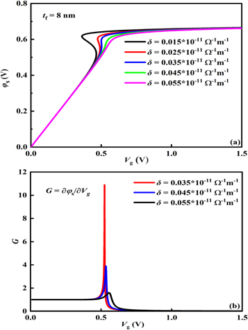
Figure 5. (a) The relationship between the silicon surface potential and gate voltage, and (b) the relationship between the voltage amplification coefficient G and gate voltage with different conductivity of interface.
Download figure:
Standard image High-resolution imageFigure 6 shows the effect of interface electrical conductivity on the transfer characteristics of the NC-FET, and three ID-Vg curves with typical electric conductivity values of σ = 0.035 × 10⁻¹¹, 0.045 × 10⁻¹¹ and 0.055 × 10⁻¹¹ Ω−1m−1 were computed. Where, the thickness of Y-HfO2 ferroelectric thin film was assumed to be tf = 8 nm. From figure 6, for the case of σ = 0.035 × 10⁻¹¹ Ω−1m−1, one can clearly see that the subthreshold slope is the steepest one, corresponding the biggest G in figure 5(b).
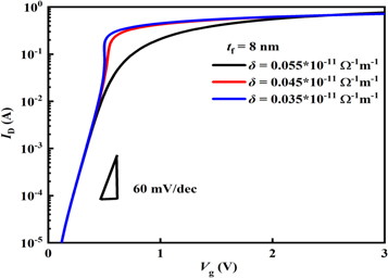
Figure 6. The transfer characteristics with different conductivity of interface.
Download figure:
Standard image High-resolution imageThat is to say, for a certain tf , there is an optimal σ enabling the voltage amplification factor to be the biggest and the subthreshold swing to be the smallest. For better to see the changes of SS with the gate voltage, we plotted the SS-Vg curve in figure 7. Where, tf = 8 nm, and σ = 0.035 × 10⁻¹¹ Ω−1m−1. It can be seen that the smallest value of SS is 27 mV dec−1 when the gate voltage is about 0.5 V. This property can provide reference for the design and performance improvement of the NC-FETs.

Figure 7. The changes of subthreshold swing with gate voltage for the case of tf = 8 nm, and σ = 0.035 × 10⁻¹¹ Ω−1 m−1.
Download figure:
Standard image High-resolution image
In summary, an surface potential and drain current model considering the interface layer with an electric conductivity between the ferroelectric thin film and electrode was proposed in the MIFIS structure based on the Landau-Khalatnikov (LK) theory, Poisson equation, and current continuity equation. The influences of the conductivity on the Vg-φs characteristics, G-Vg characteristics, and Ids-Vg characteristics of the negative capacitance FET were simulated. The results showed that there is a best value of the electric conductivity for obtaining the maximal voltage amplification factor and the steepest subthreshold slope in the NC-FET, and the interface conductivity has a considerable influence on the electrical properties of the NC-FET. It was suggested that more attention should be paid to the arts and crafts of the NC-FET devices. Further work based on the TCAD simulation should be carried out [23, 24].
Acknowledgments
The authors would like to thank the financial supports from the National Natural Science Foundation of China under Grant Nos. 51872250, and 11835008, the technology innovation leading plan (Science and technology tackling) project of Hunan Provincial new and high-tech industry under Grant No. 2020GK2052, the Foundation of Innovation Center of Radiation Application (KFZC2018040201) and the State Key Laboratory of Intense Pulsed Radiation Simulation and Effect (Northwest Institute of Nuclear Technology) under Grant No. SKLIPR1814, the Key Project of Scientific Research Fund of Hunan Provincial Education Department (Grant No. 19A473), and the Key Laboratory of Low Dimensional Materials & Application Technology of Ministry of Education (Xiangtan University) under Grant No. KF20180203.
Data availability statement
The data that support the findings of this study are available upon reasonable request from the authors.
Conflict of interest
The authors declared that they have no conflicts of interest to this work.