

Abstract
Transition Metal Dichalcogenides (TMDs) holding a graphene like 2D structure, offer a vast area of applications in nanoscale electronics. TMD based on MoS2, was thermally grown on ITO coated substrate to perform as a transparent switching layer. The structural and chemical properties of as synthesized MoS2 nanoparticles and thin films have been studied by using x-ray diffraction analysis and scanning electron microscopy, while memory application is manifested by fabricating Al/MoS2/ITO devices. Detailed electrical characterizations suggested that the device shows bipolar resistive switching with low operating voltage, multilevel capability, long retention capacity, presenting its potential as an application in high-density data storage field. In addition, the excellent photo-response capability of the device enriches its execution in light sensing electronic devices along with the resistive switching property.
Export citation and abstract BibTeX RIS
Introduction
Recently, resistive switching (RS) phenomenon is an area of interest due to the immense ability for holding all the desired merits, in the field of nonvolatile memory industry. The simple metal–insulator–metal (MIM) structure with enhanced read/write speeds and low power consumption properties of the switching device has attracted a pronounced attention in the scientific community [1–5]. RS devices, works on the principle of resistance shift from a high resistance state (HRS) to a low resistance state (LRS) upon the application of an external electric field, which regulates the conductive pathways in the active material [6–8]. To date, the RS property has been witnessed in many semiconducting and insulating materials. Consequently, numerous models have been suggested, including the metal-insulator phase transition [9], the ferroelectric polarization [10], and the conductive bridge built by the relocation of localized metal atoms or defects [11] and the RS mechanisms are still being discussed [5, 12]. In past few years, the conventional silicon semiconductor is being replaced by graphene in electronic devices and chemical sensors because of its high carrier mobility and sensitivity to environmental charges [13, 14]. However, the zero energy gap of graphene impedes its use in logic electronics [15]. Recently, great attention have been focused on TMDs due to their two-dimensional (2D) layer structure similar to graphene. Out of which molybdenum disulphide (MoS2) emerges as a potential contender for electronic and optoelectronic applications. In MoS2, molybdenum (Mo) and sulphur (S) atoms are coordinated in a triangular prismatic fashion to provide graphene like structure and the S–Mo–S sandwiches are stuck together by weak Van-der-Waals forces [16, 17]. MoS2 has attracted great interest due to its implementation in various electronic devices, such as field-effect transistors (FET) [18, 19], integrated circuits [19, 20], phototransistors [21, 22] and so on. Moreover, MoS2 based atomic layer transistor shows high carrier mobility and superb on/off current ratio, which makes it suitable for the nonvolatile switching memory device [23]. Meanwhile, a change in the band gap from indirect to direct one is observed upon the reduction in dimension from a bulk form to a 2D monolayer sheet. Consequently, alteration in electronic and optical properties is also discussed [24–26].
In this paper, we report on the synthesis of MoS2 nanoparticles by a simple hydrothermal process and fabrication of Al/MoS2/ITO structure by heating MoS2 nanostructured powder using the thermal evaporation technique. The device displayed a good optical transparency with a high ON/OFF current ratio of about 102. We also observed the multilevel characteristic of the device along with stable endurance and retention property. Furthermore the optical response characteristics of the device is also observed.
Experimental
MoS2 was synthesized by a simple hydrothermal process. MoO3 powder (Sigma Aldrich) and Na2S solid flakes (Fisher Scientific) were mixed sufficiently in 1:5 ratio, and put into a 100 ml capacity Teflon lined steel autoclave, filled with 70 ml of 0.8 mol L−1 HCl solution. The autoclave was kept at 200 °C for 8 h and then allowed to cool down naturally. A black precipitate was retrieved from the solution and washed with deionized water and alcohol several times, then dried under the vacuum at 80 °C for 6 h [27]. Before deposition, ITO coated glass substrates were ultrasonicated in acetone, methanol and deionized water for 20 min, successively and were again thoroughly rinsed in deionized water and the silicon substrates were cleaned using the RCA cleaning method. A layer of MoS2 of thickness 180 nm was deposited on patterned ITO coated glass substrate by resistive heating, using a thermal evaporation unit at a pressure of 1 × 10⁻⁶ mbar. Aluminum (Al) top electrode (TE), was deposited by the same technique using a shadow mask of area 0.18 mm2. The microstructural properties of the samples were investigated by field emission scanning electron microscopy (FESEM) with the Zeiss Supra system and 200 keV JEM—2100 transmission electron microscope (TEM). The structure was analyzed by x-ray diffraction (XRD) using PANalytical Empyrean x-ray diffractometer equipped with Cu Kα radiation (λ = 1.54 Å). LabRAM HR Evolution Raman microspectrometer, with a He-Ne laser source having excitation wavelength of 632.8 nm was used for the Raman analysis. The surface roughness of the deposited film was further examined by atomic force microscopy (AFM), Park XE-7 using a Pt/Ir tip having radius of curvature ∼40 nm. The optical absorption spectrum of the MoS2 films was investigated by ultraviolet-visible (UV–vis) spectroscopy (Shimadzu UV-3600). Finally, Current–voltage (I–V) characteristics of Al/MoS2/ITO device was performed by using Keithley 4200 SCS at room temperature (RT) normal ambient, where the TE was biased by keeping the bottom electrode/ITO grounded.
Results and discussion
Figure 1(a) shows the XRD patterns of the as-synthesized MoS2 powder and the MoS2 thin film arrangement, deposited on ITO substrate. It is observed that MoS2 powder is highly crystalline in nature with the preferred orientation along the (002), (004), (100), (106), (110), (201) directions [15]. The crystallite size, D, of the nanoparticles is calculated from XRD line broadening data, using Scherrer formula expressed in equation (1)

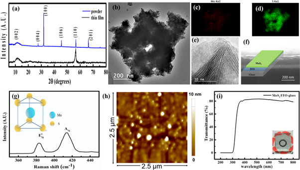
Figure 1. (a) XRD spectra of MoS2 powder and thin film, (b) TEM images of MoS2 flakes, (c) and (d) elemental mappings of the figure (b), (e) HRTEM of the MoS2 sheets, (f) cross sectional FESEM image of MoS2/ITO structure with a inset of a schematic of the same (g) Raman spectra of as-synthesized MoS2 samples, with a inset of coordination environment of MoS2 in trigonal prismatic unit cell structure (h) AFM image of the MoS2 thin layer on ITO coated glass substrate, (f) transmittance data of the MoS2 film on ITO coated glass.
Download figure:
Standard image High-resolution imageThe wavelength of the x-ray radiation used is 0.154 06 nm and assuming particles to be spherical, k, in this case, is 0.94. The average size is found to be of the order of 50 nm.
The morphology of as-synthesized MoS2 powder is further examined by transmission electron microscope (TEM). The TEM image in figure 1(b), shows the as-prepared MoS2 consists of flakes like structures and figures (c) and (d) are the corresponding elemental mapping of the MoS2. The high-resolution TEM image (figure 1(e)) depicts the two-dimensional well-resolved lattice fringes of MoS2 sample, suggesting the crystalline nature of samples, consistent with XRD results. Figure 1(f) shows the cross-sectional FESEM image of as grown MoS2 on the ITO coated glass substrate and inset represents the schematic diagram of the MoS2/ITO-glass structure. To further assess the MoS2 flakes, Raman spectroscopy was performed, as shown in figure 1(g). Two peaks arising in the curve are attributed to the in-plane vibrational  and the out-of-plane vibrational (A1g) modes, indicating the formation of MoS2 [28, 29]. Figure 1(h) displays the AFM image of the as grown MoS2 film, and the root mean square (RMS) roughness was found to be 2.426 ± 0.242 nm. Figure 1(i) shows the transmittance data of the MoS2 functional layer, with more than 80% transparency, clearly specifying the potential of the device in the transparent electronic applications.
In order to analyze the switching behavior, dc I-V characteristics of the device are observed at Room Temperature (RT). The forming voltage of the pristine Al/MoS2/ITO device is shown in figure 2(a). Initially, the device was found in the HRS. When a positive voltage was applied to the TE, the device switched from HRS to LRS at a voltage of about 4.3 V, known as the Vform [30, 31]. The forming process was carried out in the pristine device in order to initiate conduction and also to have a soft breakdown of the insulating path. In order to explore the switching uniformity, a consecutive set/reset or dc cycle process were performed after the electroforming process. Figure 2(b) shows the repetitive 100 dc cycle on Al/MoS2/ITO device, operated from +3 to −3 V, demonstrating acceptable uniformity and stability of the device performance. The multilevel cell (MLC) operation of the devices is an additional requirement for high-density data storage application. When a device has four stable and distinguishable resistance states, it can store 2 bits of information on a single device [32]. This doubles the memory density without increasing the number of memory cells integrated. The multilevel capability could be achieved by two methods [3, 7, 33]. One by current controlled scheme (CCS) which is done by controlling the current compliance (Icc) during SET processes (e.g. 10−6 A, 10−5 A, 10−4 A, 10−3 A, 10−2 A) as shown in figure 2(c). Also by voltage controlled scheme (VCS) where the stop voltage Vstop was controlled during the RESET process as shown in figure 2(d). The devices in CCS shared similar HRS. While, in CVS case, the devices had similar LRS. Different RESET stop voltages (e.g. −3.20 V, −2.80 V, −2.40 V, −2.0 V) were used to achieve multilevel HRS. In this study, we focus on the modulation of OFF state resistances by controlling the reset programming conditions, because the intermediate states between the highest and lowest states could be achieved by partially rupturing the conduction filaments. Figure 3(a) shows the cumulative distribution of the set and reset voltages for cycle-to-cycle (C/C) and device-to-device (D/D) operation. The device exhibits uniform switching during (C/C) process with the mean values (μ) for set and reset voltages as +2.17 V and −1.62 V, and also minimal standard deviation (σ) up to 7% and 10% respectively. While, during (D/D) process, the mean values (μ) of Vset and Vreset are found to be 2.20 V and −1.64 V with acceptable standard deviation (σ) of 10.5% and 14% respectively. Figure 3(a) also includes the mean value (μ) and standard deviation (σ) of the forming voltage for various devices, which are found to be 4.13 V and 27% respectively. Figure 3(b) demonstrates the cumulative probability data of the HRS/LRS for cycle to cycle and device to device operation. The mean value of the resistances (μHRS) and (μLRS) are 3.1 MΩ and 13.3 kΩ for (C/C) operation and also 3.6 MΩ and 16.7 kΩ for (D/D) operation respectively. Thus, the set/reset voltage distribution and HRS/LRS distribution without severe variation validates the uniformity and reproducibility of the proposed device. To confirm the reliability for resistive switching applications, the endurance test was performed for 104 cycles, as presented in figure 3(c). Moreover, figure 3(d) demonstrated excellent retention property of the device for 105 s. The resistances of the HRS and LRS are almost constant without much degradation.
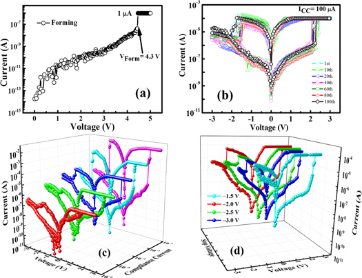
Figure 2. I–V curves of the Al/MoS2/ITO device (a) forming process, (b) bipolar current versus voltage graph upto 100th cycle, (c) demonstration of multilevel capability of the device by Current controlled scheme, (d) by Voltage controlled scheme.
Download figure:
Standard image High-resolution image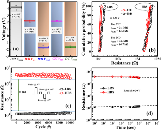
Figure 3. (a) Cumulative distribution of the set and reset voltages for cycle-to-cycle along with device-to-device operation for forming voltage also (inset), (b) cumulative probability data of the low and high resistance states, (c) endurance test, and (d) data retention property of the switching device.
Download figure:
Standard image High-resolution imageThe optical response of a device is also a key feature for the light-induced resistive switching. Figure 4(a) displays the schematic representation of the device in bias condition under visible light illumination. Figure 4(b) illustrates the bipolar switching behavior of the device under dark and light illumination. A little amount of increase in the current in HRS can be noticed and a significant decrease in set voltage (Vset) is observed in the device, when exposed to light. The increase in current may be attributed to the presence of more charge carriers inside the insulating matrix due to the generation of electron hole pair upon illumination and consequently decreases the set voltage due to the formation of conductive channel more easily [34, 35]. Whereas, during the revere bias condition, the device required additional amount of energy in terms of electric field to reset the device into HRS from LRS. Since, there was an abundance of charges due to the light exposer, forming a highly conductive and strong path may be resulting in increase in reset voltage (Vreset). Furthermore, to analyze the optical stimulation response, the device is usually biased with a fixed voltage in HRS under light illumination [36–38]. In this condition, the device can be switched to LRS from HRS by means of light pulse, due to the generation of excess charge carriers. Further, the LRS can be retained in the device upon the removal of the light source [37]. To analyze the light response behavior, in our case, the Al/MoS2/ITO device was biased with a constant voltage of +3 V in LRS under light (fixed intensity) illumination without any compliance. Figure 4(c) shows the typical photo-response curve of the device up to 14 s, where light on/off interval was maintained for 0.5 s. From the figure, it is clear that upon illumination of light, number of excitons are generated and the current rises sharply; whereas, current drops to its initial value on removal of the light. The rise time and fall time was calculated from the figure 4(d) and was found to be 0.12 s and 0.13 s respectively. The main purpose of this characterization was to check the response timing of the Al/MoS2/ITO device upon light exposer. The result shows that the device is light sensitive with fast response and can be employed to light detecting electronic devices.
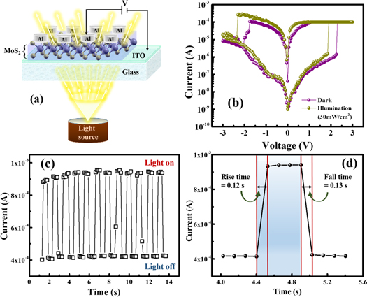
Figure 4. (a) Schematic representation of the Al/MoS2/ITO structure under visible light exposer in biased condition, (b) bipolar I–V curve of the switching device in dark and photo illumination, (c) the photocurrent response of the device, (d) enhanced view of a single photocurrent pulse.
Download figure:
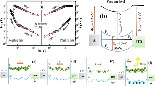
Standard image High-resolution imageIn order to know about the conduction mechanism, the I-V curves (in dark), were fitted with various existing conduction models [39, 40]. Figure 5(a) shows log-log plot of I-V for the positive and negative bias condition. Fitting data displays three distinct regions with different slopes. Under a low applied voltage, the exponential fitting parameter is about 1 for both positive and negative bias regions in HRS, indicating that electrical conduction is governed by Ohm's law, which may be due to the conduction of thermally agitated electrons. However, at higher applied voltage range, the slope is found to be ∼2 and ∼3 for positive and negative bias region respectively, and the response followed a dominant SCLC (space charge limited current) [30, 39], indicating that the mechanism may be arisen due to injection and accumulation of charge carriers through the dielectric matrix [41, 42]. However, for both the applied bias condition the slope is 1 in LRS depicting the ohmic nature and can be ascribed to the fact that a conductive filament has been formed [7, 30].
Figure 5. (a) Log-log plot of current-voltage for the positive and negative voltage sweep of the device, (b) band diagram of the Al/MoS2/ITO memory structure in non-contact mode, schematic of the charge tunneling biased at (c) +3 V, (d) −3 V (e) 0 V in dark (f) +3 V under light illumination.
Download figure:
Standard image High-resolution image
Most of the MoS2 based resistive switching mechanisms are well discussed by the electric field induced polarization of the MoS2 nano-dimensional domain [42–45]. Similarly, in the proposed Al/MoS2/ITO memory architecture, the RS mechanism can be illustrated in terms of electric field modulated polarization of the MoS2 nanodomains [42]. The effect of charge injection and accumulation inside the MoS2 assemblies play the crucial role to contribute in the switching mechanism. Figure 5(b) shows the schematic band diagram of the Al/MoS2/ITO memory structure in non-contact mode. The workfunction of Al and ITO are 4.3 and 4.8 eV respectively [39]. Despite the fact that, band gap of MoS2 (1.2 eV to 1.8 eV) rely on number of atomic layer and phase [46, 47]. The band gap and workfunction are assumed to be 1.5 eV and 4.6 eV respectively for n-type MoS2 (considering the presence of sulfur vacancies) based on the reported work [45]. When a low voltage is applied to the device very few charges start accumulating inside the MoS2 domains, making the assemblies polarized (polarization  ), after being injected from the electrode and device remains in HRS. Further increase in the applied bias results in the increase of charge density inside the MoS2 and formation of conductive pathways through the insulating layer, setting the device to LRS as shown in figure 5(c) [42]. Interestingly, the conductive channel can sustain until a specific reverse electric field is applied, which will rupture the network and set the device from LRS to HRS again as shown in figures 5(d)–(e). Moreover, taking consideration of the diffusive nature of the Al, there could be a percolation path inside the dielectric matrix governed by Al [48, 49]. As a result, this phenomenon can also be attributed to the switching mechanism of the proposed device. Further, in figure 5(f), more number of charge carriers entertains the switching mechanism due to the photo generated electron hole pair upon light illumination.
The repetitive and stable bipolar switching character, excellent endurance feature and long data retaining ability of the proposed device, introduces its implementation in the high density data storage field and the superb photo-response property of the device enhances its capability for the photodetecting application.
Conclusion
In conclusion, we can say that the work is a contributions to the systematic study on the synthesis and characteristics of the MoS2 nanostructure. The nanostructured MoS2 powder was prepared by the hydrothermal process with particle size 20–50 nm, calculated from XRD analysis. The nanocrystalline MoS2 thin film was grown on ITO coated glass substrate by simple and cost effective thermal evaporation technique. The film was found to be uniformly spread, confirmed from the surface morphology study. Current-voltage characteristic showed resistive switching with good ON/OFF current ratio and multilevel capability of Al/MoS2/ITO device. In addition, the photo-response curve showed the light sensing ability of the device with tremendous speed. Moreover, the power consumption by the device is also very less, as it can be switched to ON and OFF states at low operating voltages. At low applied voltage conduction mechanism was found to be obeying ohmic behavior, however, SCLC mechanism was observed at higher voltages.