
Abstract
The demand for high-efficiency flexible optoelectronic devices is ever-increasing because next-generation electronic devices that comprise portable or wearable electronic systems are set to play an important role. Graphene has received extensive attention as it is considered to be a promising candidate material for transparent flexible electrode platforms owing to its outstanding electrical, optical, and physical properties. Despite these properties, the inert and hydrophobic nature of graphene surfaces renders it difficult to use in optoelectronic devices. In particular, commonly used charge transporting layer (CTL) materials for organic solar cells (OSCs) cannot uniformly coat a graphene surface, which leads to such devices failing. Herein, this paper proposes an approach that will enable CTL materials to completely cover a graphene electrode; this is done with the assistance of commonly accessible polar solvents. These are successfully applied to various configurations of OSCs, with power conversion efficiencies of 8.17% for graphene electrode-based c-OSCs (OSCs with conventional structures), 8.38% for i-OSCs (OSCs with inverted structures), and 7.53% for flexible solar cells. The proposed approach is expected to bring about significant advances for efficiency enhancements in graphene-based optoelectronic devices, and it is expected that it will open up new possibilities for flexible optoelectronic systems.
Export citation and abstract BibTeX RIS
1. Introduction
Graphene, which is a 2D array of carbon atoms with a honeycomb lattice structure, is a promising candidate material for next-generation transparent conductive electrodes (TCE), and it is expected to be used as such in various optoelectronic devices owing to its superior optical, electrical, and physical properties [1–4]. More specifically, its mechanical flexibility is highly advantageous for the realization of flexible and wearable optoelectronic devices [5–7]. Currently, indium tin oxide (ITO) is one of the most widely used TCEs owing to its good optical transparency and electrical conductivity. However, its mechanical brittleness, along with its chemical instability, leads to the degradation of its physical properties and, thus, a decrease in the performance of devices that use it, which limits the number of applications it can be used in; this is especially true with regards to using it in flexible electronics.
Several synthesis routes have been developed for graphene, and they have been demonstrated to be alternatives to ITO in a wide variety of optoelectronic devices such as dye-sensitized solar cells [8–10], organic solar cells (OSCs) [11–15], perovskite solar cells [16–18], and organic light-emitting diodes [19–21]. Among this variety of synthesis approaches, chemical vapor deposition (CVD) has been demonstrated to be able to grow continuous large-area high-quality graphene films with layer controllability [22, 23], which provides desirable conditions for TCE application. CVD graphene was first demonstrated in c-OSCs (OSCs with conventional structures), and it had a power conversion efficiency (PCE) of 1.71% [11]; the potential for using CVD graphene in flexible photovoltaics applications was also demonstrated, as it had a PCE of 1.18% on polyethylene terephthalate (PET) substrates [12]. The performance of CVD graphene-based OSCs was progressively improved thereafter, with PCEs of 6.1% and 7.1% being found for conventional and inverted structures, respectively, using a low band gap polymer, poly[[4,8-bis[(2-ethylhexyl)oxy]benzo[1,2-b:4,5-b']dithiophene-2,6-diyl][3-fluoro-2-[(2-ethylhexyl)carbonyl]thieno[3,4-b]thiophenediyl]] (PTB7), and the [6,6]-phenyl-C71-butyric acid methyl ester (PC71BM) as photoactive materials [13]. Recently, Lee et al have reported on a graphene-based PTB7:PC71BM i-OSC (an OSC with an inverted structure) with a PCE of 7.51% demonstrating the solid-state n-doping of graphene by zinc oxide (ZnO) as the electron transporting layer (ETL) [15]. It has also been found that applying CVD graphene on both the top and bottom electrodes allows for the fabrication of semi-transparent OSCs, thereby avoiding the use of opaque metal electrodes [14].
The most challenging issue in using graphene as the electrode in a solution-processed OSC is the poor wettability of solution-processed charge transporting layer (CTL) materials on the surface of CVD graphene, as it is intrinsically hydrophobic in nature. It is known that such hydrophobicity originates from the stable sp2-hybridized carbon structures and relatively low surface energy of graphene, which can be further reduced from the exposure to the hydrocarbon contaminants during the transfer process of graphene [24, 25]. The resulting non-uniform coverage of CTLs on the CVD graphene electrode leads to an inevitable degradation in device performance; for example, it can lead to short-circuit currents being produced by the shunting current pathways. Several strategies for overcoming such issues have been proposed, such as the use of solvent- or surfactant-modified charge transporting materials [11, 13–15, 26], the chemical doping of graphene [20], or adding an interfacial metal oxide layer over the graphene [17]. The quality of the graphene itself is another crucial factor for achieving high-performance graphene-based OSCs; for example, chemical residues formed on graphene electrodes due to the transfer process can become impurity-induced defect sites, which can degrade the overall performance of a device [27]. The number of graphene layers also needs to be considered when balancing the electrical conductivity over the optical transmittance; increasing the number of graphene layers allows for improved electrical properties, but it sacrifices the light-harvesting capabilities of a device [28].
In this study, we propose a simple yet effective approach for improving the affinity between a graphene surface and CTLs; this approach makes use of a solvent-mediated poly(3,4-ethylenedioxythiophene)-poly(styrenesulfonate) (PEDOT:PSS) as the hole transporting layer (HTL) and ZnO-based solutions as the ETL. Using such platforms, we have developed graphene electrode-based OSCs that have outstanding PCEs of 8.38% and 7.53% on solid and flexible substrates, respectively, with high yields. These results were corroborated through various analyses focusing on the morphological and electrical characteristics of the device at the interface between the graphene electrode and the CTL.
2. Methods
2.1. Graphene electrode preparation
Graphene was synthesized on copper foil (25 µm in thickness) via low-pressure CVD method. The copper foil was loaded into the CVD chamber and annealed at 1000 °C for 30 min under hydrogen gas (10 sccm). Subsequently, methane gas was introduced at 30 sccm for 30 min for graphene growth, after which the chamber was cooled down to room temperature. Graphene sheets were then transferred onto the target substrates by poly(methyl methacrylate) (PMMA)-assisted transfer method and the supporting PMMA layer was finally removed by acetone [29]. The transfer process was repeated to obtain four-layer stacked graphene electrodes.
2.2. Solar cell fabrication
ITO/glass substrates were cleaned by sonication in soap water, DI water, acetone, and isopropanol, followed by oxygen plasma treatment. Graphene/glass substrates were rinsed by acetone and isopropanol. Solvent-mediated PEDOT:PSS solutions were spin-coated on ITO or graphene at 4000 rpm for 1 min, followed by annealing at 110 °C for 10 min in ambient air. ZnO solutions were spin-coated at 3000 rpm for 1 min, followed by annealing at 175 °C for 10 min. PTB7, PTB7-Th, and PC71BM were dissolved in a mixed solvent of chlorobenzene:1,8-diiodooctane (97:3 vol%) at concentrations of 12, 12, and 40 mg ml−1, respectively. The blended solutions of PTB7:PC71BM (2:1 vol%) and PTB7-Th:PC71BM (2:1 vol%) were spin-coated at 900 rpm for 2 min under nitrogen environment. MoO3, Al, and Ag were thermally evaporated under high-vacuum conditions at base pressure of 8 × 10⁻⁷ Torr.
2.3. Measurements and characterization
J–V characteristics of solar cells were measured using Xenon arc lamp (300 W) solar simulator and keithley 2635 A source measurement unit in a nitrogen-filled glovebox. Shadow mask was used during the measurement to prevent any potential overestimation over the actual device area. Light intensity dependence of Jsc and Voc was measured using neutral density filters. EQE measurements were performed using the QE system (QEX7, PV measurements) under ambient conditions. The surface morphology analysis was performed using dimension AFM (DI-3100, Veeco) operated in tapping mode, SEM (S-4800, Hitach), and OM (Eclipse LV150, Nikon). UPS measurements were conducted using He I (21.2 eV) discharge lamp (ESCALAB 250Xi, Thermo Fisher Scientific) under ultra-high vacuum condition (<10−10 Torr).
3. Results and discussion
When using CVD graphene as a transparent conductor in OSCs, the role of selective CTLs becomes critical due to both graphene's inert nature and its work function, which is lower than that of ITO. While the surface properties and energy levels of ITO can be readily modified (for instance via simple plasma treatments) without sacrificing its optical or electrical properties, such approaches are not readily applicable for CVD graphene [30]. Figure 1(a) illustrates an example of the energy level tuning of both graphene and ITO [31, 32]. Although the work function of graphene can be tuned with the number of layer (from 4.4 eV for monolayer to 4.7 eV for four-layer graphene), its effect is relatively small compared to plasma-treated ITOs. The work function of pristine as-sputtered ITO (4.7 eV) can be simply modulated from the O2 plasma treatment (5.2 eV). Moreover, the hydrophobic nature of graphene surfaces cannot be modified unless the sp2-hybridized carbon structures are significantly disrupted, which would lead to the degradation of graphene's electrical property (figure 1(b)). In organic photovoltaics, a variety of CTL materials such as PEDOT:PSS, TiOx, and ZnO are used due to them having appropriate energy level alignments at the electrode and photoactive layer interface [33, 34]. As for HTL materials, aqueous solution-based PEDOT:PSS is the most widely used, even beyond the OSC application, which, however, is difficult to coat on a graphene surface. To enhance the wettability of PEDOT:PSS on graphene, we investigated how two alcohol solvents, namely methanol (MeOH) and isopropanol (IPA), acted as the PEDOT:PSS modifier (henceforth they are referred to as m-PEDOT:PSS and i-PEDOT:PSS, respectively). The use of a PEDOT:PSS solution mixed with IPA as a HTL in a graphene electrode-based c-OSC has previously been reported upon, and it was demonstrated to have improved wettability on the hydrophobic surface of graphene [13, 35]. In these studies, an additional MoO3 electron blocking layer was included so as to improve charge selectivity and avoid carrier recombination at the interface between the PEDOT:PSS and photoactive layers; this was done to prevent the PEDOT:PSS-only devices performing unstably when using the graphene TCE, especially with regards to the device yield. However, the MoO3 layer was shown to be vulnerable to the choice of processing solvents used for the photoactive materials; thus, additional treatments were needed to avoid the device performance from degrading. The additional MoO3 layer was also found to reduce the amount of light absorbed and increase the interfacial bulk series resistance of the completed solar cells due to its insulating nature. Our investigation reveals that when m-PEDOT:PSS HTL is used with graphene, it helps mitigate the low device yield observed from i-PEDOT:PSS-based devices without needing to use any additional MoO3 charge selective layers.

Figure 1. Morphological and Electrical analysis of solvent-mediated PEDOT:PSS in the application of graphene. (a) Work function change of graphene in terms of the number of layer and that of ITO upon O2 plasma treatment. (b) Effect of O2 plasma treatment to graphene. Shown in the inset is the contact angle change of water on graphene surface. (c) Contact angle measurements of PEDOT:PSS, m-PEDOT:PSS, and i-PEDOT:PSS solutions on graphene. (d) Sheet resistance and optical transmittance of PEDOT:PSS, m-PEDOT:PSS, and i-PEDOT:PSS films spin-coated on SiO2 and glass substrates. The average values of sheet resistance are presented with error bars. (e) Cut-off and (f) onset region of UPS spectra of pristine graphene (4.4 eV, black line) and graphene covered by m-PEDOT:PSS (5.2 eV, red line) or i-PEDOT:PSS (5.0 eV, blue line) solutions.
Download figure:
Standard image High-resolution imageTo examine the wetting properties of solvent-mediated PEDOT:PSS solutions, we performed contact angle measurements. Figure 1(c) shows the contact angle images of PEDOT:PSS, m-PEDOT:PSS, and i-PEDOT:PSS on graphene; from it, we can see that the m-PEDOT:PSS and i-PEDOT:PSS had much better wettability than the pristine PEDOT:PSS with contact angles of 82°, 58°, and 46°, respectively, owing to the reduced surface energy of the overall solution [36]. In addition to the enhanced wettability, another beneficial effect from adding the solvent to the PEDOT:PSS is that it improves the electrical conductivity of the PEDOT:PSS film. As shown in figure 1(d), both the m-PEDOT:PSS and i-PEDOT:PSS films had much lower sheet resistance than the pristine PEDOT:PSS, with the three obtaining values of 1.65, 2.03, and 11.86 MΩ sq−1, respectively. Organic solvents like MeOH are known to induce a screening effect between the PEDOT and PSS components and can help remove the insulating PSS shell from the PEDOT core, which leads to an improvement in the overall conductivity of PEDOT:PSS materials [37]. Such enhanced electrical conductivity in HTLs can lower the interfacial contact resistance, which then promotes a more efficient charge transfer at the photoactive layer and electrode interface. Transmittance measurements were also performed to investigate the optical properties of solvent-mediated PEDOT:PSS solutions. As shown in figure 1(d), additional solvents did not have any noticeable effect on the optical transmittance of PEDOT:PSS, which had similar transmittance values in different configurations of the PEDOT:PSS. The results in figure 1(d) are summarized in table S1 (stacks.iop.org/TDM/4/045004/mmedia).
The effect of the solvent treatment on the electrical properties of the PEDOT:PSS was further investigated using ultraviolet photoemission spectroscopy measurements; these were used to determine the change in the work function of graphene when it was covered by the m-PEDOT:PSS and i-PEDOT:PSS solutions. As shown in figures 1(e) and (f), the work function of the pristine graphene was found to be approximately 4.4 eV, consistent with previously reported values [31], which increased to 5.2 and 5.0 eV after coating the m-PEDOT:PSS and i-PEDOT:PSS, respectively. A uniform coverage of the PEDOT:PSS layers is expected to facilitate hole extraction from the photoactive layer to the graphene electrode by minimizing the energy barrier induced by the difference between the work function of graphene and the highest occupied molecular orbital of the donor material. The slightly higher work function of m-PEDOT:PSS over i-PEDOT:PSS also suggests that the former may elicit a more efficient hole extraction.
For the thin layered OSC structures, which are typically less than a few hundred nanometers thick, the uniformity of the surface morphology in each layer plays an important role in determining the overall device performance since non-uniform layers with pin-holes can act as potential defect sites for shunting pathways [38]. Figure 2 demonstrates the effect of additional solvents on the thin film formation of PEDOT:PSS on the surface of graphene, which we investigated using optical microscopy (OM) and atomic force microscopy (AFM). Corresponding scanning electron microscopy images are shown in figure S1. Unlike the solvent-mediated PEDOT:PSS, the non-wettability of aqueous PEDOT:PSS on graphene can be readily confirmed from the OM images in figures 2(a)–(c). Water-based PEDOT:PSS is difficult to coat on the hydrophobic surface because the high surface tension of water (71.7 dyne cm−1) [39] typically results in the large cohesive force in PEDOT:PSS compared to the adhesive force between the PEDOT:PSS and graphene surface. Addition of IPA or MeOH, with their lower surface tensions than water (20.8 and 22.4 dyne cm−1, respectively), into PEDOT:PSS, can reduce the cohesive force in PEDOT:PSS. Therefore, the increased adhesive force between the modified PEDOT:PSS and graphene surface significantly enhanced the conformal coverage of the PEDOT:PSS thin film over the graphene surface [40]; this can be further corroborated using the AFM images in figures 2(d)–(g). The AFM images also revealed the good uniformity of the solvent-mediated PEDOT:PSS thin films on graphene, which shows similar surface morphology profile to the reference ITO/PEDOT:PSS; root-mean-square roughness values of 0.94, 0.90, 0.98, and 0.92 nm were obtained for the PEDOT:PSS on ITO, m-PEDOT:PSS and i-PEDOT:PSS on graphene, and graphene, respectively.
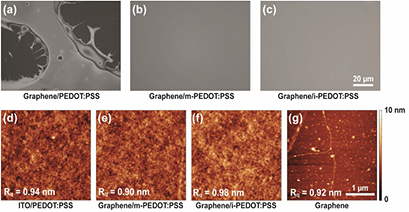
Figure 2. Surface morphology of different configurations of PEDOT:PSS on graphene transferred on SiO2 substrates. OM images of (a) PEDOT:PSS, (b) m-PEDOT:PSS, and (c) i-PEDOT:PSS solutions on graphene. AFM images of (d) PEDOT:PSS on ITO, (e) m-PEDOT:PSS and (f) i-PEDOT:PSS on graphene, and (g) graphene. AFM image of (g) graphene is shown for the reference.
Download figure:
Standard image High-resolution imageAfter obtaining the conformal PEDOT:PSS HTL on graphene, the graphene/PEDOT:PSS stack was then applied to c-OSCs using poly[4,8-bis(5-(2-ethylhexyl)thiophen-2-yl)benzo[1,2-b;4,5-b']dithiophene-2,6-diyl-alt-(4-(2-ethylhexyl)-3-fluorothieno[3,4-b]thiophene-)-2-carboxylate-2-6-diyl)] (PTB7-Th) and PC71BM as the donor and acceptor photoactive materials [41–44], respectively, to create high-performance graphene-based devices. An Al cathode (100 nm) was thermally evaporated onto the photoactive layer so as to complete the device. Four layer of stacked CVD graphene was used as the TCE, which was prepared using the wet transfer method; it had an average sheet resistance and transmittance of 286 ± 12 Ω sq−1 and 90.3% at 550 nm, respectively.
The schematic structure and corresponding flat-band energy level diagram of the graphene-based devices are shown in figures 3(a) and (b). Figure 3(c), meanwhile, shows the current density–voltage (J–V) characteristics of the graphene electrode-based OSCs along with the reference ITO device as measured under simulated AM 1.5 G illumination at 100 mW cm−2 irradiance. The corresponding key photovoltaic parameters are summarized in table 1. The optimized graphene-based PTB7-Th:PC71BM champion device with the m-PEDOT:PSS had a PCE of 8.17% with a short-circuit current (Jsc) of 16.96 mA cm−2, an open-circuit voltage (Voc) of 0.79 V, and a fill factor of 61.2%, reaching close to 90% of the performance of the ITO-based reference device (PCE = 9.24%). The graphene device with the i-PEDOT:PSS had a slightly lower performance, with a PCE of 8.11%. As expected, there was a negligible difference in the device performance for the ITO case when solvent-mediated PEDOT:PSS HTLs were used (see figure S2 and table S2). This result is one of the highest efficiencies ever reported for graphene electrode-based c-OSCs. The slightly lower Jsc of the graphene-based devices than for the ITO-reference devices, originating from the lower conductivity of the graphene electrode, are also reflected in the external quantum efficiency (EQE) measurements shown in figure 3(d). The ITO-based devices had a higher EQE in the range of 410–800 nm, but a lower EQE below the 410 nm region than the graphene-based devices did; below the 410 nm, the transmittance of ITO decreases rapidly, while graphene maintains a uniformly high transmittance across the entire spectrum of 300–800 nm [4]. We note that the overall performance of the m-PEDOT:PSS-based devices was better than that of the i-PEDOT:PSS devices, as they had a higher average PCE and a narrower distribution in their device performance, which led to a better device yield, as shown in figure 3(e) and table 1.
Table 1. Device performance parameters of ITO/PEDOT:PSS, graphene/m-PEDOT:PSS, and graphene/i-PEDOT:PSS-based PTB7-Th:PC71BM c-OSCs.
| Anode | HTL | Jsc (mA cm−2) | Voc (V) | FF (%) | PCE (%) |
|---|---|---|---|---|---|
| ITO | PEDOT:PSS | 17.66 (17.60 ± 0.06) | 0.799 (0.793 ± 0.006) | 65.5 (64.6 ± 0.9) | 9.24 (9.02 ± 0.22) |
| Graphene | m-PEDOT:PSS | 16.96 (16.72 ± 0.24) | 0.787 (0.770 ± 0.017) | 61.2 (59.8 ± 1.4) | 8.17 (7.66 ± 0.51) |
| Graphene | i-PEDOT:PSS | 16.65 (16.32 ± 0.33) | 0.770 (0.744 ± 0.026) | 62.8 (56.6 ± 6.2) | 8.11 (6.86 ± 1.25) |

Figure 3. Device performance of graphene-based OSCs in conventional structure with ITO-reference: anode (graphene or ITO)/HTL/PTB7-Th:PC71BM/Al. (a) Schematic of conventional device and (b) its corresponding flat-band energy level diagram. (c) J–V characteristics and (d) EQE measurements of ITO (black line), graphene/m-PEDOT:PSS (red line), and graphene/i-PEDOT:PSS (blue line) devices. (e) Distribution of solar cell performance for graphene-based devices.
Download figure:
Standard image High-resolution imageTo investigate the charge recombination kinetics of the completed solar cells, the light intensity (I) dependence of the J–V characteristics was further analyzed. In general, Jsc follows a power-law dependence on light intensity, as  , where
  is a power-law scaling exponent [45, 46]. As shown in figure 4(a), the linear dependence of Jsc with
  indicates that dissociated charges after photoexcitation at the bulk-heterojunction interface of the photoactive layers are effectively extracted to each electrode without nongeminate recombination in both the ITO- and graphene/m-PEDOT:PSS-based devices. However, the graphene/i-PEDOT:PSS-based devices with the dependence of Jsc with
  indicates that free charge carriers were lost due to the nongeminate recombination that occurred at the interface between the i-PEDOT:PSS and the photoactive layer; this can be attributed to the slightly higher sheet resistance of i-PEDOT:PSS than m-PEDOT:PSS films, as previously mentioned in this section.

Figure 4. Light intensity dependence of (a) Jsc and (b) Voc of ITO- and graphene-based OSCs in conventional structure. Graphene/m-PEDOT:PSS device shows slightly better recombination kinetics than the i-PEDOT:PSS case. Solid lines indicate linear fitting of each measurement points.
Download figure:
Standard image High-resolution imageUnder open-circuit conditions, all of the photogenerated charge carriers recombine, which results in zero extraction current. Detailed information about the associated recombination dynamics can be obtained via the light intensity dependence of Voc as  , where n, k, T, and q are the ideality factor, Boltzmann constant, temperature, and elementary charge, respectively. In several organic bulk-heterojunction solar cells, the recombination kinetics are largely influenced by the trap-assisted recombination, which can be inferred from the slope of Voc versus
  [47]. Figure 4(b) shows that both the ITO- and graphene-based devices are affected by the trap-assisted recombination process to similar degrees. These results suggest that the main difference between the device performance of the ITO- and graphene-based OSCs is due to the quality of the CVD graphene, which can potentially be degraded by the transfer process [29] as well as the general lower electrical conductivity of graphene as compared to ITO [28]. The above light intensity measurements revealed that the overall charge recombination kinetics were more favorable for the graphene/m-PEDOT:PSS devices than for the i-PEDOT:PSS ones, which was consistent with the device performance results that can be observed in figures 3(c)–(e).
To demonstrate the processing compatibility of m-PEDOT:PSS and i-PEDOT:PSS with other photoactive materials, the solvent-mediated HTLs were used in graphene-based PTB7:PC71BM c-OSCs with the following structures: ITO or graphene/HTL/PTB7:PC71BM/Al (100 nm). The corresponding J–V characteristics and EQE results are shown in figure S3. The m-PEDOT:PSS-based graphene device had a PCE of 7.42%, which was approximately 94% of the ITO-based reference device (PCE of 7.91%). The i-PEDOT:PSS-based graphene device also performed well, with a PCE of 7.12%. The related photovoltaic parameters are summarized in table S3. These results confirm the adaptability of the proposed approach in general OSC applications.
To validate the versatility of the proposed solvent-mediated modification in CTLs, such an approach was investigated further in i-OSC configurations. Inverted device structures avoid using both acidic PEDOT:PSS and easily oxidized low work function metal electrodes, which can be detrimental to the long-term operation of a device, especially in ambient air conditions [34, 48]. In i-OSCs, solution-processed TiOx or ZnO are usually used as the ETL, but as before, it is difficult to coat the graphene surface with these materials and achieve good uniformity. For instance, as shown in figure S4, a typical ZnO sol-gel solution, namely zinc acetate dihydrate (ZAD) dissolved in 2-methoxyethanol and ethanolamine, cannot be uniformly coated on graphene. However, ZAD dissolved in MeOH has found to have good wettability on graphene and provide uniform coverage. We also explored the potential for flexible devices, and the final device structures were as follows: glass or PET/ITO or graphene/ZnO/PTB7-Th:PC71BM/MoO3 (20 nm)/Ag (100 nm), as shown in figures 5(a) and (b). The associated J–V characteristics and corresponding EQE measurements are shown in figures 5(c) and (d).

Figure 5. Device performance of graphene-based OSCs in inverted structure with ITO-reference: cathode (graphene or ITO)/ZnO/PTB7-Th:PC71BM/MoO3/Ag. (a) Schematic of inverted device and (b) its corresponding flat-band energy level diagram. (c) J–V characteristics and (d) EQE measurements of ITO (black line) and graphene (red line) device on glass substrates, and the graphene device on flexible PET substrate (blue line). The inset in (c) shows the digital image of graphene-based flexible device.
Download figure:
Standard image High-resolution image
The graphene-based i-OSC managed to obtain notably high PCEs of 8.38% and 7.53% on the glass and flexible PET substrates, respectively. These results are summarized in table 2. To the best of our knowledge, these results are one of the highest efficiencies reported for graphene-based OSCs, both on solid and flexible substrates; this demonstrates the potential for creating high-performance graphene-based flexible OSCs.
Table 2. Device performance parameters of ITO and graphene-based PTB7-Th:PC71BM i-OSCs on glass and PET substrates.
| Substrate | Cathode | Jsc (mA cm−2) | Voc (V) | FF (%) | PCE (%) |
|---|---|---|---|---|---|
| Glass | ITO | 17.12 (17.03 ± 0.09) | 0.788 (0.786 ± 0.002) | 68.1 (67.8 ± 0.3) | 9.22 (9.08 ± 0.14) |
| Glass | Graphene | 16.50 (16.42 ± 0.08) | 0.773 (0.768 ± 0.005) | 65.6 (64.4 ± 1.2) | 8.38 (8.12 ± 0.26) |
| PET | Graphene | 16.01 (15.75 ± 0.26) | 0.757 (0.734 ± 0.023) | 62.0 (58.3 ± 3.7) | 7.53 (6.74 ± 0.79) |
4. Conclusions
In this study, commonly used CTLs, both the electron and HTLs, were successfully implemented into graphene electrodes using a facile solvent-mediated approach. We then demonstrated that they could be used to fabricate high-performance graphene-based OSCs, both in conventional and inverted configurations. Without using any additional electron blocking layers (i.e. only in the presence of a solvent-mediated PEDOT:PSS HTL), we were able to obtain a high PCE of 8.17% along with a high device yield for the graphene-based c-OSCs. With appropriate integration of a ZnO ETL on the graphene electrodes, the graphene-based i-OSCs achieved a notably high PCE of 8.38%, which is one of the highest efficiencies ever reported for single-junction graphene electrode-based OSCs. The functionality of the graphene-based devices utilizing the solvent-mediated CTLs was corroborated through several morphological and electrical analyses, including interfacial charge transfers and the recombination dynamics in the completed device. The high performance of the graphene-based OSCs on flexible substrates (PCE = 7.53%) also suggests that these graphene electrode could potentially be used for portable or wearable devices. Overall, the advances in graphene electrode-based solar cells demonstrated by this study are expected to facilitate the application of graphene in various optoelectronic devices so that are used in many more devices than just in solar cells.
Acknowledgments
This work was supported by Basic Science Research Program through the National Research Foundation of Korea (NRF) funded by the Ministry of Science, ICT & Future Planning (2015R1D1A1A0105791) and National Research Foundation of Korea (NRF) grant funded by the Korea government (MSIP) (2015R1A2A1A10053397). This work was also supported by the Free Innovative Research Fund (1.170003.01) of UNIST (Ulsan National Institute of Science and Technology).