
Abstract
Two-dimensional (2D) transition metal dichalcogenides (TMDs), like MoS2, have unique electronic and optical properties, which can further be tuned using ion bombardment and post-synthesis ion-beam mediated methods combined with exposure of the irradiated sample to precursor gases. The optimization of these techniques requires a complete understanding of the response of 2D TMDs to ion irradiation, which is affected by the reduced dimensionality of the system. By combining analytical potential molecular dynamics with first-principles calculations, we study the production of defects in free-standing MoS2 sheets under noble gas ion irradiation for a wide range of ion energies when nuclear stopping dominates, and assess the probabilities for different defects to appear. We show that depending on the incident angle, ion type and energy, sulfur atoms can be sputtered away predominantly from the top or bottom layers, creating unique opportunities for engineering mixed MoSX compounds where X are chemical elements from group V or VII. We study the electronic structure of such systems, demonstrate that they can be metals, and finally discuss how metal/semiconductor/metal junctions, which exhibit negative differential resistance, can be designed using focused ion beams combined with the exposure of the system to fluorine.
Export citation and abstract BibTeX RIS

Original content from this work may be used under the terms of the Creative Commons Attribution 3.0 licence. Any further distribution of this work must maintain attribution to the author(s) and the title of the work, journal citation and DOI.
1. Introduction
Beams of energetic ions and electrons are powerful tools to change the morphology and properties of both bulk [1, 2] and nano [3–5] materials. This is particularly relevant to two-dimensional (2D) systems, as their 'thickness' is smaller than the ranges of even low-energy particles, so that the whole structure can easily be treated, as opposed to macroscopically large objects where much higher energies of electrons and especially ions are required, and the effects of irradiation on sample morphology are spatially nonuniform.
The very nature of 2D materials, which consist of only surface, also opens new routes for ion and electron beam engineering of their structure and properties through controllable introduction of defects [6]. In addition to 'direct' methods of nanomaterial processing such as cutting the target by atom sputtering [7–13], changing its stoichiometry [14, 15], welding system parts [16, 17] by creating reactive defects at their surfaces, or impurity atom implantation [18–20], beam-mediated techniques can be used when irradiation is combined with exposure to precursor gases, similar to bulk systems [21]. For instance, atoms can be sputtered away from a 2D material, followed by an exposure to chemical species which fill the vacancies, so that impurities can be introduced into the system with a high spatial resolution if focused beams are used. The precursor gas can also be added during the irradiation, and the beam will break gas molecules thus providing reactive species. Examples of post-synthesis beam-mediated treatments of 2D materials include doping of hexagonal boron nitride with carbon [22], or graphene with metal atoms [23].
Experiments [24–26] and simulations [27, 28] indicate that the response of 2D targets to irradiation is different in many ways from that of bulk materials. Deposition of the energy by the energetic particle and its redistribution can also be different in systems with reduced dimensionalities [4], which may affect defect production, and thus justifies investigations of irradiation-induced phenomena in 2D targets.
So far, most of the ion irradiation studies on 2D materials have been done for graphene, a monoatomic solid, and much less is known about the response of other 2D systems to ion beams. Specifically, the behavior of 2D transition metal dichalcogenides (TMDs), which are composed of atoms of several types, under ion irradiation has not been studied systematically. At the same time, these materials are of particular interest, since they have already shown appealing potential for nanoelectronics, photonics, catalysis, and energy applications due to a unique combination of electronic, optical, and mechanical properties [29–32]. New functionalities can also be added to 2D TMDs by using irradiation directly or by attaching molecules and atoms to vacancies. Indeed, first experiments [33] showed that the transport characteristics of a MoS2-monolayer (ML) field effect transistor can be modulated via irradiation with swift heavy ions. A similar technique has been used for defect engineering in single- and few-layer of MoS2 [34]. The experimental results on the bombardment of MoSe2 and WSe2 MLs using a helium ion microscope indicated that the ion beam changes the electronic structure, shifts optical response towards the visible region and even increases the elastic Young's modulus [35, 36]. The presence of magnetic ordering in proton-irradiated bulk MoS2 samples was recently reported [37] indicating that spin-polarized transport and magnetism can be realized in 2D TMDs. Furthermore, the possibility of selective desulfurization of MoS2-ML through a low-energy argon ion irradiation [38] and the post-growth tuning of band gap in MoS2-ML by substitution of top-layer sulfur atoms with selenium atoms [39] has been demonstrated. It has also been shown that the stoichiometry of few-layer MoS2 flakes can be changed by He ion irradiation, and ribbons about 9 nm wide can be produced [40].
To fully leverage the opportunity of irradiation treatment of 2D TMDs, it is imperative to understand the response of these materials to impacts of energetic particles and find optimum parameters, such as particle energies, angles, ion mass, etc for efficient atomic structure engineering using ion bombardment. To this end, atomistic computer simulations are an indispensable tool for getting microscopic insights into defect production mechanisms in solids under irradiation [41]. At the same time, while the behavior of MoS2, the most wide-spread member of the TMD family, under electron beam has been addressed [42], there is no theoretical data on the production of defects in these systems under ion irradiation.
Here, we assess the effects of ion irradiation on suspended MoS2-ML by using analytical potential molecular dynamics (MD) simulations combined with density-functional theory (DFT) methods. We characterize the types and assess the abundance of point defects which appear in MoS2 under irradiation with various noble-gas ions in a wide range of ion energies. We demonstrate that the ratio of the atoms sputtered from upper and bottom sulfur layers can be tuned by choosing the appropriate energy and incident angle of the ion beam. Finally, we show the possibility for engineering mixed MoSX compounds where X are chemical elements from group V or VII, and discuss the properties of such systems and lateral MoSX-MoS2 heterostructures.
2. Methods
2.1. Molecular dynamic simulations of ion irradiation
The LAMMPS package [43] is used to perform all classical simulations. A 2D periodic boundary condition is applied parallel to the basal plane of MoS2. All structures are fully optimized using a nonlinear conjugate gradient energy minimization method available in LAMMPS. The interaction between ions (noble gas) and MoS2-ML was constructed by the Ziegler–Biersack–Littmark (ZBL) universal repulsive potential [44] for modeling energetic collisions, which can accurately describe the interaction between atoms at small separations (<1  ). We have used an adaptive time step for impact simulations as implemented in LAMMPS. Using this method, the time step is defined depending on the velocity of fastest moving atoms in the system, varying from almost one attosecond to one femtosecond. The ion irradiation simulations were carried out using a MoS2 supercell containing 1254 atoms. This supercell corresponds to the
  unit cells of the ideal lattice with dimensions of about
 2 in a rectangular representation (figure 1(a)). As strain is known to affect the response of nanomaterials to irradiation [45, 46], the supercell size was carefully optimized. The impact points for ion irradiation were randomly/uniformly selected within the minimum irreducible area of the lattice (figures 1(b) and S1). Our benchmark calculations for both uniform and random impact distribution showed that a minimum of 150 impact points can give very similar statistics from MD simulations (see figure S1). In order to adequately model the distribution of the energy brought in by the ion into the system and the evolution of the atomic structure after the impact, the system was quenched to zero temperature during a time period of 10 ps using a Nosé–Hoover thermostat. We performed 4896 independent simulations for each ion and angle that resulted in a total number of
  150 000 simulations.

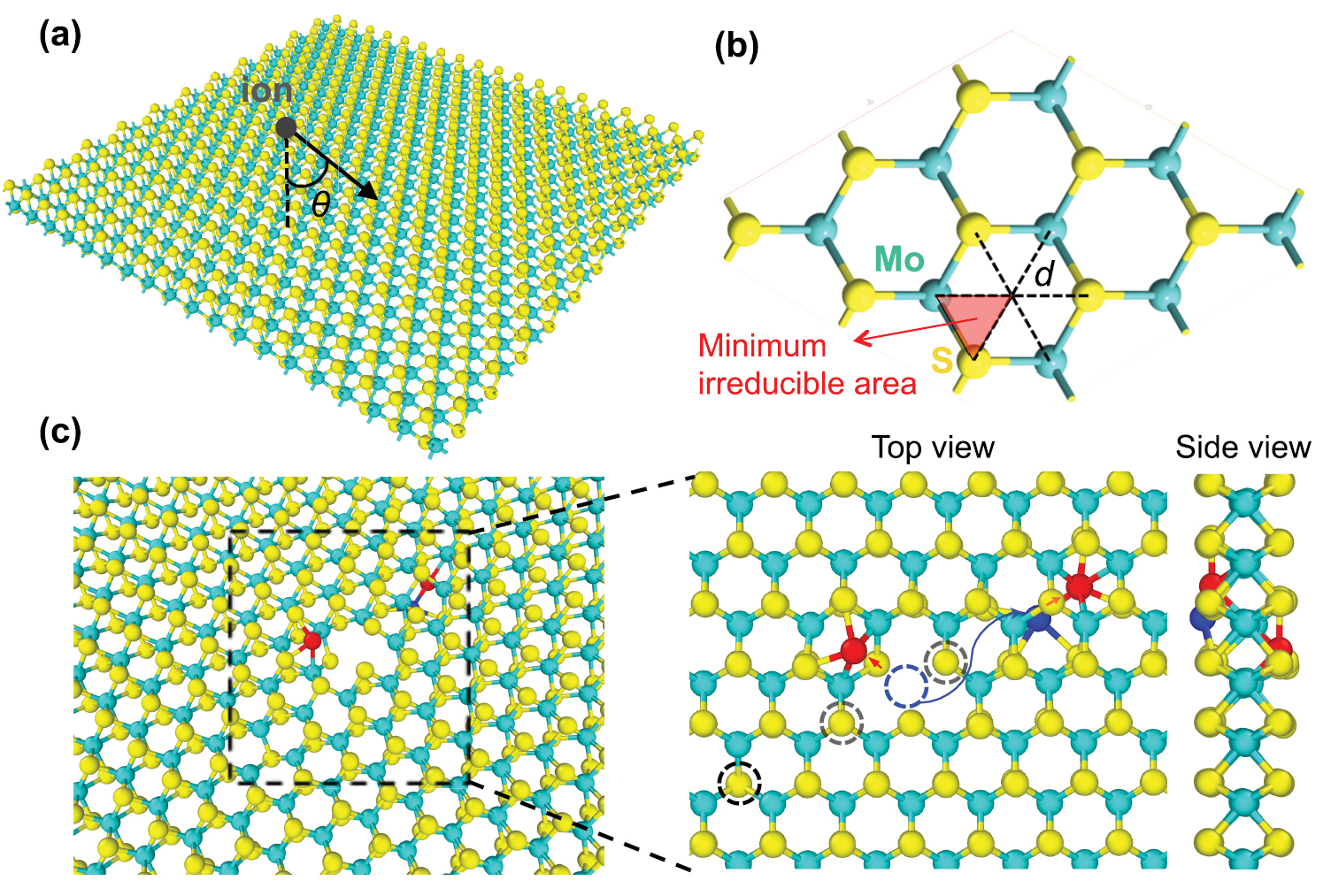
Figure 1. (a) Schematic illustration of the setup for ion irradiation simulations of MoS2-ML. Molybdenum and sulfur atoms are shown in blue and yellow, respectively. (b) Definition of the minimum irreducible area (the red triangle) used for ion impacts. (c) A typical atomic structure of the target after an impact of an Ar ion with an energy of 254 eV and normal incidence ( ). Black dashed circles represent single S vacancies, the blue dashed circle shows a Mo vacancy and red atoms display S atoms with trigonal symmetry configuration, as in the T phase.
Download figure:
Standard image High-resolution image2.2. Electronic structure and transport calculations
Density-functional theory (DFT) calculations with the PBE [47] exchange-correlation functional have been carried out using the Atomistix ToolKit (ATK) code [48]. An SCF convergence tolerance of 0.0001 Hartree and a kinetic energy cutoff of 150 Hartree have been used for the calculations. A vacuum space of 30  was set normal to the layer for avoiding any artificial interaction between the layer and its periodic images. The Brillouin zone (BZ) of the unit cell system and the transport model were sampled using
  and
and  k points, respectively. The electron transport calculations were performed using the DFT method in conjunction with the non-equilibrium Green's function (NEGF) [49] approach as implemented in ATK. Poisson equation was solved using a fast Fourier transform solver in a self-consistent manner. The NEGF method has already been applied to study electron transport in various TMDs [50, 51].
3. Results and discussion
In order to get microscopic insights into defect production under ion impacts in free-standing MoS2-ML, we carried out MD simulations as described in the Methods section. We considered the limit of low energies of ions when nuclear stopping dominates over electronic stopping. The simulation setup is shown in figure 1, which also presents the minimum irreducible area (the red triangle) used in ion impact simulations. We addressed low-dose irradiation, so that it was assumed that there is no cumulative effect originating from impacts of several ions into the same area.
We first assessed the ability of the interatomic potentials available for MoS2-ML to describe atomic structure and energetics of point defects. We systematically calculated formation energies for different point defects using four available potentials [52–56] for MoS2-ML and compared those to the energies obtained using DFT calculations [57]. These results are shown in figure 2. We analyzed 8 types of point defects, with most of them being observed in transmission electron microscopy (TEM) experiments [6, 42, 58, 59].
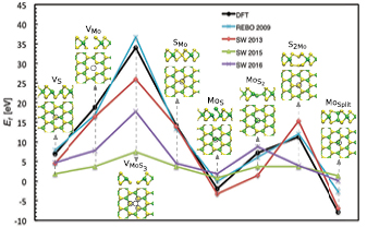
Figure 2. Comparison between formation energies of various type of defects calculated using DFT and empirical potentials. Different types of defects in MoS2-ML, from left: vacancies (I)–(III), antisites (IV)–(VII), and the Mo–Mo split interstitial (VIII). Black dashed circles show the position of the defect.
Download figure:
Standard image High-resolution imageThe formation energies of defects were calculated as:  , where Ebulk and Edef are the energies of the pristine system and defect containing supercell.
  represents the chemical potential of the X species, which is taken as the energy of the isolated atom (group). Such a choice of the chemical potentials is the most adequate for the physical problem we consider. By default
  in analytical potential calculations for all isolated atoms, and the DFT values are also close to zero,
  eV.
eV.
Among the considered potentials, the many-body reactive empirical bond-order (REBO) [52] and Stillinger–Weber (SW) 2013 potential [54] provide the best agreement in comparison to the DFT results [57]. The formation energy of single S vacancies as obtained from REBO in our calculations also agrees with the previously reported values [60], while the SW 2013 potential underestimates it by some 20% giving rise to a shift in ion threshold energies for defect production, as discussed below. As another important test, we also calculated the difference in energy between the 1T and 2H phases of MoS2. The SW 2013 potential gives a better description of the phases, while REBO underestimates the energy difference (table S1). Another feature of the SW potential is that it is computationally efficient, being faster than REBO by a factor of 12. Based on the above, we conducted most of the calculations using the SW 2013 potential and verified some of the results using REBO. Using molecular dynamic simulations, we also calculated the displacement threshold energies (Td
) for Mo and S, i.e. the minimum kinetic energy required to transfer to S/Mo atom in order leave its position in the system in a binary collision. The displacement thresholds for the SW potential were found to be  eV and
  eV for sulfur and molybdenum, respectively. The results are in line with the energies previously obtained using DFT [42], as shown in table S2.
Figure 3 presents the average number of sputtered target atoms as a function of ion energy ranging from 10 eV to 1000 keV. Mostly S vacancies are produced, including single and double vacancies with two missing S atoms on top of each other. This is consistent with the results of early experimental studies of MoS2 surfaces subjected to ion irradiation [61, 62]. S adatoms and S atoms displaced from the H to the distorted T positions shown in red in figure 1(c) were also rather common, but our MD simulations indicated that these defects should not be stable on macroscopic time scales even at room temperature.
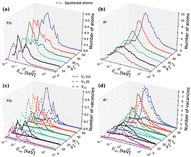
Figure 3. Upper panels: average numbers of sputtered atoms in MoS2-ML as functions of ion energy and incident angle for He (a) and Ar (b) ions. Lower panels: the corresponding numbers of S vacancies produced in the upper layer (VS (u)), the lower layer (VS (l)) and Mo vacancies (VMo) for He (c) and Ar (d).
Download figure:
Standard image High-resolution imageSputtering yield initially grows with ion energy up to a maximum value and then decreases, contrary to bulk targets where the total amount of damage is proportional to particle energy. The drop in the number of defects (average number of defects per ion impact) produced in 2D systems at high energies is due to the absence of collisional cascades in atomically thin targets, as shown for graphene [27] and h-BN [63], and a smaller cross section for energy transfer from the ion to the recoil atom at high ion energies[4]. The number of defects created in MoS2-ML due to ion impacts also follows this trend. The data for other ions (Ne, Kr, and Xe) is shown in figure S2. It can be seen that the minimum ion energy for defect production (Emin) depends on ion mass. This should be immediately clear from the kinematic factor describing a head-on binary collision  , where Td
is the S atom displacement energy, and mi
(mt
) represent ion (target atom) masses.
, where Td
is the S atom displacement energy, and mi
(mt
) represent ion (target atom) masses.
The results presented in figures 3 and S2 indicate that the incident angle (θ) has a significant effect on defect production. In general, the number of sputtered atoms increases with θ. The peak in the sputtering yield versus ion energy curve shifts towards higher energies with tilting the ion beam direction from normal, as larger incident angles increase the projected atomic density of the target in the ion direction.
In order to better characterize defect production in MoS2-ML under ion irradiation, single vacancies produced by ion impacts were divided into 3 main categories: S vacancy in the upper layer, Mo vacancy and S vacancy in the lower layer. As evident from figures 3 and S2, the probability for S vacancies to appear is significantly higher than that for Mo vacancies due to much higher threshold displacement for Mo than S. As for S vacancies, the ratio of the defect numbers in the upper and bottom layers depends on ion energy and atom types. At low energies of the ions, vacancies are mostly created in the upper layer, as more energy is required for the ion to pass through the system and collide with a S atom in the bottom layer. The same is true for the energy transfer mechanism involving several atoms. The ratio also depends on the incident angle as shown in figure 4. At large angles and low ion energies, vacancies are produced mostly in the upper layers, then the trend changes. The effect is more evident for lighter ions. Two examples of sputtering from upper and lower S layers under the ion irradiation are shown in Movies M1 and M2 (supplementary information (stacks.iop.org/TDM/4/025078/mmedia)).

Figure 4. (a) Average numbers of S and Mo vacancies in the upper and lower S layers in MoS2-ML as functions of He ion energy. The incident angle (θ) is 40 degrees. (b) The same quantities for impacts of 250 eV Xe ion as functions of ion incident angle. Note the asymmetry in defect production.
Download figure:
Standard image High-resolution imageAn interesting feature of the relationship between sputtered atoms and ion energy is the presence of two maxima clearly visible for light ions. Such features have not been observed for 2D materials composed of atoms of the same type (graphene) [27] or atoms of roughly the same mass (h-BN) [63]. The analysis of the atom trajectories indicates that several mechanisms contribute to production of defects in this two-component solid with Mo atoms being much heavier than S: (1) direct collisions of He ions with S atoms, collisions with Mo, followed by energy transfer from the recoil Mo atom to S atoms under Mo, and (2) collisions of the backscattered He ions with the S atoms in the upper layer.
In order to fully understand the response of MoS2-ML to ion bombardment, we calculated the cross-sections for defect production of single Mo and S vacancies in MoS2-ML as functions of incident ion energy for various ions (see figures 5 and S3). In the binary collision calculations, shown in figure 5(a), the cross section (σ) can be obtained via calculation of the maximum impact parameter (ρ) for which the ion transfers enough energy to displace the recoil atom (displacement threshold). Accordingly, the cross section is simply evaluated as  . Figure 5(b) presents cross sections for various ions. Figure 5(c) shows the number of sputtered atoms for normal incidence of He ions along with the cross sections for S and Mo atoms. The peak positions and cross section onsets correlate with each other, especially if we account for the additional energy loss of the impinging ions, which was evaluated as the energy difference between the initial energy of ion and the energy after the first collision with target atoms. By comparison between figures 4(a) and 5(c), one can clearly see that the first peak is mostly governed by sputtering of atoms from the upper S layer while the second peak is caused by sputtering of the lower S layer.

Figure 5. (a) Scattering cross section (σ) of a particle of mass mi (ion) approaching the nucleus of mass mt (S or Mo) with an impact parameter (ρ) (b) Cross-section for S (solid) and Mo (dashed) vacancy production in MoS2-ML as a function of incident ion energy for various ions. ((c) and (d)) Comparison between the cross section and sputtering yield for single Mo and S vacancy. The black arrow denotes the shift in the yield maxima, which is consistent with the values of ion energy loss obtained from MD simulations.
Download figure:
Standard image High-resolution imageThe shapes of the curves for other ions considered can also be understood through a combination of the system geometry (tri-layer structure) and the above mechanisms, as illustrated for Ar in figure 5(d), but the shift in the onset of defect production is more pronounced due to a larger fraction of the kinetic energy of the ion being transferred to other target atoms. Our results are also consistent with the experimental results showing that He ion irradiation of bulk MoS2 creates similar but smaller nanostructures in comparison to Ar ions with the same energy [64].
MD simulations using the REBO potential for all ions with normal incidence gave similar results, as shown in figure 6. The sputtering yield agrees very well with the results obtained using the SW potential implying the reliability of our approach. The displacement thresholds for S and correspondingly the onset energies (when defects appear) are slightly higher in the calculations using the REBO potential than the values obtained from SW potential. This correlates with higher formation energies for S vacancies in REBO as compared to SW (see figure 2).
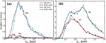
Figure 6. (a) Comparison between average numbers of S and Mo atoms sputtered from MoS2-ML under normal incidence Ne irradiation. (b) The number of sputtered S atoms under Ar and Xe ions as calculated using the SW (solid line) and REBO (dashed line) potentials.
Download figure:
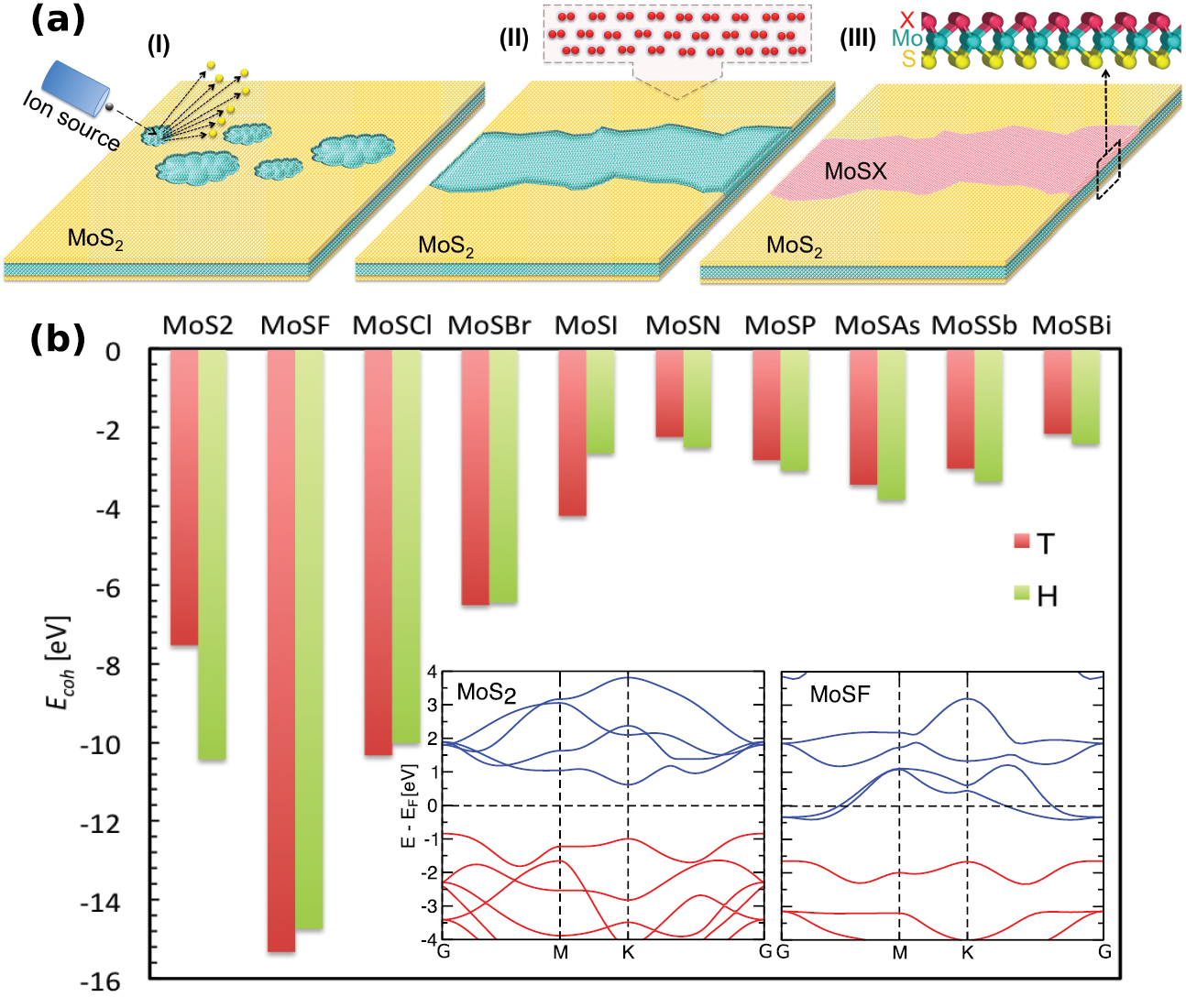
Standard image High-resolution imageDifferent numbers of S vacancies produced in the upper and bottom layers of MoS2-ML by energetic ions under specific conditions not only confirm that the preferential sputtering from one side of the MoS2 sheet can be achieved, as already experimentally demonstrated [38, 39], but also indicate that MoS2-ML can be selectively patterned with a high spatial resolution if focused ion beams can be used, e.g. in the He ion microscope [65]. If additional species are added during irradiation or after without exposing the sample to air, the missing S atoms can be substituted with other chemical elements, as schematically illustrated in figure 7(a). One can expect that in addition to S homologs Se and Te, other chemical elements can be used, and materials with different electronic properties can be manufactured.

Figure 7. (a) Schematic illustration of ion-beam mediated production of mixed MoSX material starting from MoS2-ML. The ion irradiation is used to sputter S atoms from one side of MoS2-ML, followed by an exposure to a X gas precursor. (b) Cohesive energy per primitive cell for the MoSX alloys where X stands for chemical elements from group V and VII. Inset: electronic band structures of MoS2 and MoSF alloy. The Fermi level is shifted to zero.
Download figure:
Standard image High-resolution imageTo explore this scenario, we studied energetics and electronic properties of single layers of a mixed system, when S atoms on one side of the MoS2 sheet are substituted with atoms from group V or VII. Both H and T phases were studied and the range of species is shown in figure 7. To access the stability of such compounds, we calculated cohesive energies (energy needed to dissociate the material into its individual constituent) by  , where Nx
is the number of individual constituents, Etot and Ex
are the total energy of the system and energy of its component parts, respectively. The energies proved to be negative and for several compounds comparable to that of MoS2-ML, indicating that the mixture compounds should be at least metastable, figure 7(b).
, where Nx
is the number of individual constituents, Etot and Ex
are the total energy of the system and energy of its component parts, respectively. The energies proved to be negative and for several compounds comparable to that of MoS2-ML, indicating that the mixture compounds should be at least metastable, figure 7(b).
We also calculated the energy difference between the mixed and segregated compounds, which are provided in table S4. It proved to be of the same order of magnitude (about or less than 0.1 eV per formula unit) as for the MoSSe system, that was experimentally realized, which may serve as another piece of evidence that the mixed material should be stable and will not spontaneously segregate into two compounds. Therefore, such 2D alloys can be manufactured via a post-synthesis procedure including vacancy production and atomic substitution under ion beam. Among considered compounds, MoSF was found to be energetically most favorable in accord with the recent experimental data showing the high stability of doped MoS2 samples with F-containing groups [66]. We stress that the mixed materials may be metastable with respect to dissociation into pure components, but they still could be manufactured, as ion-beam mediated engineering does not assume that the material is always in the thermodynamic equilibrium.
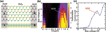
To get further insights into the electronic properties of the mixed compounds, we have analyzed the electronic structure of MoSF, presented in figures 7 and S4. Our band structure calculations showed that MoSF is a metal, see the inset in figure 7(b). Since F has an extra electron as compared to S and can be referred to as n-type dopant, the metallic behavior can be understood by a shift of the Fermi level to the conduction band. This suggests that partial substitution of S with F can be used to inject electrons into the system, and the metallic MoSF compound can serve as the electrode material attached to the semiconducting MoS2-ML. Thus the entire device can be implemented on a single sheet, avoiding the severe problems of making good electrical contacts in 2D materials. Mixed MoSCl and MoSBr compounds also proved to be metals, at least at the DFT/PBE level of theory, as shown in figure S5. To study the electronic properties of such a lateral heterostructure, we carried out electronic transport calculations through the system where the metallic MoSF compound serves as an electrode material attached to the semiconducting MoS2-ML, shown in figure 8(a). The results showed a non-linear current-voltage similar to characteristics of a resonant tunneling diode. The threshold voltage of  0.5 V reflects the energy mismatch between the Fermi level of the metallic electrodes and the lowest unoccupied levels of the channel region. In addition, the I–V plot indicates a negative differential resistance (NDR) feature at 1.37 V
  V with a peak-to-valley ratio of
  1.3 comparable to those reported for graphene-h-BN-graphene-based tunneling devices [67]. The NDR effect can be attributed to the drop in the transmission coefficient within the corresponding bias window (see figures 8(b) and (c)). This feature can be used in a number of electronic devices such as frequency multipliers and high-frequency oscillators.
Figure 8. (a) Schematic illustration of a MoSF-MoS2-MoSF based device. L and R represent semi-infinite left and right electrodes that consist of metallic MoSF-ML. The channel length of the device is 22.46  . (b) Bias-dependent transmission contour plot (c) I–V characteristics for the MoSF-MoS2-MoSF device. The arrow indicates negative differential resistance (NDR) in transmission and I-V plots.
Download figure:
Standard image High-resolution image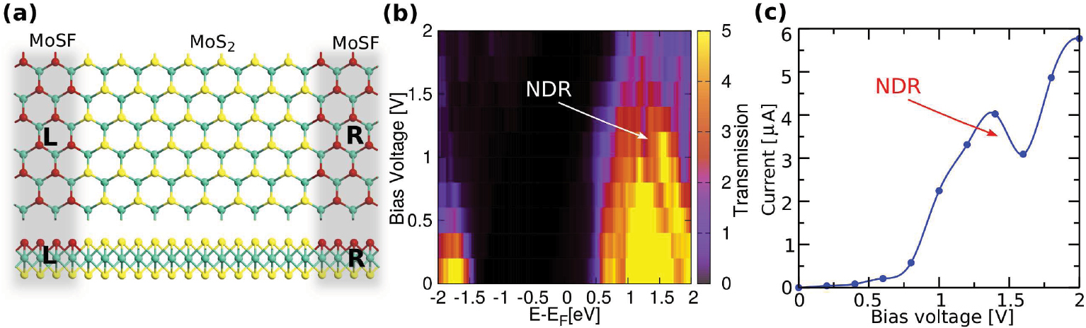
4. Conclusion
In summary, using molecular dynamics simulations, we studied the production of defects in MoS2-ML under noble gas ion irradiation. For a wide range of ion energies, in the regime where nuclear stopping dominates, and various incident angles we showed that the most prolific defects which appear under ion bombardment are S vacancies. We demonstrated that the dependence of the total number of sputtered atoms on ion energy is qualitatively the same as in other 2D materials, but it has unique features related to the tri-layer geometry of MoS2-ML and the presence of two types of atoms with drastically different masses. We anticipate similar effects to occur in ion irradiation of other layered TMDs due to analogy in the structural properties. As vacancies in TMDs have been demonstrated to be an effective tool to tailor the carrier types and optical response in these systems [68, 69], ion bombardment is the ideal tool to achieve that with high spatial resolution. We showed that depending on the angle of incidence, ion type and energy, S atoms can be sputtered away predominantly from the top or bottom layers, creating unique opportunities for engineering mixed MoSX compounds where X are chemical elements from group V or VII. Using first-principles calculations, we studied the electronic structure of such systems, and demonstrated that they can be metals. We discussed how lateral heterostructures representing metal/semiconductor/metal junctions can be designed using focused ion beams combined with the exposure of the system to a precursor gas, e.g. fluorine. We showed that MoSF-MoS2-MoSF has electronic transport properties reminiscent of those of resonant tunneling diodes, exhibiting negative differential resistance. Our results indicate that ion bombardment is a promising tool to tune stoichiometry and other properties of TMD monolayers and implement a broad range of nanoscale electronic devices via the appropriate post-growth processing of TMDs based on ion irradiation combined with the exposure of the samples to precursor gases.
Acknowledgments
We thank H-P Komsa and J Kotakoski for discussions. AVK acknowledges the Academy of Finland for the support under Project No. 286279, and the support from the US Army RDECOM via contract No. W911NF-15-1-0606. We further acknowledge the help from Dr Jin-Wu Jiang (Shanghai University) and Julian Schneider (QuantumWise) for using SW potentials of MoS2-ML. The irradiation movies are created using the Open Visualization Tool (OVITO) [70]. The computational support from the HZDR computing cluster is gratefully appreciated.