


Abstract
In this work, we exploit nanosecond laser irradiation as a compact solution for investigating the thermomechanical behavior of tungsten materials under extreme thermal loads at the laboratory scale. Heat flux factor thresholds for various thermal effects, such as melting, cracking and recrystallization, are determined under both single and multishot experiments. The use of nanosecond lasers for mimicking thermal effects induced on W by fusion-relevant thermal loads is thus validated by direct comparison of the thresholds obtained in this work and the ones reported in the literature for electron beams and millisecond laser irradiation. Numerical simulations of temperature and thermal stress performed on a 2D thermomechanical code are used to predict the heat flux factor thresholds of the different thermal effects. We also investigate the thermal effect thresholds of various nanostructured W coatings. These coatings are produced by pulsed laser deposition, mimicking W coatings in tokamaks and W redeposited layers. All the coatings show lower damage thresholds with respect to bulk W. In general, thresholds decrease as the porosity degree of the materials increases. We thus propose a model to predict these thresholds for coatings with various morphologies, simply based on their porosity degree, which can be directly estimated by measuring the variation of the coating mass density with respect to that of the bulk.
Export citation and abstract BibTeX RIS

Content from this work may be used under the terms of the Creative Commons Attribution 3.0 licence. Any further distribution of this work must maintain attribution to the author(s) and the title of the work, journal citation and DOI.
1. Introduction
Tungsten (W), thanks to its high melting point, good thermal conductivity, low sputtering yield and tritium retention, has been chosen as the reference plasma facing material (PFM) for the divertor plasma facing components (PFCs) of ITER [1]. Due to plasma–wall interactions, W PFCs can be eroded, leading to prompt W redepositing in the divertor region, or to a mixing of W with other plasma impurities and the formation of co-deposits above the first wall [2–4]. The co/re-deposited layers are usually characterized by different morphologies, structure, composition and thickness, depending on the type of first wall materials, the specific first wall position and the history of all the operating conditions [3, 5–7]. Both pristine PFMs and co/re-deposits are subjected to extreme thermal loads delivered by the edge plasma. In ITER, during transient plasma events (e.g. ELMs, VDEs and disruptions), the peak power density can reach several GW m−2 [4, 8], likely inducing catastrophic thermal effects on the plasma-surrounding materials, including recrystallization, melting, droplet ejection, surface roughening and cracking [9]. Very little is known about the behavior of co/re-deposits under these extreme thermal loads, firstly, because their composition, structural, morphological and thermomechanical properties are hard to predict, and secondly, because it is not trivial to assess the impact of these properties on behavior under high thermal loads. Co/re-deposited layers can eventually delaminate from their substrates, enter the plasma and increase dust formation, which is detrimental to both PFCs and machine operation [10, 11].
Electron beams [12–15], pulsed lasers [16–20] and plasma generators [16, 21, 22] are usually exploited at the laboratory scale as dedicated facilities for the high heat flux testing of W PFCs, both in the bulk or in the coating form, under ITER-relevant transient conditions. These techniques usually rely on the use of temporal rectangular pulsed beams with a comparable pulse duration of plasma transient events (i.e. from a few to several hundreds of microseconds), reaching similar power densities to the ones delivered by ELMs, VDEs or disruptions. Since the timescale can substantially vary between plasma transient events, a suitable parameter for comparing the various thermal effects induced by different sources is needed. From the energy balance of an irradiated surface the heat flux factor (HFF) naturally emerges [23]. This is defined as  (MJ m−2 s−0.5), or equivalently
  (MW m−2 s0.5), where Fabs is the absorbed energy fluence, Pabs is the absorbed power density and
  is the excitation pulse duration. As long as the heat transfer is governed by standard diffusion (i.e. for timescales longer than ps), the damage threshold for thermal loads can be usefully described in terms of HFF—this quantity being irrespective of the type of the heat source. Therefore, the use of HFF can also be coherently applied to nanosecond excitations. The HFF describes the maximum reachable surface temperature. For this reason, damage due to melting can be consistently assessed in terms of HFF between irradiation sources with a very different pulse duration. For a homogeneous material, free from external stresses, the thermal stress depends on the temperature gradient. For the laser irradiation of metals, in which the energy is absorbed in a very thin surface layer, the temperature profile is such that the maximum temperature gradient—so the maximum thermal stress—occurs where the temperature itself is maximum, i.e. at the surface. If the maximum stress occurring in the material overcomes some critical thresholds (e.g. the yield stress as proposed in this work), cracks can be initiated. Consequently, HFF can also be exploited to assess crack initiation thresholds. For cracking dynamics, instead, the space and time evolution of the stress, which are strictly correlated to the source pulse duration, must be taken into account. Accordingly, the HFF alone is not a sufficient comparison term for characterizing crack damage between irradiation sources with different pulse durations.
Besides being cost effective and easily accessible at the lab-scale, nanosecond lasers have already been widely adopted for fusion relevant applications, such as for laser-induced breakdown spectroscopy [24], tritium desorption of the first wall [25–27] and the laser cleaning of diagnostic mirrors [28, 29]. In addition, they have also been applied to the investigation of ablation and melting thresholds on different plasma-exposed W materials, in order to highlight the role of He bubbles on the behavior of W under extreme thermal loads [30, 31]. Recently, thermal effects induced on W by ITER-relevant thermal loads have also been mimicked by nanosecond lasers [32]. However, the experimental investigation reported in [32] was performed in the ablation regime, and it did not explicitly consider the effect of different HFFs on W, making it difficult to compare with thermal effects induced by other irradiation techniques (e.g. e-beams).
In this work, we employ nanosecond laser irradiation to study the thermal effects induced by fusion-relevant extreme thermal loads on various W materials. Irradiation is performed under the ablation regime. Since the energy associated with plasma instabilities can be delivered to the material with a time profile that can substantially differ from a rectangular distribution, interest in the constant need to test the response of materials to different thermal load conditions is continuously increasing [33]. For this purpose, we exploit a Nd:YAG laser with a Gaussian time distribution, which can mimic the nonuniform transient thermal load temporal profiles that are found in experimental fusion devices [33–35]. Bulk W samples are firstly irradiated under different laser irradiation conditions, i.e. single and multishots. The melting and recrystallization damage thresholds are assessed in terms of HFF in order to validate the use of nanosecond lasers for mimicking the thermal effects induced by fusion-relevant extreme thermal loads. Crack initiation thresholds are also proposed in terms of HFF. Damage thresholds are then investigated on the nanostructured coating proxies of different coating scenarios in tokamaks (e.g. W redeposits). The temperature and the thermal stress profiles are computed numerically by 2D thermomechanical code; this code is also adopted to predict the HFF thresholds for the various thermal effects on the different W morphologies.
2. Experimental setup
2.1. Samples
The bulk W samples are Plansee sheets 100 μm thick with a mirror-like surface finish (WML) characterized by ≈100 μm grains. The surface roughness of these samples is ≈50 nm. The samples are not chemically pre-treated before exposure. For this type of material, we consider bulk W mechanical and thermal properties (i.e.  g cm−3, E = 411 GPa,
  and
and  10−6 K−1). The surface reflectivity at
  nm is 55%. A tensile yield strength (
 ) of 1350 MPa (i.e. at room temperature) and an ultimate stress (
 ) of 1500 MPa are chosen as reference values for successive computations [33].
All the coatings are deposited by pulsed laser deposition (PLD) onto silicon (Si) wafers (1 0 0), 500 μm thick, and onto bulk W substrates, 1 mm thick. We described the sample production and characterization in previous works [37, 38]. We chose four different types of coating, namely columnar tungsten (c-W), amorphous-like tungsten (a-W), porous tungsten (p-W) and amorphous tungsten oxide (a-WO3). These coatings, due to their peculiar structure and morphology, can mimic different W coating scenarios in tokamaks [38, 39]. In particular, c-W coatings mimic the W coating on CFC tiles in machines like JET, AUG or WEST, while a-W, p-W and a-WO3 are proxies of promptly re-deposited W or co-deposited W in the presence of oxygen as gas pollution. The coating structure and morphology have been assessed by SEM (figure 1) and XRD analysis. c-W coatings are characterized by ≈16 nm crystallites, while the grains are ≈50 nm, whose orientation (i.e. (1 0 0) of α-W) is driven by the deposition process [37, 40]. All the other samples, instead, show an amorphous structure, where the crystallite size is below 2 nm [37, 40]. The coating thicknesses range from 400 nm to 2 μm.
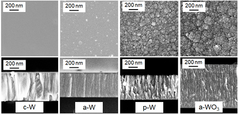
Figure 1. SEM top view and cross section images of the as-deposited W- based coatings. From the left: nanocrystalline columnar W (c-W), amorphous-like W (a-W), porous W (p-W) and amorphous-like WO3 (a-WO3).
Download figure:
Standard image High-resolution image2.2. Sample pre- and post-irradiation characterization
The total optical reflectance R of the as-deposited samples, needed for the computation of Fabs (i.e.  ), therefore for the determination of HFF, is evaluated by a UV–vis–NIR PerkinElmer Lambda 1050 spectrophotometer with a 150 mm diameter integrating sphere. The morphology evolution after irradiation is investigated by a Zeiss Supra 40 field emission scanning electron microscope (SEM) with an accelerating voltage of 3–7 kV, and by optical microscopy. Energy dispersive x-ray spectroscopy analysis is performed to obtain information about the elemental composition of the samples. A thermoscope atomic force microscope (AFM), operating in non-contact mode, is exploited to assess surface roughness before and after irradiation. W oxidation is monitored by Raman analysis. Raman spectra are collected at room temperature by a Renishaw inVia microRaman spectrometer with a 514.5 nm laser wavelength and approximately 1 mW of laser power on the sample. The spectra resolution is about 3 cm−1.
The retained oxygen concentration in the metallic W coatings is determined by EDS analysis, resulting in <10% for c-W and ≈25% for a-W, while it is ≈55% for p-W. The elastic properties (i.e. Young's modulus E, Poisson's ratio ν and shear modulus G) and the coefficient of thermal expansion α of the coatings were determined by the combined use of Brillouin spectroscopy and the substrate curvature method in previous works [40, 41]. They are summarized in table 1. No information about the elastic properties of the a-WO3 sample is available yet. The mass density (ρ) of the coatings, reported in table 1, was determined by the combined use of crystal quartz microbalance measurements during deposition and by EDS analysis [37, 42]. All these properties are taken as input parameters for the numerical model.
Table 1. Main thermophysical properties of the various samples analyzed in this work.
| Sample | E (GPa) [40] | ν [40] | G (GPa) [40] | α (10−6 K−1) [41] | ρ (g cm−3) [37] |  (MPa) (MPa) |
 (MPa) (MPa) |
Dk (cm2 s−1) |
|---|---|---|---|---|---|---|---|---|
| bulk-W | 411 | 0.28 | 160 | 4.2 | 19.25 | 1350 [33] | 1500 | 0.696 |
| c-W | 360 | 0.285 | 130 | 5.1 | 18 | 1260 | — | 0.642 |
| a-W | 150 | 0.34 | 50 | 7.8 | 11 | 770 | — | 0.397 |
| p-W | 110 | 0.42 | 40 | 8.9 | 9 | 630 | — | 0.325 |
| a-WO3 | — | — | — | — | 5 | 350 | — | 4.9 10−3 |
The surface roughness of the samples deposited on both the flat Si and bulk W substrates well replicate the substrates, measuring about 0.7 nm for the compact coatings (i.e. c-W and a-W), while it is ≈1.2 nm for the porous morphologies (i.e. p-W and a-WO3) on Si, and around 20–40 nm for the coatings on the bulk W substrates. Finally, the total surface reflectance R at  nm is 58% for the c-W coatings, 55% for a-W and 22% for p-W. At
  nm the total reflectance of the a-WO3 coatings is ≈18%.
2.3. Laser irradiation
Laser irradiation of the bulk W and metallic W coatings is performed by exploiting the fundamental harmonic ( nm) of a Q-switched Nd:YAG laser. In the case of a-WO3 coatings, instead, due to their optical transparency in the IR region, the samples are irradiated by the second harmonic (
 nm) of the same laser system. The temporal Gaussian profile of the laser is characterized by a
  of 7 ns. The laser beam enters a vacuum chamber and strikes the sample surface with an angle of incidence of 45° (see figure 2). The beam spot has an elliptical shape with a total area of 0.81 cm2. The laser intensity profile is a top-hat (see figure 3(a)), with evident inhomogeneities localized at the boundary of the spot. For this reason, all the analyses are taken in the spot center, where the intensity profile is almost homogeneous, in order to avoid any instrumental influence on the thermomechanical behavior induced by intensity nonuniformity. The total beam transmittance along the optical path is
  80%. The samples are irradiated with different laser energy fluences, which vary between 50 mJ cm−2 and 3.5 J cm−2. In this way, a broad range of HFFs is spanned. The irradiation is performed at room temperature and under vacuum conditions (i.e. 1 Pa base pressure). The sample surface temperature during nanosecond pulses cannot be measured by our experimental system. For this purpose, numerical simulations (see below) are performed.

Figure 2. Experimental setup for laser irradiation.
Download figure:
Standard image High-resolution image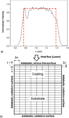
Figure 3. (a) The laser intensity spatial profile (black line) and simulated spatial intensity profile (dotted red line). All the analysis proposed in this work is considered in the spot center, where the intensity profile is almost homogenous. (b) The numerical domain for the thermomechanical problem. The boundary problem is highlighted. Adiabatic boundaries for the heat equation are considered. For the mechanical problem, instead, a stress-free surface and radiative boundaries are taken into account.
Download figure:
Standard image High-resolution image3. Laser-induced thermal effect modeling
Numerical thermal effect thresholds for melting, recrystallization and cracking following nanosecond pulse excitation can be obtained by solving the coupled heat and dynamic displacement equations. In our model, we neglect the thermoelastic effect, so that the heat equation can be solved first, and then from the computed temperature field, the thermal stresses can be obtained. We do not consider any surface or material modifications after irradiation. The main governing equations, for a 2D Cartesian isotropic model, can be written as:
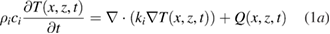
where the x-axis and the z-axis are taken along the surface and the thickness respectively, T is the temperature, k is the thermal conductivity, c is the specific heat, Q is the laser power density,  is the total displacement field and σ is the stress tensor. The subindex i refers to the i-layer for which the two equations are solved (i.e. coating and substrate). Inside the i layer, the thermal diffusivity Dk is defined as
  . In accordance with our experimental setup, we consider a Gaussian laser with a rectangular spatial distribution exponentially damped along the z direction [43, 44] (see figure 3(a)):
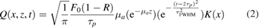
where F0 is the incident laser fluence (J cm−2) and  (cm−1) is the absorption coefficient. The extinction length (lp) scales as 1/
 , and in the case of metals it is typically of a few tens of nm. The rectangular spatial distribution
  has a characteristic dimension of D = 0.9 cm, which is the elliptic beam spot major axis. The laser strikes at z = 0 on the sample surface (see figure 3), and its energy is then converted into heat, which propagates along the x and z directions following equation (1a). Within the pulse duration
  , the heat diffuses till a depth of the order of
  . At the end of the pulse, the energy fluence Fabs will have heated a layer with a depth of lth, inducing in that layer an average temperature increase which scales as the
  . For a rectangular temporal profile the fluence is simply given by
  , such that
  . For temporal profiles that are different from the rectangular one, the choice of
  for the computation of HFF is, to some degree, arbitrary. In this work we choose
  in order to have the same maximum surface temperature rise (
 ) for a fixed fluence F0, i.e. the temperature of the hot-spot, as the one obtained by a rectangular profile.
  can be easily calculated from analytical solutions of the 1D heat equation. In the case of a Gaussian profile it can be expressed as [45]:
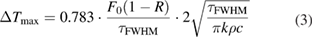
where the factor 0.783 is obtained by integrating the Gaussian excitation over time. By comparing this relation with that of the proper rectangular profiles (i.e.  [45]), it is clear that in order to have the same
  ,
,  . Thanks to this choice, the Gaussian and rectangular pulses with the same HFF result in the same temperature rise, irrespective of the pulse duration.
In contrast, the resulting temperature gradient depends on the pulse duration. The temperature gradient induces a dynamic stress field, described by equation (1b), which can be significantly different between the ms and ns laser pulses. By considering an isotropic, linear elastic material, only three components of the stress tensor σ have to be considered, namely the two normal stress components ( and
and  ) and the shear stress
  . By taking into account the stress-displacement relationships and the force equilibrium conditions, these stress components can be written in terms of the displacement field as [46]:
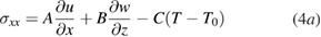
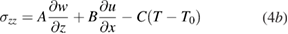
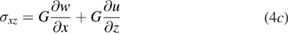
where  ,
,  and
and  are material constants and T0 is the baseline temperature; u and w stand for the displacement along the x and z directions respectively. In this model we do not consider any temperature dependence of the elastic properties. For our computations we only consider the room temperature values summarized in table 1.
Equations (1) and (4) are finally solved together with the suitable boundary conditions. In particular, for the heat problem, all the boundaries are treated as adiabatic surfaces (i.e. no heat radiation out of the domain). For the mechanical problem, instead, a stress-free surface condition is applied at z = 0, while the remaining boundaries are considered as fictitious numerical boundaries, to which classic Sommerfeld radiation conditions are applied (i.e. one-way wave equations). For both the thermal and the mechanical equations, we assume a perfect matching condition (i.e. no contact resistance) between the two following layers. This, in turn, results in the continuity of both the heat flux and the displacement field at the layer interface.
The thermomechanical problem is thus solved numerically by a classic Eulerian explicit finite difference method for a fixed mesh of equally spaced Δx and Δz nodes (see figure 3). The node spacing Δz is fixed at 3 nm, such that a suitably large number of nodes can be exploited to describe the penetration depth of the source along the z-direction, while  is about 0.1 mm. Each time step corresponds to a
  of ≈1 ps.
Taking into account the temperature dependance of k and c as the one reported in [47], and an absorption coefficient of 1.46 106 cm−1 at  nm [48], the numerical HFF thresholds for bulk W melting and recrystallization are obtained, from equation (1a), if the maximum temperature reaches 3690 K (i.e. a melting temperature of W) and 1400 K (i.e. the recrystallization temperature of W) respectively. Over the melting temperature, a constant thermal conductivity of 0.7 W cm−1 K−1 and a constant specific heat of 0.23 J g−1 K−1 are considered for liquid W [49]. The absorption coefficient can then be drastically affected by many factors, such as the porosity degree and surface oxidation, which, altering electron conductivity, can lead to higher laser extinction lengths [31]. This increase can be roughly estimated as a function of the mass density, being the extinction length
  , where
  is the plasma frequency. This means that for porous coatings, for which the highest decrease of ρ is measured, lp increases by about 60% with respect to that of bulk W. However, even in the worst case, lp remains significantly lower than the heat penetration length. All possible skin effects can thus be disregarded, and for simplicity, the bulk W absorption coefficient is considered for all simulations, including the case of nanostructured coatings. As shown in figure 4, the melting threshold obtained for bulk W by our numerical simulations is ≈58.7 MW m−2 s0.5. Recrystallization, instead, is achieved at HFF = 18.8 MW m−2 s0.5.
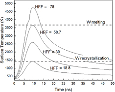
Figure 4. Temperature profiles computed for bulk W with different HFFs. The numerical thresholds for recrystallization and melting are highlighted.
Download figure:
Standard image High-resolution imageFrom the mechanical problem (equation (1b)), the cracking threshold can be estimated. For this purpose, we rely on the theoretical model developed by Arakcheev et al in [50] for the cracking threshold determination under the plane stress approximation for an ideal elasto-plastic material (i.e. no hardening). This approximation fits our case well, since the thickness of the irradiated sample is much smaller than its lateral dimension and the laser spot size. Following the model, at least three conditions for crack formation can be identified, namely: (i) if the temperature exceeds the ductile-to-brittle transition temperature (DBTT), (ii) if, when  , the maximum thermal stress exceeds the ultimate stress of the material and (iii) if, when cooling down at
  , the maximum thermal stress is higher than the yield strength. In our simulations, both the yield and the ultimate stress are considered temperature-independent. For the bulk W properties reported in table 1 and considering a DBTT of 673 K, we find a cracking threshold of ≈12.9 MW m−2 s0.5, which corresponds to a critical temperature value of ≈1073 K. This value fits well both the experimental and numerical data that can be found in the literature [51].
In the case of coatings, no experimental information about the thermal diffusivity (Dk) is available. It is not reasonable to take the same Dk as bulk W, since the high void fraction (and hence the lower density) of the coatings can imply in some way a variation of Dk. In particular, the higher the porosity degree (DP), the lower the Dk [52, 53]. Here, we propose an estimate of DP starting from the mass density variations, as:
so that a simple approximation of the reduced thermal diffusivity of the coatings can be determined as:

From equation (6), the various Dk values of the coatings reported in table 1 are calculated. In the case of a-WO3, the reference bulk values are chosen according to [54] (i.e.  g cm−3, Dk = 7.4 10−3 cm2 s−1). In the case of coatings, Dk is considered temperature-independent. This approximation of Dk is valid as far as the chemical nature of the sample remains the same. This means that it cannot be applied, for example, to WO3 coatings starting from the diffusivity of bulk W. Moreover, the physical meaning of this parameter considers the medium as composed of bulk parts and voids, such that thermal diffusivity is evaluated as an average equivalent property. When the morphology becomes really open and strongly oriented features (e.g. cauliflower morphologies) or hierarchical structures appear, the single features can have completely different properties, such that the concept of an equivalent homogeneous medium can lose its validity.
The same approximation exploited for Dk is also adopted for the derivation of reduced ultimate and yield stresses of the coatings, which are strictly related to the porosity degree of the material (i.e. they decrease and DP increases) [55], so that  and
and  . The calculated values are reported in table 1. The DBTT, instead, is kept fixed to the bulk W value.
4. Experimental results and discussion
4.1. Bulk W irradiation
We first investigate the thermal effects induced by nanosecond laser irradiation on bulk W samples. The surface of unirradiated WML is shown in figure 5(a). WML is irradiated with absorbed HFFs ranging from 3 MW m−2 s0.5 to 78 MW m−2 s0.5. Surface cracking is observed between 14 and 18 MW m−2 s0.5 (figure 5(b)). Below this cracking threshold, no surface modification is detected. Even if localized surface melting evidence is found at 36 MW m−2 s0.5 at the edges of surface imperfections and cracks (figure 5(c)), the HFF melting threshold is considered at 55.5 MW m−2 s0.5, where the W surface is more widely melted (figure 5(d)). The spot area is completely melted above 62 MW m−2 s0.5, where droplet formation also occurs (figure 5(e)). At 78 MW m−2 s0.5, surface nanostructuring is found inside the melted regions (figure 5(f)). Probably due to the pristine large grains (i.e. micrometric grains) of W, no recrystallization is found.
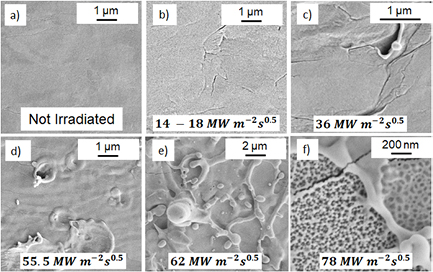
Figure 5. SEM images of bulk WML before and after nanosecond one-shot laser exposure at different HFFs. (a) Unirradiated surface, (b) cracking threshold, (c) localized melting, (d) melting threshold, (e) droplet formation and (f) surface nanostructuring. All the images are taken in the center of the laser spot.
Download figure:
Standard image High-resolution imageBulk W behavior under a high number of thermal cycles is investigated. Irradiation is performed with the laser always striking in the same sample position with a repetition rate of 10 Hz. If irradiation is performed at 10 MW m−2 s0.5, which is well below the single shot cracking threshold (i.e. 14 MW m−2 s0.5), no surface damage is observed, even after 18 000 pulses (figure 6(a)). In these irradiation conditions, indeed, the maximum numerically estimated temperature is ≈650–700 K, which is very close to the DBTT value of W. Therefore, only elastic deformation takes place, such that the total stress cannot exceed the yield stress, and cracks cannot initiate or propagate. Cracking is firstly found starting from 11.5 MW m−2 s0.5 after 100 shots (figure 6(b)). After 100 pulses at 21 MW m−2 s0.5, clear recrystallization occurs (figure 6(c)). Surface melting, instead, is observed after 100 cycles between 31.4 and 36 MW m−2 s0.5 (figure 6(d)). In general, as HFF increases, fewer pulses are needed to induce cracking, recrystallization or melting. The observed surface damage as a function of the number of shots and the HFF is shown schematically in figure 7. As can be seen, melting occurs at a very low HFF with respect to single shot irradiation. It is well known that the threshold damage for laser irradiation is drastically lowered by an increasing number of performed shots. This is mostly due to the laser-driven material surface modification after each shot, which, by altering the morphology (e.g. surface roughness), induces local centers of absorption that significantly increase the local absorbed laser energy.
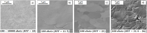
Figure 6. SEM images of bulk WML after multishot nanosecond laser irradiation. The various HFF thresholds after 100 shots are highlighted. All the images are taken in the center of the laser spot.
Download figure:
Standard image High-resolution image
Figure 7. Thermal effects observed after a different number of laser shots and a different HFF. The green line shows the limits of the damage threshold area, while the black line shows the limits of sub-melting damage.
Download figure:
Standard image High-resolution imageIn table 2, the HFF thresholds reported in the literature for various bulk W materials, under both single and multishot irradiation by millisecond laser and electron beams, are reported. These thresholds are compared to the ones obtained in this work by nanosecond laser irradiation and by our numerical model. As can be seen, the results are in good agreement, confirming the effectiveness of the HFF parameter in determining the material behavior under thermal loads, regardless of the type of source exploited. The specific microstructure of W and its composition, as well as the environmental conditions, can deeply affect the thermomechanical response of the material. For this reason, unique threshold values for the different thermal effects cannot be found. Moreover, the experimental values found in this work for the single shot irradiation well fit the numerical ones. This confirms the validity of the simplified hypothesis, which is taken into account in the model. The little discrepancy can be attributed to surface imperfections or intensity spikes in the laser profile, as well as to other environmental factors (e.g. radiative thermal losses from the heated surface), which are not taken into account in the simulations.
Table 2. Experimental HFF (MW m−2 s0.5) thresholds reported for different bulk W samples under single shot and multishot irradiation by electron beams and millisecond lasers at room temperature. The various HFF thresholds are compared with the ones obtained in this work by nanosecond laser irradiation for both single and multishot conditions and by numerical simulations.
| Number of shots | Melting | Recrystallization | Cracking |
|---|---|---|---|
| Single-shot | >50 ([36], e-beam) | 23–39 ([36], e-beam) | 18 ([51], e-beam) |
| Single-shot (This work) | 55.5 | — | 14–18 |
| Single-shot (This work, model) | 58.7 | 18.8 | 12.9 |
| Multi-shots | 30 ([57], e-beam, 100) | 15–24 ([17], ms laser, 500) | 12 ([57], e-beam, 100) |
| Multi-shots (This work) | 31.4–36 (100) | 15 (500) | 11.5 (100) |
4.2. W-based coating irradiation
Thanks to their highly localized energy absorption around the surface (i.e. the laser extinction length for metals ≈20 nm), lasers can be consistently exploited for the irradiation of coatings, without promoting, as it happens in the case of electron beams, bulk heating effects that directly involve the heating of substrate materials. Here we focus on the various thermal effects induced by laser irradiation on different nanostructured W coatings. Being representative of W coatings and co/re-deposited layers in tokamaks, their investigation under high thermal loads is crucial to the assessment of their thermomechanical response to critical transient heat loads, which is not completely understood, and which can be found in fusion reactors.
Microscopy images of unirradiated c-W, a-W, p-W and a-WO3 coatings are shown in figures 8(a)–(d). After single shot irradiation, cracking occurs at very different HFF thresholds (figures 8(e)–(h)). In particular, between 16 and 20 MW m−2 s0.5 for columnar coatings, between ≈3.3 MW m−2 s0.5 and 5.6 MW m−2 s0.5 for amorphous-like coatings and below 2.7 MW m−2 s0.5 for a-WO3 coatings. Due to their high surface roughness, it is not easy to detect surface cracking in the case of porous W coatings. In this case delamination is usually observed starting from ≈3.6 MW m−2 s0.5. Rescaling the HFF thresholds obtained for a-W, p-W and a-WO3 to power densities related to a 0.1 ms transient plasma event, we ascertain that coating proxies of co-redeposits can be damaged at 0.27–0.36 GW m−2. These power densities are below those estimated for ELMy H-mode during the non-nuclear phase of ITER (i.e. above 0.45 GW m−2) [4]. In contrast, c-W better behaves under these thermal load conditions, showing a cracking threshold that is slightly higher than the one of bulk W. The threshold we obtain is very close to those reported for different W coatings under high heat flux tests at room temperature (i.e. above 20 MW m−2 s0.5) [14, 51, 58]. The higher cracking threshold with respect to bulk W samples can be attributed to the columnar grains and their preferential orientation, which help mitigate cracking, improving the thermomechanical resistance of the material [14, 51, 58].
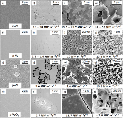
Figure 8. Single shot SEM images of irradiated nanostructured W-based coating. Metallic W coatings (i.e. c-W, a-W and p-W) are irradiated at  nm, while a-WO3 at
  nm. All the images are taken in the center of the laser spot.
Download figure:
Standard image High-resolution imageEven if local recrystallization for c-W begins at around 19.5 MW m−2 s0.5, at 29.7 MW m−2 s0.5 micrometric grains are uniformly found inside the irradiation area (see figure 8(i)). In these irradiation conditions, the temperature of the silicon substrate exceeds its melting temperature (i.e. 1600 K), and wide cracks full of melted substrate material appear on the surface. In the case of bulk W substrates, this clearly does not happen. For a-W and p-W, instead, no evidence of recrystallization can be observed by microscopy analysis. In contrast, at 10 MW m−2 s0.5 and 5.4 MW m−2 s0.5, respectively, even if the numerically estimated temperature is around the recrystallization temperature of W (i.e. ≈1350 K), sub-micrometric bubbles, around 80–100 nm in size, appear on the surface (figures 8(l)–(m)). Since bubbles are not observed in the case of c-W, which is the most compact morphology and with the lowest O2 content, their formation is thus clearly enhanced by the oxygen content retained in the material. As expected, nanobubbles are also found in the a-WO3 coatings, starting from HFF = 11.7 MW m−2 s0.5 (figure 8(n)). Thanks to Raman analysis, recrystallization of a-WO3 can be assessed. In figure 9(a), the Raman spectra recorded for the as-deposited a-WO3 coating after single shot irradiation at 5.4 MW m−2 s0.5 are shown. As can be seen, the two broad bands that characterize the WO3 amorphous phase start evolving under recrystallization in more defined peaks, which in this case, is associated with the monoclinic phase of WO3 [59, 60]. Since a-WO3 is optically transparent, the main peak of the Si substrate at 521 nm can also be detected.

Figure 9. (a) Raman spectra acquired for as-deposited a-WO3 (black line) and after single shot irradiation at 5.4 MW m−2 s0.5 (blue line). The high intensity peak at 521 nm is the main peak of the Si substrate. (b) The Raman spectra acquired for metallic c-W, a-W and p-W coatings after single shot irradiation above the melting threshold.
Download figure:
Standard image High-resolution imageSurface melting of c-W occurs at 47–54 MW m−2 s0.5 (figure 8(o)). This value is really close to the melting threshold of bulk W (i.e. 55.5 MW m−2 s0.5). In contrast, melting starts at much lower HFFs for the other coatings, namely ≈23.4 MW m−2 s0.5 for a-W, above 19 MW m−2 s0.5 for p-W and above 7.8 MW m−2 s0.5 for a-WO3 (figures 8(p)–(r)). This consistent melting threshold drop is evidently mainly attributed to the drop in thermal diffusivity. In the case of p-W, over the melting threshold peculiar nanostructures, with a shape resembling a fuzzy-like W, form on the surface (see figure 8(q)). In particular, at 19.2 MW m−2 s0.5 these nanostructures extend to a thickness of ≈20 nm (see figure 10). Their formation is strictly related to the native surface roughness of p-W coatings, which is enhanced by the explosion of nanobubbles above a certain temperature. It has to be remembered that coatings with very different thicknesses have been irradiated. No substantial differences in the damage thresholds are observed for thicknesses down to 500 nm, where the influence of the substrate material, in particular in the case of Si, clearly affects the coating damage.
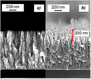
Figure 10. SEM cross section images of p-W coating before (a) and (b) and after (c) and (d) irradiation. The fuzzy-like nanostructure formation is highlighted.
Download figure:
Standard image High-resolution imageSurface roughening is assessed by AFM analysis. A remarkable roughness increase for c-W is observed at HFFs close to the melting threshold, where the Rq goes from 0.7 nm to 1.1 nm for the Si substrate, and from 40 nm to ≈70–90 nm for bulk W substrates. At the melting threshold, for the other coatings it increases by up to six times the initial Rq values. Generally, below melting, surface roughening is negligible.
Since a high trapped oxygen content is found for the different nanostructured metallic W coatings, Raman analysis is also performed after irradiation above the melting thresholds on all the metallic samples, in order to detect possible laser-induced oxidation of the material. The spectra are summarized in figure 9(b). All the as-deposited metallic W coatings show a flat spectrum. For c-W, this spectrum remains unchanged after irradiation at any HFF. This is not the case for a-W and p-W coatings. As can be seen, for a-W and p-W, two shallow broad bands become visible over the corresponding melting thresholds (i.e. 23.4 and 19.2 MW m−2 s0.5 (red and blue spectra)). These two broad bands can be attributed to the formation—even in a small quantity—of an amorphous sub-stoichiometric W-oxide layer on the surface of the sample. The different stoichiometric ratio, with respect to a-WO3, is highlighted by the different spectra shapes observed for a-WO3, p-W and a-W coatings. The absence of the Si peak, instead, confirms the surface nature of the oxide layer, since the probing laser can pass through the transparent oxide coating, while it is completely absorbed in the first few nanometers of the underlying metallic material. Since irradiation is always performed in vacuum conditions, it is the high oxygen content initially present in the coating that can lead to the formation of W-O bonds when the temperature of the material is sufficiently high to trigger diffusion processes and recombination within the melted layer.
The melting and the cracking thresholds obtained for the various nanostructured W coatings are summarized and compared with the ones derived by our numerical model in table 3. All the experimental melting thresholds are in quite good agreement with the numerical predictions. This highlights the fact that, by simply considering the effect of the porosity degree of the coatings on their thermal diffusivity, realistic predictions of the melting of various nanostructures can be obtained. The porosity degree also allows an estimation of the ultimate and the tensile stresses of the coatings, which are required to obtain the cracking thresholds. As can be seen, for a-W, the experimental and numerical values are in good agreement. In this case, since the material is mechanically isotropic, the approximations made for  and
and  , together with the hypothesis made in the model, well represent the real mechanical behavior of the material. In the case of c-W, instead, a higher discrepancy between the two thresholds is observed. This is basically related to the mechanical anisotropy of the c-W coatings, which is observed along the growth direction (i.e. along the columns), and which is not taken into account in the model.
Table 3. A comparison between the experimental and numerical HHF thresholds for melting and cracking for the single shot irradiation of nanostructured W coatings.
| Melting (MW m−2 s0.5) | Recrystallization (MW m−2 s0.5) | Cracking (MW m−2 s0.5) | |
|---|---|---|---|
| Sample | Exper.—Num. | Exper.—Num | Exper.—Num |
| c-W | 47–55 / 54.8 | 19.5–29.7 / 18 | 16–20 / 11 |
| a-W | 23.4 / 27.4 | — / 9.4 | 3.3–5.6 / 3.5 |
| p-W | 19.2 / 20 | — / 6.6 | — / 1.7 |
| a-WO3 | >7.8 / 7.8 | 5.4 / 3.3 | 2.7 / — |
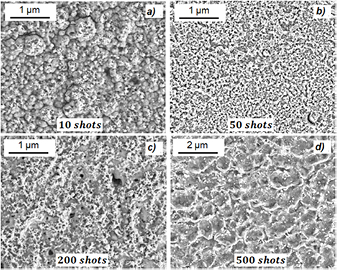
The coatings are finally tested up to 500 shots (f = 10 Hz) with HFFs ranging from 1 to 12 MW m−2 s0.5. Even in this case we observe a drop in the different damage thresholds as the number of pulses increases. In the case of c-W coatings, the damage threshold after 500 shots is 6.2 MW m−2 s0.5. Increasing the HFF to 7.8 MW m−2 s0.5, c-W starts cracking after 200 pulses. Melting and delamination occur at 12 MW m−2 s0.5 starting from 100 pulses. After 500 pulses in these irradiation conditions, a major fraction of the coating is delaminated. In the case of a-W, p-W and a-WO3 coatings, surface damage is always found after 500 shots at any HFF value between 1 and 12 MW m−2 s0.5. In general, a consistent fraction of the coatings delaminates after 100 pulses between 2 and 3.1 MW m−2 s0.5. This could be a crucial aspect in the tokamak environment, since all the delaminated layers can enter the plasma, migrate and add to the dust inventory, which is a critical issue for both machine and PFC operations. Particularly interesting is the evolution of the fuzzy-like nanostructures formed on p-W under multishot irradiation (figure 11). Their formation, in contrast to the single shot threshold of ≈19 MW m−2 s0.5, occurs in localized areas after only 10 shots at 3.1 MW m−2 s0.5 (see figure 11(a)). Increasing the shot number to 50, results in the complete melting of the surface, and fuzzy-like nanostructures are uniformly found above all the surfaces (figure 11(b)). After 200 shots, they start to evaporate, such that after 500 pulses, a compact melted W layer is obtained (figures 11(c)–(d)).
Figure 11. SEM images of multishot irradiated p-W at 3.1 MW m−2 s0.5 after (a) 10, (b) 50, (c) 200 and (d) 500 shots.
Download figure:
Standard image High-resolution image
5. Conclusions
In this work we investigate the thermomechanical response of bulk W and W-based coatings to high heat fluxes induced by nanosecond laser irradiation. We validate that compact, cost-effective nanosecond lasers, which are easily accessible at the lab-scale, can be exploited to test the thermomechanical behavior of materials, in both the bulk and the coating form, under fusion-relevant extreme thermal loads. Here, we exploit a laser with a Gaussian time profile, which can mimic the nonconstant time distribution of the energy delivered by plasma transient events that are found in many experimental fusion devices. Consequently, we extend the concept of the heat flux factor to Gaussian excitations by choosing a suitable pulse duration that allows easy comparison with rectangular time profiles. Thanks to this definition, we demonstrate that similar experimental thresholds for various thermal effects are found for rectangular millisecond sources and Gaussian nanosecond lasers. The experimental results are also in accordance with the numerical ones obtained by our 2D thermomechanical code.
We thus determine the thresholds for the different thermal effects of nanostructured W coatings, which can mimic various coating scenarios in tokamaks. In particular, we find from the experiments that all the coatings show lower damage thresholds with respect to bulk W. We thus implement a simple method in our numerical model to predict the thermomechanical response of nanostructured coatings to fusion-relevant thermal loads, by considering the effect of the porosity degree on the various material properties (i.e. thermal diffusivity, ultimate and yield stresses). The obtained numerical thresholds for melting and cracking are found to be in good agreement with the experimental ones.
Finally, we find that amorphous, porous and W-oxide coatings, which are proxies of co-redeposits in tokamaks, can easily crack and delaminate from their substrates even at HFF = 3.1 MW m−2 s0.5. This value, if rescaled to a 0.1 ms plasma transient event, corresponds to a power density of ≈0.3 GW m−2, which is lower than the expected power density of ELMs, VDEs and disruption in the ELMy-H mode of ITER. Since all the delaminated coatings can enter the plasma, migrate and add to the dust formation inventory, with consequently dramatic effects on ITER operation, we will further investigate the behavior of W coatings under different thermal loads conditions, possibly also in combination with linear plasma exposure.
Acknowledgments
This work has been carried out within the framework of the EUROfusion Consortium and has received funding from the Euratom research and training programme 2014–2018 under grant agreement no. 633053. The views and opinions expressed herein do not necessarily reflect those of the European Commission. The research leading to these results has also received funding from the European Research Council Consolidator Grant ENSURE (ERC-2014-CoG no. 647554).