


Abstract
We study spatially trapped ensembles of dipolar excitons in coupled quantum wells by means of photoluminescence and photocurrent spectroscopy. The photogenerated excitons are confined in very clean GaAs double quantum well structures and electrostatically trapped by local gate electrodes. We find that the common approach of electrostatic trap geometries can give rise to an in-plane imbalance of charge carriers especially when an over-barrier excitation is utilized. The excess charge carriers can give rise to an effective parabolic confinement potential for the excitons. In photoluminescence spectra, we identify the emission of both neutral indirect excitons and states influenced by the excess charge carrier density. We find that the charge imbalance in the excitonic ensemble strongly influences the radiative lifetimes of both. Our findings shine a new light on the properties of trapped dipolar exciton ensembles. This is of significant relevance to common interpretations of experimental results in terms of signatures for the formation of 'dark' and 'gray' excitonic condensates.
Export citation and abstract BibTeX RIS
1. Introduction
The research on fundamental many-body interactions and correlations in cold bosonic ensembles is an ongoing and very active field with stimulating experiments on ultra-cold atom gases [1–5] as well as on solid state exciton [6–10] and exciton-polariton ensembles [11, 12]. In particular, excitons and exciton-polaritons hosted in semiconductor heterostructures exhibit a rich variety of different many-body correlations and phases [13–15]. Hereby, indirect excitons (IXs) in coupled quantum wells (CQWs), also referred to as dipolar excitons, represent a model system with widely tunable properties to study interaction-driven phenomena such as a phase transition to a Bose–Einstein condensate (BEC) at low temperatures [16]. The critical transition temperature for a BEC is predicted to be in the order of 1 K [17], which is several orders of magnitude higher than for a BEC of atomic gases [2]. Even though promising experimental results are reported [18–20], an unambiguous proof for an excitonic BEC is still missing and motivates detailed experimental investigation of parameters influencing the interactions in exciton ensembles [21, 22].
The creation of dense exciton ensembles is a key challenge towards the experimental realization of an excitonic BEC. A promising way to realize dense IX ensembles is their spatial confinement by controlling the lateral potential landscape of the IXs. Most experimental approaches rely on field-effect devices with laterally structured electrodes on the top surface of a GaAs-based CQWs heterostructure [23–29]. The local top electrodes exploit the quantum confined Stark effect (QCSE) to trap the excitons, because the dipolar excitons are electrostatic high-field seekers [30, 31]. For very small trap electrodes and very low excitation powers, the confinement of few excitons down to trapping of a single IX has been demonstrated [23]. For such small traps, the interplay between the exciton binding energy and the dielectric screening properties of the semiconductor heterostructures gives rise to an effective parabolic potential [23]. Intriguingly, also for larger traps with a lateral extension of several micrometers and thousands of IXs, a parabolic confinement has been reported [19]. This observation is surprising since the electrostatic depletion length in the utilized semiconductor heterostructures is only on the order of hundred nanometers. In turn, a box-shape potential is expected for large exciton traps. Moreover, electrostatic traps are prone to potential fluctuations that can limit their functionality [28]. In particular, a lateral inhomogeneity of the electric field can induce the dissociation of the dipolar excitons [28, 32]. For this reason, in-plane and out-of-plane flow of excess charge carriers is possible in such electrostatic trap geometries. As a direct consequence, the introduced decoherence [33] and the loss of exciton oscillator strength [34] makes it experimentally challenging, but not impossible to detect the phase-coherent properties of such charged IX ensembles [35]. As soon as excess charge carriers are coexistent to the excitons, a second emission line emerges. The corresponding exciton complexes have been attributed to so-called trion states with a neutral exciton being bound to a free charge carrier [24, 35–49], albeit recent theory and experiments point out an alternative explanation in terms of attractive and repulsive exciton-polaron branches of excitons being dressed with the interaction with excess charge carriers [50, 51]. Generally, it is unclear whether such exciton complexes impairs the formation of a BEC of trapped composite boson ensembles.
Here, we explore the microscopic origin resulting in effective parabolic potential landscapes of exciton traps. We find evidence that the parabolicity is linked to the presence of excess charge carriers. In photoluminescence spectra, we detect two distinct emission peaks. The first emission peak (FEP), which is typically referred to as the neutral IX, and a second emission peak (SEP) several meV below the FEP. In the trion-picture, this SEP is consistent with positively charged trions, and a finite photocurrent indicates a macroscopic charge imbalance within the traps. Especially in the limit of very low excitation power, the SEP and the photocurrent depend on the specific laser spot position on the traps with distinct differences between the trap-center and trap-edge. The necessary excess charge carriers seem to stem from an IX dissociation at the trap-edges. Control experiments demonstrate that the photocurrent originates from the in-plane propagation of the excess charge carriers, which is consistent with the fact that the high-quality heterostructures are designed to omit vertical leakage currents. Moreover, the SEP is much more pronounced, when the exciton ensembles are co-illuminated with a non-resonant laser at a high excess energy. Such a high energy illumination scheme has been used in several experiments before to generate excess charge carriers [52]. Intriguingly, we find that the occurrence of the SEP has a non-trivial influence on the FEP lifetime, which cannot be described by a simple single-particle model. In this respect, our results are of great relevance for the interpretation of recent experiments on exciton ensembles, where the change of lifetime and population dynamics of IXs are interpreted in terms of a transition to dark and gray condensates at low temperatures [18, 19].
2. Experiment
The CQW sample consists of a pair of 7 nm wide GaAs QWs separated by 6 nm of Al0.33Ga0.67As and encapsulated between two 10 nm thick Al0.33Ga0.67As barriers. This unit is surrounded between two GaAs/AlAs superlattices (SLs) with the purpose to suppress vertical tunneling processes. All over, the field-effect structure is built up as follows: it starts with a 40 nm thick heavily doped GaAs:Si layer serving as a back gate, followed by 10 nm GaAs, a SL (56 × 1.24 nm/2.88 nm), the encapsulated QWs, another SL (22 × 1.24 nm/2.88 nm), and a GaAs cap layer. On top of the 5 nm thick GaAs cap, we laterally define electrodes made from 6 nm titanium (Ti) by optical lithography and e-beam evaporation. With a total depth of 367 nm between the top and bottom gate, the electric field strength in the sample can be estimated as a function of the applied gate bias VB as F = (VB +VS)/367 nm, where VS = −0.7 V is the effective built-in bias due to the Schottky barrier between substrate and the Ti electrodes. Figure 1(a) sketches the trap geometry and the electrostatics of the heterostructure. We utilize an outer (guard) electrode surrounding the inner (trap) electrode with a diameter of 20 μm. Both electrodes are separated by a 1.5 μm wide gap and are biased independently by VT and VG. As soon as the electric field F is applied, the band structure is tilted, which stabilizes the formation of IXs (see upper left inset of figure 1(a)). For VT < VG, the lateral geometry of electrodes confines dipolar excitons below the position of the trap electrode (see upper right inset). Figure 1(b) depicts the simulated bare electrostatic potential below the trap and the guard electrodes for VT = −0.2 V and VG = 0.0 V [28, 53]. The red line marks the z-position of the QWs. Figures 1(c) and (d) illustrate the x- and z-components of the electric field Ex(z) along the red line in figure 1(b) that crosses the center of the trap and two edges. We find that Ez is constant below the trap and guard electrodes with a slight enhancement at the edges and a vanishing Ez between the electrodes. Thus, the confinement potential for IXs is box-like with a steep gradient at the edges on a length scale of a few hundred nanometers. The x-component of the electric field Ex vanishes below both gates but shows a sharp peak with a sign change between the electrodes. The critical electric field required for the dissociation of IXs can be estimated by the exciton binding energy EB and the Bohr radius aB. With EB = 4 meV and aB = 12 nm, we calculate a critical electric field strength of 3.3 × 10⁵ V m−1. Based on the simulated results in figures 1(b)–(d), we conclude that IX dissociation can occur at the gap between both gate electrodes. After the exciton dissociation, free charge carriers screen the vertical electric field, reduce the slope of the trapping potential at the edges, and simultaneously lower the lateral electric field strength, until a quasi-equilibrium steady state is reached. The impact of these phenomena will be discussed further below.

Figure 1. (a) Sketch of a 20 μm wide central gate surrounded by a guard gate on top of a semiconductor field-effect heterostructure. The biases VT and VG applied to the two electrodes create a lateral confinement potential for indirect excitons (IXs) within the plane of the coupled quantum wells (see upper right inset). The upper left inset sketches the band structure of the CQWs in vertical directions with an electron and hole forming a dipolar IX. (b) Computed electrostatic potential from 0 to 0.9 V along the dashed line in figure 1(a) in the z-direction for voltages VT = −0.2 V and VG = 0.0 V. The red line marks the position of the CQWs in the heterostructure. The color bar shows the electrostatic potential in volt. (c) The x-component Ex of the electric field versus the lateral distance in the plane of the CQWs. (d) Similar plot for the z-component Ez. (e) Photoluminescence from direct (DX) and indirect excitons with a first emission peak (FEP) and a second emission peak (SEP) detected at the center of the circular trap electrode. Spectra are taken for VT in the range of −0.4 V and 0.8 V and at a fixed VG = 0.0 V for a laser power of 1 μW and Tbath = 3 K. (f) Two individual photoluminescence spectra of the FEP and the SEP, as well as the direct exciton (DX) in the respective bias settings.
Download figure:
Standard image High-resolution imageThe samples are placed in a closed-cycle He cryostat with a base temperature of ∼3 K and investigated with a confocal microscope with two beam paths; one for optical excitation and one for detection. Both spots can be positioned on the sample surface independently from each other. The optical resolution is ∼2 μm for both spots. Moreover, the two spots have a distance of about 2 μm from each other to avoid heating effects at the excitation center [54]. The collected photoluminescence is dispersed by a triple grating spectrometer (Dilor) and detected by an intensified charge coupled device camera. We use an excitation laser in continuous wave mode with a quasi-resonant excitation only a few meV above the direct exciton (DX) to predominantly excite charge carriers in the quantum wells [55]. Figure 1(e) shows the evolution of the photoluminescence signal generated and collected at the center of the trap electrode as a function of VT for an excitation energy of 1.675 eV. The trap bias is varied between −0.4 V and 0.8 V in steps of 0.01 V at fixed guard gate bias of 0.0 V. The spectral feature at 1.588 eV is the direct exciton (DX). The emission peak at smaller energy is due to recombination of IXs, and it shifts linearly with applied bias due to the QCSE [30]. As the trap voltage is increased from −0.4 V to 0.8 V, two regimes of the emission can be distinguished. For VT > 0.35 V (region I), the photoluminescence consists of a single bright peak. For VT < 0.25 V (region II), two peaks with smaller intensities are detected. A similar field dependence of intensity and energy of the main emission in the whole investigated electric field range has been reported before for a similar device geometry [25], and it reflects the influence of the trap/anti-trap configuration of the device on the IX ensemble. However, the noticeable difference compared to previous reports is a clear splitting of the emission in region II into two peaks with an energy separation exceeding 1 meV. Figure 1(f) shows two exemplary spectra taken at trap voltages of VT = 0.1 V and VT = 0.3 V. Again, we label the high energy photoluminescence peak as DXs for the direct excitons. The two emission peaks for the IXs are labeled FEP and SEP, respectively.
3. Potential landscapes and excess charge carriers
In order to gain insight into the underlying dynamics of the free charge carriers, we characterize the effective potential landscape of the trap device by scanning the photoluminescence measurements across the trap electrode (see dashed line in figure 1(a)) for different excitation powers. Figures 2(a)–(d) show such maps of the photoluminescence intensity of the FEP for a laser power of P = 5 nW, 20 nW, 100 nW and 1 μW with VT = −0.2 V and VG = 0.0 V. In all panels of figure 2, the center of the trap is set to be at x = 0 μm. The edge of the guard gate electrode can be easily identified by the onset of the photoluminescence peak at 1.561 eV. With decreasing laser power, we detect an overall photoluminescence red-shift of ∼2 meV, which can be attributed to the so-called density shift [56, 57]. Intriguingly, we find a softening of the box-like confinement potential for the excitation powers P ≤ 100 nW (figures 2(b)–(d)). In particular, the softening of the box-like potential reflects in a bending of the lateral energy profile of the FEP. We fit the lateral energy profile of the FEP with a parabola (see white dashed lines in figures 2(b)–(d)) and find an effective trap frequency in the order of 2.3 ± 0.3 μeV. Moreover, the white dotted line is a guide to the eye of the SEP, and it makes clear that for smaller excitation power, the FEP and SEP converge to one peak at the center of the trap electrode. This lateral variation of SEP energy vanishes at the highest excitation power (figure 2(a)). There, both the FEP and the SEP are constant throughout the trap. Figures 2(e)–(h) compare the IX emission (right ordinate) with the results of a concurrently performed photocurrent measurement (left ordinate) at varying laser powers. The spatially resolved photocurrent exhibits clear maxima at the trap-edges. Taking into consideration the strong in-plane electric field at the gap between both electrodes (see figure 1(c)), we attribute the enhanced photocurrent to the dissociation of IXs and the escape processes of unbound charge carriers from the trap [36]. These free and highly mobile charge carriers can then propagate in-plane within the CQWs to the diffused indium contacts connecting the back electrode. The resulting in-plane photocurrent is sensed by the diffused indium contacts which connect all epitaxial layers between the doped back gate and the surface of the heterostructure. We note that the out-of-plane photocurrent can be measured at the center of the traps to be negligibly small, i.e. below 1 pA (as further discussed below). Generally, the polarity and escape dynamics of the unbound charge carrier are determined by the 'trap'- and 'anti-trap'-configuration of both electrodes [36]. In the discussed 'trap'-configuration (figure 2), the unbound holes remain confined below the central gate, and the trapped IX ensemble is in coexistence with a two dimensional hole gas [24, 35, 36]. However, we find that the FEP intensity is enhanced at the electrode edges by a factor of maximum 2.3, in apparent contradiction to an assumed IX dissociation at these positions. Partly, this enhancement is due to the lateral gap between the electrodes, because the computed photoluminescence increase is ∼1.7 caused by the effect of the titanium gate when the laser is focused onto the edge of the central electrode.

Figure 2. (a)–(d): Photoluminescence emission energies across a 20 μm wide trap taken at excitation powers of 1 μW, 100 nW, 20 nW, and 5 nW. Figures 2(e)–(h): correlation of the extracted FEP energy (blue) with spatially resolved photocurrent measurements (red) taken along the same line as the photoluminescence data at excitation power of 1 μW, 130 nW, 13 nW, and 5 nW (from left to right). White dashed lines are parabolic fits to the spatial evolution of the FEP energy in the trap. We find apparent spring frequencies of 2.14 μeV, 2.57 μeV and 2.08 μeV for a laser power of 100 nW, 20 nW, and 5 nW, respectively. White dotted lines are guides to the eye of the SEP energies. Experimental parameters are VT = −0.2 V and VG = 0.0 V, Ephoton = 1.597 eV, TBath = 3 K.
Download figure:
Standard image High-resolution image4. Controlling the excess charge carrier density
In order to vary the excess charge carrier density in our CQWs heterostructure, we co-illuminate the traps with a HeNe-laser in addition to the resonant laser close to the DX line. The HeNe-laser emits light at a photon energy of EHeNe = 1.96 eV, which is larger than the energy gap of the AlGaAs-barrier of the heterostructure. Simulations of the electronic band structure by nextnano3 confirm that EHeNe is sufficient for an optical excitation into the first miniband of the superlattices (with an effective band gap of 1.793 eV at flatband condition). The vertical position of the CQWs closer to the top contact favors the tunneling of excess holes from the SL below the CQWs into the CQWs [41]. This charge polarity is equal to the 'trap' situation, where the relative difference of VT and VG defines that holes assemble within the trap. The tunneling of photoexcited charge carriers enables us to tune the excess hole density in the QWs by varying the co-illumination intensity. During the co-illumination, the trap is populated with IXs by the resonant laser at Eresonant = 1.597 eV with 450 nW optical power, and it is biased with VT = −0.2 V / VG = 0.0 V. Both excitation and detection foci are positioned on the trap-edge. Figure 3(a) presents the evolution of photoluminescence spectra with a power of the HeNe-laser between 0 pW and 2.3 nW. For all co-illumination intensities, both the FEP and SEP show up, and both peaks shift to higher energy and are considerably bleached with increasing co-illumination intensity. Figure 3(b) shows the fitted emission energies of the FEP and SEP, and figure 3(c) the corresponding energy difference between both peaks. With increasing co-illumination intensity, the emission from the FEP shifts stronger to higher energies than the SEP. In turn, the energy difference between both is increased from 3.5 to 4.4 meV. This increase in the energy difference confirms that the excess charge carriers induced by the over-barrier illumination have the same polarity as the ones already present in the trap without the co-illumination, i.e. both are excess holes. Simultaneously, we observe a significant broadening of the FWHM of the FEP from 1.6 to 2.4 meV (see figure 3(d)), which we account for the strong scattering between IXs and unpaired extra charge carriers [58–60]. Moreover, we attribute the overall blue-shift of the FEP and SEP to screening of electric field Ez normal to the CQW plane in combination with a partial screening of the exciton binding energy, and to an increased exciton blue-shift which originates from the additional pump power resulting in an increased exciton density. The screening induced lowering of the IX binding energy is not expected to play a crucial role since screening by free charge carriers is suppressed in 2D systems such as the CQWs [61, 62].
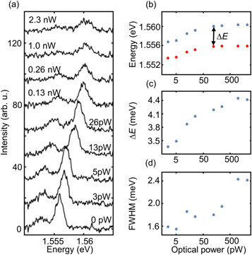
Figure 3. (a) Evolution of FEP and SEP for increasing laser powers of an additional over-barrier (HeNe) laser, while the sample is quasi-resonantly excited at 1.597 eV with a power of 450 nW. The power of the over-barrier laser varies between 0 pW and 2.3 nW (bottom to top). The trap (guard) gate is biased at VT = −0.2 V (VG = 0.0 V). (b) Fitted emission energies of both peaks as a function of optical power of the over-barrier laser. (c) and (d): corresponding energy splitting between both peaks and FWHM of the FEP as a function of the power of the over-barrier laser.
Download figure:
Standard image High-resolution imageWe now focus on the energy difference between FEP and SEP. In the picture of trions, it is established, that this splitting can be seen as the sum of the trion binding energy ETB and a term proportional to the local quasi-Fermi energy EF [42, 63]:

The relation (1) originates from the fact that in the process of the optical recombination of a trion, only one electron and one hole can recombine by photon emission, while the remaining charge carrier of the former trion-state has to be excited to a state above the the local Fermi energy. One would intuitively expect that aT should equal to 1 at zero temperature, however, different values aT > 1 have been reported e.g. for monolayer MoS2 [63]. In the limit of vanishing Fermi energy, the splitting is given by the bare trion binding energy. Yet, the experimental measurement of this binding energy can be complicated because a trion can also form bound complexes with charged impurity states in the barrier material [64, 65]. In our study, we observe the smallest FEP–SEP splitting ΔΕ in the center of the trap electrodes (e.g. figure 2(c) upper panel) to be less than ΔEmin = 0.4 meV. Thus, this value for ΔEmin serves as an upper bound of the bare trion binding energy in our heterostructure, and it is significantly smaller than the reported trion binding energies in broad single quantum wells [65]. We observe an apparent maximum of the SEP–FEP splitting in the order of ΔEmax ∼ 4 meV at the trap-edges (compare figure 3(c)). Taking relation (1), we partially attribute this value to the presence of a quasi-Fermi level of excess holes. We expect that additional interaction and renormalization effects play a role, which might result in a deviation from unity for the parameter aT [63]. Moreover, we find that the proximity to the trap-edge is the main factor which drives the emergence of the SEP (see figure 2). In this trion-picture, the exact densities of holes, IXs and trions might be difficult to determine. Nevertheless, we demonstrate in the next section that the interplay of the excitons with excess charge carriers has drastic consequences on the emission lifetime.
5. Lifetime measurements
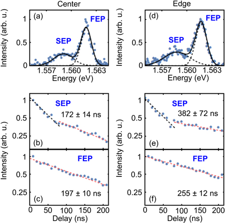
In order to verify the influence of the observed charge imbalance on the excitonic recombination dynamics, we measure the time-resolved photoluminescence of the exciton traps (without co-illumination). We excite the exciton ensembles with a 500 ns long, quasi-resonant laser pulse, and then integrate the photoluminescence in temporal windows of 10 ns for an increasing time-delay after the excitation. We utilize a laser repetition frequency of 80 kHz, because the corresponding long time delay of 12.5 μs = 80–1 kHz−1 allows for a complete recombination of the IX population between consecutive laser pulses. Figures 4(a) and (b) show exemplary normalized photoluminescence spectra recorded 140 ns after the laser pulse at the trap-center and trap-edge, respectively. In both cases, we find that the FEP and SEP are separated by ΔE ≈ 2.7 meV, which demonstrates that the time-resolved scheme allows accessing a trap configuration being consistent with figure 2(a) with mobile excitons and free charge carriers all over the trap. Moreover, we set VT = VG to allow for a comparable overlap of the electron- and hole-wavefunctions in the z-direction both at the trap-center and the trap-edge [66].
Figure 4. (a) Normalized photoluminescence spectrum taken at the center of the trap electrode after a pulsed (resonant) excitation. The excitation occurs at an energy of 1.597 eV with a pulse duration of a 500 ns and 1 μW optical power. The spectrum is taken 140 ns after the excitation pulse for a detection window of 10 ns. The peaks SEP and FEP are separated by 2.7 meV, as determined by Gaussian fits (black dashed lines). (b) Normalized temporal evolution of the area of the SEP in a logarithmic plot. We find two decay times of 72 ± 9 ns (black line) and 172 ± 14 ns (red line). (c) The decay of the FEP area can be fitted with only one characteristic lifetime of 197 ± 10 ns. Figures (d)–(f) present the similar data for a laser position at the edge of the trap electrode. Again, we find two lifetimes of 72 ± 14 ns (black line) and 382 ± 72 ns (red line) for the SEP decay (e) and one lifetime 255 ± 12 ns for the FEP. (f). Experimental parameters are f = 80 kHz, VT = VG = 0.0 V, Paverage = 25 μW, and TBath = 3 K.
Download figure:
Standard image High-resolution image
Figures 4(b) and (c) show the photoluminescence decay dynamics of both the FEP and SEP at the trap-center. We find that the SEP exhibits an initial fast decay with a time constant of 72 ± 9 ns (indicated by a black dashed line) followed by a second slower one with 172 ± 14 ns (red dashed line). The second lifetime is similar to the FEP lifetime with 197 ± 10 ns (bottom panel), which can be fitted by a single exponential decay. At the trap-edge, the fast (slow) SEP-lifetime time is 72 ± 14 ns (382 ± 72 ns) (figure 4(e)), and the FEP lifetime is slightly increased to be 255 ± 12 ns (figure 4(f)).
Intriguingly, a comparison of figures 4(a) and (d) shows that the energy of the FEP is very similar at the trap-center and trap-edge, yet the temporal dynamics are found to be considerably different (see figures 4(c) and (f)). We note that the findings are reproduced over a large set of parameters in time-correlated single photon counting experiments (with varying laser intensity and laser positions wrt. the traps), where we detect the spectrally integrated photoluminescence signal of both FEP and SEP with an avalanche photodiode. Most notably, the increase of the photoluminescence lifetime of the FEP towards the trap-edges complicates the understanding of the photoluminescence intensity enhancement at the trap-edges as in figure 2. In particular, a stronger photoluminescence signal at a constant excitation power and constant emission energy is usually attributed to a stronger oscillator strength and a faster radiative recombination. This single-particle argument is in contradiction to the findings in figures 4(c) and (f), as we discuss in the following.
6. Discussion
Since we observe the SEP only in the so-called trap configuration (i.e. VT < VG), we can deduce that the excess charge carriers in the CQWs are holes and in turn, that within the trion-picture, the SEP describes the photon emission from positively charged excitons [25, 35, 36]. Given the high electric field strength along the growth direction for the investigated range of VT and the relatively small tunneling barrier in-between the two quantum wells, we infer that both holes forming the trion complex are located in the same QW. Since the top electrode is negatively charged (VT < 0), both holes are located in the upper QW. The minimum energy separation of the FEP and SEP defines an upper limit of the bare binding energy to be 0.4 meV. Along this line, our results are in agreement with recent calculations by Witham et al, who suggest a binding energy of 0.22 meV for positively charged, unbound trions in a heterostructure with similar layer dimensions [67]. To compare, for bound trions, the binding energy is expected to be larger in the order of a few meV [68]. We conclude that the trions in the investigated CQWs are most likely unbound trions. We note, however, that at small excitation intensities, the in-plane propagation of IXs is limited by potential fluctuations (∼meV), which explains that the SEP shows spatial variations in figures 2(c) and (d). Figure 3 demonstrates that the energy splitting between the FEP and SEP can be tuned by co-illumination of the sample with an over-barrier excitation laser. We find a maximum energy splitting ΔEmax = 4.4 meV. Assuming relation (1) with aT ∼ 1 and ΔEmax = 4.4 meV [42, 63], we can estimate an apparent excess hole density of 3.3 × 1011 cm−2, for mh* ∼ 0.18 · m0. However, we note that mh* can vary in the range of (0.1–1) m0 [69, 70]. On first view, this apparent free hole density at the trap-edge is one order of magnitude higher than the expected IX density in our traps. However, we also performed a co-illumination measurement as shown in figure 3 in the trap-center, which shows a maximum energy splitting of ∼3 meV for 1 nW of the over-barrier excitation. The later power corresponds to only 0.3 mW cm−12 (note that the spot size of the HeNe laser is larger due to chromatic aberration of the optical elements), which is less than 1% of the resonant excitation power density. In this measurement at the trap-center, the Fermi energy contribution vanishes to zero (ΔE = 0) for minimal HeNe illumination, which is consistent with the findings in figures 2(c) and (d) without co-illumination. In other words, the initial IX ensemble in the trap-center is close to charge neutrality for low excitation powers. In turn, the exciton dissociation and drift dynamics at the trap-edge seem to play the essential role for the creation of charged exciton complexes in the overall trap. The FEPs remain significantly stronger than the SEPs for all excitation intensities, and only with increasing over-barrier pump, we observe a transfer of spectral weight from the FEP to the SEP. We therefore conclude that within the trion-picture, the local density of trions must be only a fraction of the IX density, and in turn, aT must be larger than one in our heterostructures. We further note that for the time-resolved spectra in the trap-center (see figure 4), the energy splitting ΔE between the FEP and SEP increases by 0.4 meV for delays 30 ns < Δt < 200 ns after the excitation pulse (data not shown). The increased splitting suggests that the ratio between excess charge carriers and neutral IX increases with time, and therefore, a certain fraction of excess charge carriers is not removed by radiative recombination of either IXs or trions.
Within the so-called polaron picture, the FEP (SEP) is the repulsive (attractive) polaron branch of the IX being dressed with the interaction with the excess charge carriers. The splitting of FEP and SEP as a function of excess charge carriers (see figure 3) is consistent with recent reports and a corresponding interpretation of exciton polarons in 2D materials, such as monolayer MoSe2 [50, 51]. Also in this picture, our data confirm the complex interaction between the photogenerated electron–hole pairs and the excess charge carrier density. We point out that our results are for indirect transitions as sketched by IX in figure 1(a). In such a double quantum well geometry, the specific recombination rates, the interaction strengths, and the dielectric screening are different compared to 2D materials [35]. We further note that the different interactions between the IXs and the excess charge carriers might be investigated by the help of a quantizing magnetic field, as recently reported for InGaAs-based double quantum wells with a modulation-doped excess electron density in the bottom quantum well [71]. In particular, we reported that integer and even fractional quantum Hall states in the excess electron system can give rise to non-trivial shifts in the emission energy of both DXs and IXs formed in such double quantum wells [71]. For the present laser-induced, non-equilibrium excess hole system, such experiments are beyond the scope of the present study, but first inelastic light scattering experiments point out a possible experimental route how to resolve the interactions with a much higher resolution than the presented photoluminescence experiments [35].
The obvious question is whether the finite photocurrent at the trap-edges (see figures 2(g)–(h)) stems from a photo-induced vertical leakage current or from an in-plane transport of excess charge carriers. The photocurrents are nominally measured with respect to the backgate of the field-effect structure, but the utilized indium-contacts are temperature-annealed from the top of the heterostructure to the backcontact. In other words, the indium contacts also penetrate the plane of the CQWs at a distance of several 10–100s μm away from the lithographically defined top gate electrodes. The CQW-heterostructures are of high quality, i.e. they are grown in an MBE-chamber where n-doped GaAs/GaAlAs-based heterostructures frequently achieve electron mobilities exceeding few 107 cm2 V−1 [72, 73]. In other words, photogenerated excess charge carriers which move away from the trap-edges can easily propagate for a lateral distance of hundreds of micrometer. That is typically the distance of the traps in our experiments to the indium contacts. In turn, we performed control experiments on etched circuits where the lateral area between the trap region and the indium contacts where etched down to about 250 nm. Such 'etched' trap circuits exhibit a photocurrent reduction of up to two orders of magnitude. Still, the 'etched' samples show a SEP at the edge of the trap electrode. This control experiment suggests that first, the trap-edges give rise to the dissociation of IXs, second, that the corresponding excess charge carriers can move in the plane of the CQWs for large distances, and third, that the photocurrent in the figures 2(e)–(g) is dominated by this in-plane motion. Consistently, the photocurrent for low excitation powers (as in figures 2(f) and (g)) is below 1 pA for excitation at the trap-centers.
The significance of the observations is manifest in the non-trivial dependence of the photoluminescence lifetimes of the FEP and SEP on the emission position, i.e. in the trap-center and at the trap-edge (figure 4). A straightforward single-particle model estimates the radiative lifetimes from the overlap of electron and hole wave functions in the z-direction [66]. The model suggests that the lifetime of the IXs should quadratically depend on the energy difference between direct and indirect excitons:

with tDX the lifetime of the direct excitons, which is typically in the order of ∼1 ns. We note that relation (2) can indeed be applied to the data of our experiments when the photoluminescence is measured at some positions in the trap-center. However, relation (2) is in striking contrast to the results presented in figure 4. In particular, figures 4(a) and (b) demonstrate that the FEP energy is almost identical in the center and at the trap-edge (EDX is constant in both cases). Still, the radiative lifetime of the FEP and SEP is significantly increased at the trap-edges. Generally, the observed three-fold increase in photoluminescence intensity at the trap-edges is consistent with recent reports on a charge imbalance in excitonic systems [41]. We further note that a charge imbalance in excitonic traps is often present—in particular, when an over-barrier laser excitation is utilized, but sometimes it is even wanted. For instance, in the reported macroscopic bright rings in heterostructures without any trap geometry [74], the rings are formed at the lateral boundary between electron- and hole-rich regions [75].
For observing a BEC of trapped IXs, such excess charge carriers constitute a certain challenge. A strategy to avoid the impact of excess unbound charge carrier is to utilize CQWs, which are individually charge-tunable by side-gates [76], such that the photogenerated excess charge carrier densities can be compensated by tunable background densities per quantum well. However, also there, as soon as an electrostatic trap is formed, the dissociation of excitons and a local imbalance of excess charge carriers occur at the trap-edges. A very similar situation of excess charge carriers occurs in the above mentioned bright exciton rings [77], where the different diffusivities of electrons and holes in III–V semiconductors create a charge imbalance in the center of such rings. We point out that the vertical tunneling is rather low in our heterostructure (compare figures 2(e)–(h)). We further verify this statement by observing that the photocurrents as in figure 2 are largely suppressed in 'etched' traps (see discussion above), while the SEPs still exist. One possibility seems to position the CQW close to the back-contact and to utilize a resonant excitation. Another possibility to overcome the problem of excess charge carriers at the trap-edges seems to be the use of many gates [32] where the interplay of all gates form the overall electrostatic traps in the direction of [78]. For two respective neighboring gates, the gate voltage needs to be small enough such that the IXs are not dissociated. At the same time, the lateral distance between two neighboring gates must be small enough to avoid the electrostatic impact of optically excited surface states [79]. However, it should be considered that for too small distances, the resulting Ex component easily exceeds the binding energy (see figure 1(c)). Last but not least, the macroscopic scale of such a multi-gate trap configurations must be large enough such that the absolute number of IXs is sufficient for a many-body condensation process and substantial condensate fraction, while keeping the density in the dilute limit [80, 81].
7. Summary
To conclude, we find that the apparent parabolicity of excitonic trap potentials is connected to the charge imbalance in the IX ensembles, and that this imbalance exhibits a pronounced increase towards the trap-edges. The presence of excess charge carriers results in the emission of a second luminescence peak below the emission which is typically referred to as the neutral IX. Surprisingly, the charge imbalance at the trap-edges coincides with an increased radiative lifetime of the photoluminescence at these positions and an increased photoluminescence intensity. These combined findings do not allow for straight-forward explanations in terms of altered wave function overlap of electron and hole states, light cone population or changed IX density. Our results are particularly relevant for the interpretation of IX photoluminescence with respect to possible condensation into a dark condensate [82].
Acknowledgments
We acknowledge financial support of the Deutsche Forschungsgemeinschaft (DFG) via the excellence cluster 'Nanosystems Initiative Munich' (NIM) and projects HO3324/9-1 and WU 637/4-1. Research at Purdue was supported by the US Department of Energy, Office of Basic Energy Sciences, Division of Materials Science and Engineering under award DE-SC0006671.