
Abstract
Although we can use misorientation angle to distinguish the grain boundaries that can carry high critical current density  in high temperature superconductors (HTS) from those that cannot, there is no established normal state property equivalent. In this paper, we explore the superconducting and normal state properties of the grains and grain boundaries of polycrystalline YBa2Cu3O7−x (YBCO) using complementary magnetisation and transport measurements, and calculate how resistive grain boundaries must be to limit
  in polycrystalline superconductors. The average resistivity of the grain boundaries,
  in our micro- and nanocrystalline YBCO are 0.12 Ωm and 8.2 Ωm, values which are much higher than that of the grains
  and leads to huge
  values of 2 × 10³ and 1.6 × 10⁵ respectively. We find that the grain boundaries in our polycrystalline YBCO are sufficiently resistive that we can expect the transport
  to be several tens of orders of magnitude below the potential current density of the grains in our YBCO samples, as is found experimentally. Calculations presented show that increasing
  values by ∼2 orders of magnitude in high fields is still possible in all state-of-the-art technological high-field superconductors. We conclude: grain boundary engineering is unlikely to improve
  sufficiently in randomly aligned polycrystalline YBCO, to make it technologically useful for high-field applications; in low temperature superconducting intermetallics, such as Nb3Sn, large increases in
  may be achieved by completely removing the grain boundaries from these materials and, as is the case for thin films of Nb, Ba(FeCo)2As2 and HTS materials, by incorporating additional artificial pinning.
Export citation and abstract BibTeX RIS

Original content from this work may be used under the terms of the Creative Commons Attribution 3.0 licence. Any further distribution of this work must maintain attribution to the author(s) and the title of the work, journal citation and DOI.
1. Introduction
The applied superconductivity research community is always trying to increase the critical current density  of superconducting materials. There are two quite distinct requirements for achieving high
  in practical materials. The local depairing current density
  which is the theoretical limit associated with the density of Cooper pairs, must be high enough throughout the entire material, and the current density associated with local flux pinning
  must be sufficiently high to stop flux motion. Thereafter many other issues, such as the strain and/or irradiation tolerance of
  or the thermal stability of the conductor, become important depending on the application. But, in most applications, high
  in high magnetic fields is usually the primary technological and economic driver.
In the historical development of the low temperature superconductor (LTS) Nb3Sn, reducing the grain size in polycrystalline material, significantly increased  in high magnetic fields [1]. It was reasonable to assume that in such an intermetallic superconductor, smaller grain size increased pinning and that the metallic bonding ensured that
  was sufficiently high throughout the entire material that any depression in
  in the grain boundaries was unimportant. However, over the last decade the progress in increasing
  in Nb3Sn has been relatively slow and the simple pinning approach that considers flux pinning alone (e.g. fluxons depinning themselves from isolated pinning sites) has not helped produced any further significant increases in
  More recent computational three-dimensional time-dependent-Ginzburg–Landau (TDGL) modelling [2] has shown that in polycrystalline superconductors, the dissipation mechanism can consist of fluxons moving along grain boundary channels past fluxons that are held stationary within the grains by strong surface pinning. The increase in pinning due to smaller grains is most likely caused by an increase in the density of triple points along the channels or by providing a more tortuous channel path along which the fluxons must flow. Hence, we suggest that in polycrystalline materials, it is useful to consider depairing and depinning separately and invoke separate values of
  and
and  for both the grains and the grain boundary channels. This approach helps articulate the open question of whether further significant increases in
  will be achieved, even in LTS polycrystalline materials, by increasing
  or by increasing
  along grain boundary channels. Since in practice we cannot completely decouple
  and
and  and
and  cannot be larger than
  this approach becomes one of identifying whether or not
  is sufficiently low (at the grain boundaries), that it is the barrier to achieving further increases in
In developing high temperature superconductors (HTS), the role of grain boundaries was found to be quite different to that of LTS [3, 4]. In the pioneering work of Dimos et al [3],  was measured in YBa2Cu3O7−x (YBCO) bicrystals for different geometries and was found to decrease exponentially with increasing misorientation angle. This led to research into repairing the grain boundaries such as doping them to improve oxygen content or carrier concentration, with a view to increasing
  [5, 6]. Experimental work was also supported by computational studies which included modelling the flow of current through a grain boundary at an atomic level [7] and modelling grain boundaries, both analytically [8] and using TDGL theory [2, 9, 10]. Eventually, industry concluded that large-angle grain boundaries in HTS materials depressed
  so severely that it committed itself to making kilometre-length pseudo single-crystal 2 G tapes of HTS [11] that were designed to completely exclude large-angle grain boundaries. In parallel with the development of 2 G tapes, the language of 'weak-links' was developed in the literature. It emphasised that although some materials have local regions of very high
  the practical limit for a material is usually determined by those regions of lowest
  although it does not make clear whether the 'weak-link' is because of low
  or low
Understanding and improving grain boundaries in both LTS and HTS materials is important because despite the huge applied superconductivity research effort,  in most materials is still far from its maximum theoretical value—the depairing current density of the superconductor
  [12]. The first panel in figure 1 shows the critical current density versus field at 4.2 K in the superconducting layer of many of the most important high-field superconductors. There are other similar datasets in the literature, such as the excellent webpage produced and maintained by Lee [13]. Samples reported in figure 1 were chosen by prioritising datasets providing a broad range of magnetic field data, and the quality of samples and measurements. The second panel in figure 1 shows the data replotted as current density normalised by the depairing current density at zero field and 4.2 K
  versus the applied magnetic field normalised by the upper critical field at 4.2 K
  The temperature-dependent depairing current density in zero field has been calculated using

where for isotropic materials,  is the flux quantum,
  is the Ginzburg–Landau (G–L) penetration depth and
  is the G–L coherence length. The
  curve shows the in-field theoretical limit derived from G–L theory where
  where
where 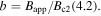 The appendix provides the method used for calculating the depairing current density in anisotropic materials and table 1 lists the values of
  used to produce the second panel [13–25]. We note that for YBCO, Ba(FeCo)2As2 and FeSe0.5Te0.5, there are small differences in the values of
  and
and  due to the fact that
  and
and  (or
(or  ) were measured by different groups on different samples. We have neglected the differences between the upper critical field and the irreversibility field, which are generally only important at high temperatures for the HTSs (typically when the
  values are low) [26–28]. The second panel in figure 1 shows that even in technologically mature materials such as NbTi,
  values in high magnetic fields are still nearly two orders of magnitude below the theoretical upper limit of the depairing current density. The third panel in figure 1 shows
  normalised to unity at 0.2
 One can globally fit these normalised data using the long-established standard flux pinning equation, of the form

where  and
and  The values of
  and
and  vary considerably from one material to another when fitted individually. For example for NbTi,
  and
and  whereas for the A15 compounds,
  and
and  [29]. Nevertheless, the panel shows that to first order, the in-field behaviour of
  is not very different across this range of quite different superconducting materials. Equally the data are reasonably well parameterised by an equation used for high temperature superconducting materials of the form [8, 30]

where at  = 4.2 K,
  and
and  Equation (2) suggests flux pinning is important whereas the exponential in equation (3) suggests the decay of the order parameter across the grain boundaries is important. Hence, although the physical processes associated with these two equations are completely different, it is clear that fitting the data to one or other field dependence does not provide evidence for, or distinguish between, which mechanism operates [31].
Figure 1. Upper panel: critical current density of the superconducting layer  as a function of applied magnetic field
  The
The  data for YBCO (Superpower 'Turbo' double layer tape), Bi-2212 (OST 2212 wire with 100 bar over-pressure) and Bi-2223 (Sumitomo Electric Industries 'DI' BSCCO tape) are taken from [28].
  data for Nb (thin film with artificial nanoscale pores) [12] (measured at 5 K), Nb–47Ti ([133], 37% superconductor cross-section area (SCSA)), Nb3Sn (Internal Sn RRP (IT), 12% SCSA [96] and High Sn Bronze-route (B), 11% SCSA [97]), Nb3Al (jelly-roll strands, 32% SCSA) [116], (NbTa)3Sn (11% SCSA) [117], PbMo6S8 [134], MgB2 (AIMI 18 Filament (39% Filament CS)) [94], FeSe0.5Te0.5 (thin film IBAD substrates) [95] and Ba(FeCo)2As2 (thin film on CaF2 substrates) [91] are also included. Closed and open symbols are used for anisotropic materials and signify that the magnetic field is parallel and perpendicular to the ab-plane respectively. Middle panel:
  normalised by the superconducting depairing current density
  (0 T, 4.2 K) as a function of normalised field
  (4.2 K) for the same materials as the upper panel. Values of
  (0 T, 4.2 K) were calculated using the method outlined in the appendix. In anisotropic materials, the
  (0 T, 4.2 K) associated with the direction of current flow (i.e.
  (0 T, 4.2 K)) were used. Lower panel:
  normalised by its value at the
  (4.2 K) as a function of normalised field
  (4.2 K) for the same materials as the upper panels. The solid red curve was fitted using equation (2), with
  and
and  and the dashed black curve was fitted using equation (3) with
  and
and  The fitting parameters were obtained without considering MgB2.
Download figure:
Standard image High-resolution imageTable 1.
The depairing current density at zero magnetic field and 4.2 K,  (0 T, 4.2 K), and the parameters used to calculate it for important high-field superconductors.
  is the critical temperature,
  is the exponent derived from the empirical equation
  The upper and lower critical fields
  and
and  are given at 0 K and given for the magnetic field applied parallel to the ab-plane and parallel to the c-axis. For anisotropic materials, the G–L coherence length and G–L penetration depth are given parallel to the ab-plane, the c-axis as well as an angular average at 0 K. Anisotropic material parameters are taken from single crystals. Parameters for high-field isotropic superconductors were taken from wires. Parameters that were obtained from temperature-dependent experiments in the literature have the relevant reference cited next to them. Calculated parameters are labelled with an uppercase star: *. For Nb†: critical values are at 5 K and
  were estimated from extrapolating critical current data to zero [12]. For (NbTa)3Sn†:
  was taken to be the same as Nb3Sn. For Bi2Sr2Ca2Cu3O10†:
  was taken to be the same as Bi2Sr2CaCu2O8; The value of
  is small, determined from high temperature data.
| Material |
 (K) (K) |

|
 (T) (T) |
 (mT) (mT) |
 (nm) (nm) |
 (nm) (nm) |
 (0, 4.2) (1012 Am−2) (0, 4.2) (1012 Am−2) |
|
|---|---|---|---|---|---|---|---|---|
| Nb (5 K) | 7.50 [12] | 1.4 [114] | 2.61† | 34.3* | 9.67* | 79.0† [14] | 0.322* | |
| NbTi | 8.99 [15] | 1.8 [15] | 15.7 [15] | 13.5* | 3.40* | 163 [14] | 0.434* | |
| PbMo6S8 | 13.7 [115] | 1.7 [115] | 56.0 [115] | 6.40 [115] | 1.89* | 265* | 0.441* | |
| Nb3Al | 15.6 [116] | 1.3 [116] | 26.5 [116] | 68.7* | 3.15* | 65.0 [52] | 4.74* | |
| (NbTa)3Sn | 16.8 [117] | 1.1 [117] | 32.0 [117] | 38.0† | 3.06* | 91.9* | 2.53* | |
| Nb3Sn | 17.8 [118] | 1.5 [31] | 29.5 [118] | 38.0 [119] | 2.73* | 93.5* | 2.83* | |
| MgB2 | 38.6 [120] | ab: | 0.75 [120] | 25.5 [120] | 38.4 [120] | 7.07* | 97.1* | 1.27* |
| c: | 0.72 [120] | 9.20 [120] | 27.2 [120] | 2.44* | 282* | 0.439* | ||
| 〈 〉: | 3.74* | 129* | 0.980* | |||||
| Ba(FeCo)2As2 | 25.8 [121] | ab: | 1.8 [121] | 64.7 [121] | 4.76* | 2.18* | 350 [122] | 0.289* |
| c: | 1.2 [121] | 56.4 [121] | 3.75* | 1.26* | 605* | 0.167* | ||
| 〈 〉: | 1.86* | 413* | 0.246* | |||||
| FeSe0.5Te0.5 | 14.0 [123] | ab: | 3.0 [123] | 44.0 [123] | 2.00 [124] | 2.16* | 317* | 0.272* |
| c: | 1.5 [123] | 47.0 [123] | 4.50 [124] | 1.15* | 593* | 0.145* | ||
| 〈 〉: | 1.80* | 381* | 0.228* | |||||
| YBa2Cu3O7-x | 90.0 [20] | ab: | 2.7 [20] | 250 [20] | 9.15* | 1.29* | 135 [19] | 4.00* |
| c: | 1.7 [20] | 120 [20] | 23.3* | 0.378* | 894 [19] | 0.604* | ||
| 〈 〉: | 0.969* | 208* | 2.65* | |||||
| Bi2Sr2CaCu2O8 | 84.8 [125] | ab: | 3.24* | 300 [125] | 0.321* | |||
| c: | 0.14 [26] | 231 [26] | 4.60* | |||||
| 〈 〉: | ||||||||
| Bi2Sr2Ca2Cu3O10 | 108 [23] | ab: | 2.86* | 165 [126] | 1.22* | |||
| c: | 0.14† | 297 [23] | 13.8* | |||||
| 〈 〉: | ||||||||
It is long-known that wide, insulating grain boundaries prevent supercurrent crossing them. In this paper, we provide a quantitative description of when grain boundaries can be considered sufficiently resistive to limit  using our data on both microcrystalline and nanocrystalline YBCO. We have chosen these materials because: their fundamental properties in single crystal form are well known; the polycrystalline materials presented here provide a huge range of superconducting transport properties; and there is a huge commercial potential if cheap polycrystalline HTS materials can be fabricated with high
  In addition, our group has developed the expertise to make good nanocrystalline materials [32–37]. The approach we have adopted is to try to make a sufficiently broad range of YBCO samples and measurements to enable us to identify whether
  or
or  limits
  The structure of this paper is as follows: section 2 of this paper describes the sample fabrication process and the microstructure of the materials studied. The results from the transport and magnetic measurements used to characterise the samples are shown in section 3. Section 4 provides the theoretical considerations we have used to analyse our data and that of the literature. In section 5, we discuss our YBCO data and consider other high-field superconductors, in particular Nb3Sn. Finally, the conclusions are summarised in section 6.
2. Fabrication of nanocrystalline materials
2.1. Sample milling and HIP'ing
Samples with two different compositions were made for this work—Y1: YBa2Cu3O7−x and Y2: 75 wt% YBa2Cu3O7−x + 25 wt% Y2BaCuO5 to which an additional 1 wt% CeO2 was added [38, 39]. Commercial YBa2Cu3O7−x, Y2BaCuO5 (99.98%, Toshima) and CeO2 powders (99.99%, Alfa Aesar) were used to fabricate the samples. The Y1 samples were produced from the commercial powders directly. The Y2 composition was chosen because of its high  in bulk single crystal form [40]. Powders were first mixed together by shaking the starting powders for 30 min in a stainless steel vial using a SPEX 8000D high-energy shaker mill. Next, samples were milled using the miller and tungsten carbide (WC 94/Co 6) milling media in an argon atmosphere. In an earlier pilot study, we used copper milling media [35]. Although it is expected that copper is less detrimental to the superconducting properties of YBCO than WC or Co, we choose not to use Cu milling media in this work because it is too soft. The samples were milled in batches of 10 g, with a ball-to-powder mass ratio of 3:1, for a total of 30 h. The milling vial and balls were scraped with a tungsten carbide rod regularly, in argon, to increase yield and improve homogeneity. The powders were placed into small niobium foil packets (0.025 mm thick, 99.8%, Alfa Aesar), which acted as a diffusion barrier and then consolidated using a hot isostatic press (HIP). The Nb packets were sealed into stainless steel tubes (type 316, 1 mm thickness) and HIP'ed at a temperature of 400 °C and pressure of 2000 atm for 5 h. Many samples were subsequently annealed in pure flowing oxygen atmosphere in a dedicated oxygen furnace to optimise oxygen content and restore some crystallinity. In this paper, the letters 'P', 'M', 'H' and 'A' denote that a sample has been processed through a combination of powder or pellet Pressing, Milling, HIP'ing, or Annealing respectively. The letters are added after the label for composition in the order that they occurred during processing. Table 2 lists the microcrystalline and nanocrystalline samples where the superconducting properties have been studied in detail.
Table 2.
The fabrication process, transport and magnetic properties of the microcrystalline and nanocrystalline samples in this paper. 'Y1' and 'Y2' represent Y123 and Y123 + Y211 + CeO2 compositions respectively. The letters 'P', 'M', 'H', and 'A' stand for pressed powders, milled, HIP'ed and annealed respectively. Milled samples (M) were milled for 30 h. HIP processing (H) was at 400 °C and 2000 atm for 5 h. Letter 'A' denotes the standard annealing heat treatment used, which includes a dwell at 750 °C for 20 h followed by 450 °C for 60 h. Ramping between temperatures was completed at 600 °C h–1. A* denotes using heat treatment A, but with a ramp rate of 60 °C h–1. B denotes a dwell at 450 °C for 20 h, followed by heat treatment A. A × 2 and A × 3 were heat treated using heat treatment A, twice and three times respectively.  was determined from the onset of ACMS data. 'Para' indicates a sample behaves paramagnetically and that no
  was measured.
  was determined by extrapolation from variable temperature susceptibility data (figure 13) and equation (8). μ0ΔM/ΔB is from d.c. magnetisation hysteresis measurements.
  is the magnetisation critical current density at zero field and 4.2 K unless otherwise stated, calculated using the grain dimensions of the samples.
  is the transport critical current density at a 1 mV m–1 criterion.
  (300 K) is the normal state resistivity at 300 K. The symbol '—' denotes that the property was not measured.
| Sample | Grain size (nm) | Annealed |
 (K) (K) |
 (T) (T) |

|
 (A m–2) (A m–2) |
 (A m−2) (A m−2) |
 (300 K) (Ω m) (300 K) (Ω m) |
|---|---|---|---|---|---|---|---|---|
| Y1P | 5000 | — | 81 | 140 | −2 × 10⁻¹ | 8.3 × 10¹⁰ | — | — |
| Y1H | 5000 | — | 53 | 70 | −3 × 10⁻² | 4.1 × 10¹⁰ | — | — |
| Y1HA | 5000 | A | 86 | 163 | −2 × 10⁻¹ | 2.9 × 10¹¹ | 1.2 × 10⁵ (0.1 T, 4.2 K ) | 7.1 × 10⁻⁵ |
| Y1MH | 20 | — | Para | — | — | — | — | 62 |
| Y1MHA(1) | 100 | A | Para | — | −4 × 10⁻⁴ | 9.3 × 10⁹ | Resistive | 2.5 × 10⁻² |
| Y1MHA(2) | 100 | A* | Para | — | −6 × 10⁻⁴ | 1.0 × 10¹⁰ (10 K) | Resistive | 2.0 × 10⁻² |
| Y1MHA(3) | 100 | B | 70 | 66 | −3 × 10⁻³ | 4.5 × 10¹⁰ | Resistive | 8.9 × 10⁻³ |
| Y1MPA | 25 | A | 73 | 40 | −2 × 10⁻³ | 2.7 × 10¹⁰ | — | — |
| Y2P | 5000 | — | 81 | 119 | −1 × 10⁻¹ | 5.1 × 10¹⁰ | — | — |
| Y2H | 5000 | — | 53 | 62 | −2 × 10⁻² | 4.0 × 10¹⁰ | — | — |
| Y2HA | 5000 | A | 83 | 132 | −2 × 10⁻¹ | 1.5 × 10¹¹ | — | — |
| Y2MHA(1) | 100 | A | Para | — | — | — | — | 1.0 × 10⁻² |
| Y2MHA(2) | 100 | A × 2 | Para | — | −7 × 10⁻⁴ | 1.7 × 10¹⁰ (10 K) | 70 (0 T, 2 K) | 5.2 × 10⁻³ |
| Y2MHA(3) | 100 | A × 3 | 17 | — | — | — | — | — |
2.2. X-ray diffraction (XRD) and SEM
The phases present and grain sizes of the samples were obtained using powder XRD measurements. Figure 2 shows the evolution of the XRD spectra for the as-supplied powders with the compositions Y1 and Y2, after they were milled for up to 30 h. Both compositions show similar behaviour, namely the peaks broadened with increased milling time. The associated decrease in the grain size of the YBa2Cu3O7−x was calculated using TOPAS Academic software and Rietveld refinement. The insets show the grain size as a function of milling time. The grain size of the as-supplied materials is estimated to be 5 μm from SEM (not shown). Within the first 5 h of milling, the grain size is drastically reduced by 3 orders of magnitude down to the nanometre scale. After 30 h, the reduction in grain size saturates as it reaches <10 nm. Figure 3 shows the XRD spectra of the MP, MH and MHA samples. The additional peaks at 30° in the Y1MHA(1) 30 h milled sample and at 24° in the Y2MHA(1) 30 h milled sample should be interpreted with care. We attribute these peaks predominantly to our samples being ground in air for and prior to XRD measurement itself, and the known high sensitivity of YBa2Cu3O7−x to decomposition to parent oxides and Y2BaCuO5 in the presence of water vapour in air, particularly in highly milled samples [41–43]. We do not expect such decomposition to occur in our bulk HIP'ed samples that were not exposed to air. We have not identified the peak at 29° in the Y2MHA(1) sample. The grain size of the MHA samples is approximately 100 nm, with a relatively large uncertainty of a factor of 2, due to the unidentified peaks and high strain in these materials that complicates the refinement process. Trace amounts of WC were found in the XRD and EDX (not reported here) in some milled materials of both Y1 and Y2 compositions. There exist methods in which the oxygen content of YBa2Cu3O7−x can be calculated using an analysis of the c-axis lattice parameter, however we were unable to apply such analysis to our samples because of the very high strain content in these milled materials [44].

Figure 2. X-ray diffraction patterns for the composition Y1 (upper panel) and the composition Y2 (lower panel) after milling for up to 30 h. Inset: grain size as a function of milling time. The 5 μm data point in the as-supplied material (at 0 h) is obtained from scanning electron microscopy.
Download figure:
Standard image High-resolution image
Figure 3. Upper panel: x-ray diffraction patterns for Y1P, Y1MP, Y1MH and Y1MHA(1). The main YBa2Cu3O7−x peaks are labelled. Lower panel: x-ray diffraction patterns for Y2P, Y2MP, Y2MH and Y2MHA(1). In addition to the YBa2Cu3O7−x peaks labelled in the upper panel, the main Y2BaCuO5 peaks are labelled in the lower panel.
Download figure:
Standard image High-resolution image2.3. Thermal gravimetry (TG)/differential scanning calorimetry (DSC)
Figure 4 shows the TG and DSC data for the P, MP and MHA samples for both Y1 and Y2 compositions. Data were obtained over two cycles. In each cycle, samples were heated up to 1100 °C and cooled back to room temperature in a pure argon atmosphere at 10 °C min−1. As was the case for the XRD data, one has to be careful interpreting the data for the highly milled samples. Although the DSC/TG samples were not powdered, they were exposed to air when they were transferred into the DSC/TG sample-holder cups prior to measurement. In particular, any significant mass loss or DSC peaks below 200 °C are usually associated with moisture.

Figure 4. Differential scanning calorimetric signal and thermogravimetric signal (showing percentage mass change) for Y1P, Y1MP, Y1MHA(1), Y2P, Y2MP, Y2MHA(1) samples between 100 °C and 1100 °C, at 10 °C min−1. Upper panel: the heating part of the first cycle. Lower panel: the heating part of the second cycle. Significant endothermic peaks, associated with melting are labelled with • symbols and exothermic peaks, associated with the crystallisation of amorphous and recrystallisation of nanocrystalline phases, by the ♦ symbol.
Download figure:
Standard image High-resolution imageBoth TG and DSC data for the (as-supplied) Y1P and Y2P samples are in broad agreement with equivalent data from the literature [35]. The mass losses between 400 °C and 800 °C are consistent with oxygen loss of YBa2Cu3O7−x phase from O7 to O6 and there are large endothermic melting peaks with onsets at 970 °C [35]. The Y1P, Y1MP and Y2P samples were most stable to mass loss during both cycles. The other three samples showed mass loss over the entire temperature range during both cycles. The only clear exothermic peaks were observed at about 630 °C as indicated by the ♦ symbols for the Y1MP and Y2MP milled samples in the first cycle. We associate these peaks at ∼630 °C with crystallisation of amorphous, and recrystallisation of nanocrystalline phases, to produce larger grain sizes [45]. As expected, such peaks were not present in unmilled samples Y1P or Y2P nor in any of the second cycle data for any of the samples. These results led us to choose a HIP temperature of 400 °C to fabricate the YBCO materials in this work, to prevent excessive grain growth and follow an approach we have successfully used before to make other nanocrystalline materials [32–37]. In the two samples that were milled, HIP'ed, and annealed (Y1MHA(1) and Y2MHA(1)), there was increased and significant mass loss near 850 °C in cycle 1 and coincident large endothermic peaks, both of which are absent in cycle 2. We attribute these peaks to melting and oxygen loss. At the highest temperatures of the cycles, we associate the large endothermic melting peaks in figure 4 as follows: the peaks that occur in both panels near 1000 °C are due to melting of the YBa2Cu3O7−x phase—the exact melting temperature is dependent on oxygen content [46] and expected to be lower in argon atmosphere than in air [47]. The peaks with an onset near 993 °C are due to the reactions Y2BaCuO5 + BaCuO2 → Liquid and YBa2Cu3O7−x +BaCuO2 → Y2BaCuO5 + Liquid [48]. The peaks with an onset near 875 °C are due to the reaction YBa2Cu3O7−x +BaCuO2 + CuO → Liquid [48]; and the peaks near 839 °C to melting of BaCuO2 phase [35].
3. Experimental results and analysis
3.1. Transport measurements—resistivity and critical current density
HIP'ed samples were shaped into cuboid bars for transport measurements with typical dimensions of 1 × 1 × 5 mm. The samples were mounted onto a physical property measurement system (PPMS) resistivity puck [49]. Current and voltage leads were connected to the sample using silver paint for standard four-terminal measurements. The voltage taps were typically 2.5 mm apart. Control and measurement of the temperature and the magnetic field were made using the PPMS. To measure  traces, the puck was connected to external high-precision voltmeter and current sources. The current was supplied by a Keithley 220 programmable current source. A resistor was added in series to the sample in order to confirm that the current through the sample was equal to the nominal output current in the range of 10 nA–0.1 A. The voltage across the sample taps was measured with a Keithley 2100 6½ digit multimeter, with an additional ×50 000 amplifier [50] when required, to measure extremely small voltages. Figure 5 shows a summary of the resistivity data for the samples in this paper as a function of temperature, measured using excitation currents of typically 5 mA.

Figure 5. Resistivity as a function of temperature for all the materials of Y1-composition and the Y2MHA(1) and Y2MHA(2) samples. The strong effect of oxygen annealing can be seen in both micro and nanocrystalline materials, decreasing  by a factor of ∼102 and 103 respectively. However only three nanocrystalline materials showed a superconducting transition: Y1MHA(3), Y2MHA(1) and Y2MHA(2). Single crystal literature data were taken from [81].
Download figure:
Standard image High-resolution imageThe YBCO microcrystalline sample that was simply HIP'ed (Y1H) has a weak temperature-dependent resistivity with no evidence of superconductivity. Oxygen annealing decreased  by more than a factor of 103 and a superconducting transition was observed, which can be seen in the in-field data in the upper panel of figure 6 for sample Y1HA. In zero magnetic field, the onset
  is 92 K and zero-resistivity occurs at 60 K. Figure 6 shows that as the applied field was increased, the onset
  that we associate with the grains, does not vary significantly, whereas the zero-resistivity
  likely associated with the grain boundaries, is very significantly decreased. These findings are consistent with those of Dimos et al [51] where the largest suppression of superconductivity in relatively small fields occurs at the grain boundaries. The lower panel compares the values of
  for Y1HA to those of single crystals in which current flows either along the c-axis direction or along the ab-plane. Figure 7 shows the equivalent
  traces for Y1HA. The
  traces show superconductivity between 0 and 8 T at 4.2 K. Zero field
  data were also obtained up to 120 K in steps of 10 K, and thereafter up to 300 K in steps 50 K. Using a 1 mVm–1 criterion, the transport
  is 1.2 × 10⁵ Am–2 at 0.1 T and 4.2 K. Figure 8 shows the transport
  of Y1HA determined using the same criterion. The inset includes the zero field
  from 40 and 60 K. As shown later in section 3.3, the intragranular magnetisation
  in this sample is of the order of 1011 Am–2. Hence the transport
  values measured here are six orders of magnitude lower than the intragranular currents.

Figure 6. Upper panel: resistivity of Y1HA sample measured in fields of 0–8 T with a constant excitation current of 5 mA. Inset: detail of the two-step transition. Lower panel: resistivity of Y1HA in zero field compared to the resistivity of a single crystal of YBCO along the c-axis  and along the ab-planes
  [81] and the angular averaged resistivity
  calculated using equation (16).
Download figure:
Standard image High-resolution image
Figure 7. Upper: voltage as a function of current  of Y1HA sample at 4.2 K and various magnetic fields. The dashed lines show the electric field criteria of 1 mV m−1 and 100 μV m−1. Lower:
  data from 40 to 70 K at zero field.
Download figure:
Standard image High-resolution image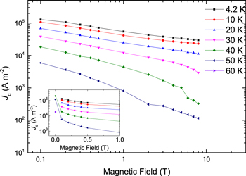
Figure 8. Transport  of Y1HA as a function of field and temperature using 1 mV m−1 criterion from 4.2 to 60 K. The inset shows the zero-field data obtained.
Download figure:
Standard image High-resolution imageAs can be seen in figure 5, the nanocrystalline materials have resistivity values typically three or four orders of magnitude higher than microcrystalline materials. Y1MH sample has the highest  of all the samples—60 Ωm at 300 K. For comparison, the values of the resistivity of a good metal like Cu and a good insulator like diamond are 10–8 Ωm and 1010–1011 Ωm [52]. After annealing, the resistivity decreased by a factor of approximately 103 at room temperature. A smaller, further reduction was found by repeating the annealing process as in the case for Y2MHA(1) and Y2MHA (2). The
  traces of nanocrystalline Y1MHA(1), (2) and (3) were entirely resistive with no signs of percolating supercurrents. Y1MHA(3) shows an inflection in
  at 60 K which can also be seen in ac magnetisation discussed in section 3.2. We tried many different annealing procedures to produce supercurrents flowing across grain boundaries. A single nanocrystalline sample showed evidence that it could transport an intergranular supercurrent. Figure 9 shows the in-field resistivity of nanocrystalline materials of the Y2 composition. This sample was annealed twice. The data after the first annealing, Y2MHA(1), is given by solid symbols, and the data after the second annealing, Y2MHA(2), is given by the open symbols. The second annealing decreased the resistivity by at least a factor of 2 over the entire temperature range. The inset shows the
  trace of the sample after the second annealing, measured at 2 K and 0 T. It provides evidence for very weak superconductivity. The transport
  at 2 K and 0 T was very small, equivalent to about 70 Am−2 at an electric field criterion of 1 mV m–1. This is at least 109 times lower than the transport
  of commercial YBCO tapes.

Figure 9. The resistivity of the Y2MHA(1) sample (solid symbols) as a function of temperature in fields of up to 8 T (measured with an excitation current of 10 μA). At zero field, the peak resistivity is at 52 K and the resistivity does not reach zero at 2 K. The Y2MHA(2) data at zero field is the open squares. The resistivity has decreased at all temperatures and the temperature at which peak resistivity has increased to 64 K. Inset: voltage as a function of current of Y2MHA(2) at 2 K and 0 T, showing evidence for very weak superconductivity.
Download figure:
Standard image High-resolution image3.2. AC magnetic susceptibility
The ac magnetic susceptibility and dc magnetisation measurements were all taken in our Quantum Design PPMS system [53]. The non-HIP'ed samples were pressed into pellets with a typical size of 3 mm diameter and a height of 2 mm. The HIP'ed samples were shaped into cuboids with fine emery paper, with typical dimensions of 1 × 1 × 1 mm. The ac magnetisation measurements were taken with an excitation field of 0.4 mT and 777 Hz (equivalent to 0.3 T s–1).
Figure 10 shows the ac magnetisation (and equivalent susceptibility) of the microcrystalline Y1P material with very broad transitions to the superconducting state. The inset shows the onset signal at 91 K, which shows an inflection at ∼80 K. There is a large signal with a second transition centred at ∼46 K. This granular sample is a pressed powder in which one can expect that the electronic powder–powder connections to be weak. We attribute the high temperature transition to the individual grains becoming superconducting and producing a large screening signal. The low temperature transition at 46 K is attributed to stronger coupling across the grains, allowing sufficiently large intergranular currents (flowing on the scale of the sample size) at low temperatures, to produce an additional signal. The signal of –115 Am–1 from this sample characterises full screening for our experimental conditions at the lowest temperature and is used to normalise susceptibility values to negative unity.

Figure 10. Ac magnetisation and magnetic susceptibility as a function of temperature of Y1P sample. The dimensions of the sample were 1 × 1 × 1 mm. Inset: detail showing the small onset signal transition with  = 91 K at zero field. The data were taken with an excitation field of 0.4 mT at a frequency of 777 Hz.
Download figure:
Standard image High-resolution imageHowever, for most of our HIP'ed nanocrystalline samples, large paramagnetic backgrounds with no superconducting transitions were found in the susceptibility data. A small superconducting signal was recovered in the Y1MHA(3) sample after oxygen annealing, as shown in figure 11. This sample has a  of ∼70 K, but a low susceptibility of –4.0 × 10⁻² at 4.2 K in zero field. Figure 12 shows typical data for nanocrystalline materials with Y2 composition, which show temperature-dependent paramagnetic-like behaviour. The Y2MHA(3) data in the inset did show a superconducting transition at ∼17 K in zero field with a susceptibility of –1.5 × 10⁻² at 4.2 K, although no signals associated with superconductivity were observed in the in-field data. Nevertheless, it is important to realise that while most nanocrystalline samples showed no superconducting ac screening signals (or more accurately, signals below our noise floor), they were in fact superconducting as demonstrated by the very sensitive dc magnetisation measurements shown in the next section. When screening currents are entirely within very small grains, the susceptibility is reduced by a factor
  [54, 55] where

where  and
and  are the granular and bulk (intergranular) susceptibilities respectively and
  is the grain size. The factor
  accounts for non-local effects associated with the BCS coherence length
  Low values of
  occur when the grain size is much smaller than
  which is about 4–7 nm [56] for YBCO. It has a value of unity when
  The nanocrystalline samples in this work have grain sizes of 100 nm (see table 2) so we assume
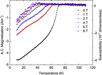
Figure 11. Ac magnetisation and magnetic susceptibility as a function of temperature of Y1MHA(3) sample. The data were taken with an excitation field of 0.4 mT and at a frequency of 777 Hz.
Download figure:
Standard image High-resolution image
Figure 12. Ac magnetisation and magnetic susceptibility as a function of temperature of Y2MHA(2) sample. No superconductivity is observed. Inset: ac magnetic susceptibility as a function of temperature of Y2MHA(3) sample which was annealed three times. The data were taken with an excitation field of 0.4 mT and at a frequency of 777 Hz.
Download figure:
Standard image High-resolution imageFor an anisotropic superconductor, we can find an approximate value for the angular dependence of the G–L penetration depth  from the angular dependence of the G–L coherence length
  derived from upper critical field, and the angular dependence of the G–L constant
  where
where  [57] so that

and

By integrating equation (5) or (6) over all solid angles, we obtain an angular average where for example  the angular average of the inverse of the G–L penetration depth squared, for a collection of random oriented grains, is

Numerical integration of equation (7) with values of  = 916 nm and
  = 138 nm [19] and using an average grain size of 100 nm, gives
  = 1.8 × 10⁻². This value is similar to that given in figure 11 for Y1MHA(3) and figure 12 inset for Y2MHA(3), consistent with a reversible ac signal entirely from within the nanocrystalline grains. We note that this calculation does not account for the induced moment and the applied field not being parallel or demagnetisation factors [58]. Figure 13 shows the irreversibility field
  as a function of temperature for our samples, taken from the onset of the ac susceptibility data. The data were fitted using the equation [31].

where  The grains in the Y1HA and Y2HA samples have the highest superconducting critical properties of our samples. Of the microcrystalline materials, Y1H and Y2H have among the lowest
  and
and  lower than Y1MHA(3) and Y1MPA, which demonstrates the severity of the oxygen loss that the samples suffered during the HIP process. The onset
  and
and  values derived using equation (8) are listed in table 2.

Figure 13. Irreversibility field as a function of temperature of all the micro and nanocrystalline fabricated samples.  is defined as the onset in susceptibility measurements and the data fitted using an equation of the form of equation (8).
Download figure:
Standard image High-resolution image3.3. DC magnetic hysteresis
Dc magnetisation hysteresis data were also taken with the PPMS. At each temperature, the field was swept from 0 T down to −1.5 T (or –2 T in some cases), then swept up to 8.5 T and back to –1.5 T. This approach meant we could extract values of  as the magnetisation changed from the upper branch to the lower branch, as well as magnetisation
  values calculated using Bean's model [59], as shown in table 2. For pellets of radius
  and volume

where  is the difference in magnetic moment between the increasing and decreasing field branches. For rectangular bars with length
  and width

Typical hysteresis and  data for microcrystalline materials are shown in figures 14 and 15. In this paper, we assume that the currents flowing are either entirely intergranular or intragranular, or both. We set aside the possibility of clusters of well-connected grains. Given that the measured transport
  is only of the order of 105 Am–2 in microcrystalline materials, intergranular
  contributes typically less than 1% of the total dc magnetisation signal in-field and can be ignored. Hence we conclude that the dc magnetisation signal comes predominantly from hysteretic screening currents flowing within grains. The typical response for nanocrystalline materials is shown in figure 16. The data show a paramagnetic background with superconducting hysteresis which has been observed in ac susceptibility data in other granular materials in the literature [60, 61]. The lower panel of figure 16 shows the data after the paramagnetic background has been subtracted, showing a typical Type-II superconductor hysteresis curve. Straumal et al [62, 63] have shown that in ZnO, a high density of grain boundaries leads to ferromagnetism even without doping, but also that the solubility of magnetic contaminants such as Co can significantly increase with the density of grain boundaries. To investigate the effect of contamination, the WC/Co vial and balls were milled without any powder (except for that caked onto the surfaces) which yielded mainly WC/Co powder with small amounts of YBCO. The contaminants were pressed into a pellet and measured using the same method as the superconducting samples. These data are shown in the inset of figure 16. The magnetisation of contaminants are temperature-independent around 0 T, which is different to the background from the sample, consistent with the expectation that the extent of WC/Co contamination and its ferromagnetic contribution to the magnetisation are low. Hence, as with the microcrystalline samples, the dc magnetisation signal from the nanocrystalline samples is almost entirely due to screening currents flowing within the grains. Figure 17 shows a compilation of the intragranular magnetisation
  for both the microcrystalline and nanocrystalline samples (we note that the uncertainty in the grain size is typically about a factor of two) and also contains transport
  values for commercial YBCO tape [13]. Given that in our polycrystalline samples the current flows both along the ab-planes and along the c-direction, whereas
  values in commercial tapes only flows along the ab-plane for the two configurations given, figure 17 shows that the intragranular
  values in our polycrystalline samples are high. The best microcrystalline samples have intragranular
  comparable to that of tapes, and strikingly the field dependence for all the samples that have been annealed is very similar to the commercial tapes. The samples that were HIP'ed-only (Y1H and Y2H) show a more drastic decrease in
  with magnetic field compared to other microcrystalline samples, and at 8 T, have
  comparable to that of the nanocrystalline group. We attribute the poorer in-field properties of some of our samples to the decrease in oxygen content during HIP'ing, consistent with the decrease in
  and
and  seen in the ac susceptibility data. After annealing (Y1HA and Y2HA),
 and
and  have all recovered. Compared to commercial YBCO tape, transport
  of microcrystalline materials is 106 lower, and for nanocrystalline material Y2MHA(2) (not included on this graph) this difference increases to 109.

Figure 14. Magnetisation as a function of field for Y1P at temperatures from 4 to 90 K and between −2 and 8 T. The data at −2 T have a gradient of 
Download figure:
Standard image High-resolution image
Figure 15. Critical current density as a function of field for Y1P, at temperatures from 4 to 90 K and between −2 and 8 T. Grain dimensions were used to calculate magnetisation 
Download figure:
Standard image High-resolution image
Figure 16. Upper panel: hysteretic magnetisation of Y1MHA(1) sample. Inset: magnetisation of the milling materials (that are potential contaminants in the samples). Lower panel: the same hysteretic magnetisation data as the upper panel, after subtracting the paramagnetic background, that show typical Type-II hysteresis and temperature dependence.
Download figure:
Standard image High-resolution image
Figure 17. Magnetisation  as a function of field for fabricated samples at 4.2 K (unless otherwise labelled). Grain dimensions were used to calculate magnetisation
  Transport
  of Y1HA sample (shown in the lower panel) and YBCO commercial tape data are also included for comparison [13]. The best microcrystalline samples have intragranular
  comparable to that of tapes.
Download figure:
Standard image High-resolution imageIn addition to finding a clear intragranular signal associated with superconductivity for the nanocrystalline materials, not found using standard ac susceptibility measurements, we can use field reversal in the dc magnetisation measurements  With these data we can address the type of pinning. Using Bean's relation for a cylinder,
  where
where  is the magnitude of the field required to reverse the magnetisation, equation (9) gives [64]
where the negative sign comes from Lenz's law. Figure 18 shows minor hysteresis loops taken at 10 K for Y1P. The inset of figure 18 shows that  is only weakly field dependent. At very low fields,
  increases, associated with the increased role of reversible screening currents flowing at the surface of the sample. The
  values in table 2 were obtained from the field reversal data at –1.5 or –2 T, calculated from the linear region during the initial field reversal. In most microcrystalline materials, typical values of
  are approximately –0.17, consistent with bulk pinning in Bean's model. For nanocrystalline materials, the values of
  derived from data similar to that in figure 16 are typically 3 orders of magnitude smaller. These small values, compiled in table 2, have been found in the work of Shimizu and Ito [65] and cannot be explained by bulk pinning using Bean's model. We attribute the low values to the surface pinning in the grains, consistent with dc magnetisation signals that are predominantly intragranular. Hence, the magnetisation
  we have calculated using grain size dimensions, provides a lower bound for the grain's surface pinning
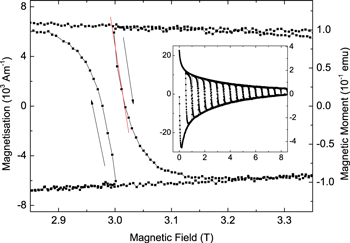
Figure 18. Magnetisation hysteresis as a function of magnetic field in order to study field reversal for the Y1P sample at 4.2 K. Starting from zero field, the field was repeatedly ramped +1 T then −0.5 T, up to 8.5 T. Inset: field reversal data set showing the full range. The arrows show the direction of the hysteresis and have a gradient for 
Download figure:
Standard image High-resolution image4. Theoretical considerations
By using a combination of transport and ac magnetic susceptibility data, we can separately determine the magnitude of the intergranular current density and the intragranular current density. In this section we consider grain and grain boundary properties. We use our resistivity data and the theoretical considerations to explain why the transport current density is so low in our YBCO samples.
4.1. The limiting size for superconductivity
While fabricating nanocrystalline materials, it is reasonable to ask first, how small grains can be before they can no longer be considered bulk material. Deutscher et al [66] have provided three methods for calculating the minimum size required to sustain superconductivity in LTSs. The first is the condition that superconductivity is quenched when the fluctuations in the order parameter  are of the same order as the order parameter
  which leads to

where  is the condensation energy and
  is the minimum volume of a grain that still sustains superconductivity. The second is when there is only one Cooper pair per grain so that

where  is the density of states at
  and
and  is the superconducting energy gap. The third is when the separation of quasi-particle energy levels
  is of the order of
  which leads to the equation

where  is the minimum radius and
  is the Fermi wavelength. Deutscher made assumptions that are only strictly justified for LTSs. However, if we naively apply these methods to YBCO, then we obtain
  = 0.3–1 nm (using literature values of
  = 0.063
  per unit cell [67],
  = 2.10 × 1028 m–3 eV–1 [68],
  = 30 meV [59],
  = 0.3 nm [69] and
  = 1.5 nm [70]). These calculations suggest even the (100 nm) grains in our nanocrystalline YBCO are sufficiently large to be well within the bulk material regime.
4.2. The resistivity of the grain boundaries
Without understanding why high angle grain boundaries do not support high  we cannot know why
  is low in polycrystalline materials. The standard explanation for the Dimos results that showed
  decreases with increased misorientation angle in [001] tilt boundaries is that grain boundaries act as 'weak-links'. However, this does not clarify whether the low
  values found by Dimos were due to poor coupling across the grain boundaries or weak flux pinning in the grain boundaries. TDGL calculations suggest that the surface properties at the ends of any junction strongly affect the current the junction can carry as well as the interior of the junction, which undermines comparisons between single junctions and bulk properties. Other possible explanations for low
  values could include the nature of the fundamental mechanism for superconductivity itself or perhaps the underlying symmetry of the
  -wave order parameter. The low carrier density or specific electronic structure that leads to HTS or the phononic structure may also have been responsible. Despite the range of possibilities, a review of the literature shows that in S-N-S junctions, the effective resistivity of the normal layer in the junction can easily vary from a factor of 102 times higher than the bulk resistivity of normal material in the junction, as found for Pb/Cd/Pb [71], and up to a factor of 104 times higher, as is the case for Nb/Al/Nb [72] [73], Pb/Cu/Pb [74] [75], and YBCO/Au/YBCO [76]. Recent work in our group on YBCO tapes has shown that large interfacial resistances of 2.5 × 10⁻⁸ Ω cm2 can even occur between a silver interface and a YBCO layer [77]. Given the potential for highly resistive interfaces and highly resistive grain boundaries in YBCO, in this paper we try to quantify how much the high resistivity of the grain boundaries lowers the critical current density of polycrystalline YBCO. We consider the most simple case, where the grain boundaries are modelled as a highly resistive N-component (i.e. where the normal layer has
  = 0) of an S-N-S junction.
We first calculate the expected resistivity of a randomly aligned polycrystalline YBCO sample with completely transparent grain boundaries (i.e. normal grain boundaries with zero resistivity). The angular resistivity  of a YBCO single crystal when the transport current is at angle
  with the c-axis in spherical coordinates is given by [78]:

where  is the resistivity along the c-axis and
  is the resistivity along the ab-plane. Integrating
  through all solid angles, gives the angular averaged resistivity
  where:

In equating  to the resistivity of a randomly aligned polycrystalline material, one is assuming that there is no redistribution or preferential percolation of the current along low resistivity paths. We can assess whether this approach is valid by considering polycrystalline graphite. Graphite is a good choice because it has very low resistivity grain boundaries. Single crystal resistivity values for graphite are:
  and
and  [79]. Polycrystalline graphite has a resistivity of
  [80] which is consistent with the value of
  from equation (16). A similar calculation for YBCO using the resistivity of single crystals, where
  and
and  at 100 K [81], gives
 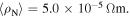 Figure 6 shows the resistivity of sample Y1HA and compares it to values for single crystals and
  Sample Y1HA has a resistivity about 50% higher than
  . Given the very high values of critical parameters for the grains of this material (
 and magnetisation
  ), we attribute the enhanced resistivity (2.4 × 10⁻⁵ Ωm) to the resistivity of grain boundaries. Using a grain size of approximately 5 μm and a grain boundary thickness of approximately 1 nm [82] leads to a large grain boundary resistivity of
  Using a similar approach to the resistivity data for the nanocrystalline materials in table 2, a grain size of 100 nm gives a very large grain boundary resistivity of
  In terms of contact (areal) resistivity, the micro and nanocrystalline grain boundary resistivities are
  and
and  respectively. These values can be compared to the contact resistivities for some [001] tilt grain boundaries in thin-film oxide bicrystals (including YBCO) [83], which are generally lower and in the range of
  –
–  We note that one can expect the resistivity of grain boundaries with misorientation angles that can include all possible angles to be higher than the [001] tilt, strain-free bicrystal grain boundaries. The resistivity data in figure 6 for Y1HA also provide supporting evidence for the additional resistance of the grain boundaries being similar to that of the grains: after the initial onset of the superconducting transition of the grains at 92 K, there is an inflection at ∼83 K, which we attribute to the grain boundaries starting to carry significant current. The lower temperature part of the transition is much more strongly depressed by the magnetic field than the onset transition which is similar to that observed elsewhere [36] and consistent with the in-field properties of grain boundaries [3].
4.3. Depairing current density of the grain boundaries
In this section we calculate the reduction in the local depairing current density  in the boundary caused by its high resistivity. Recently we have found analytic solutions to the G–L equations in zero field for the
  in a 1D S-N-S junction in the clean and dirty limit [8] where:
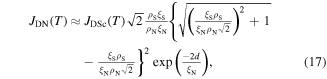
where  is the depairing current density in the superconducting grain,
  is the ratio of the resistivity in the grain to the grain boundary,
  is the ratio of the G–L coherence length in the superconductor to the decay length of the order parameter in the normal grain boundary, and
  is the thickness of the grain boundary. Because equation (17) provides zero-field values, we use it to provide upper bound values for
  in the grain boundaries of polycrystalline YBCO (
 values in table 1 were used in these calculations). To simplify the analysis for the anisotropic materials, we have only considered angular averaged properties to calculate an angular average for
  (i.e.
(i.e.  ) in table 3, where we have used

where  and
and  are the angular average G–L penetration depth and G–L coherence length and can be found in table 1. The superconducting parameters in equation (17) are well established. Microscopic theory gives the clean coherence length as

and the dirty coherence length

where  is the critical temperature of the superconducting layer. We can use the relation for the diffusivity given by:

where the equivalent forms in equation (21) have been derived using standard relations [84] for resistivity and the Sommerfeld constant  and also for the angular averaged Fermi velocity
  and mean free path
  in terms of number of valence electrons per unit volume
  Accurate values of these microscopic parameters are critical to the calculation of
  To test the validity of these values listed in table 3, we used Pippard's approach to find a coherence length
  from the clean and dirty values [8] using

We suggest that the microscopic parameters are reasonable values since a comparison between  and
and  (see table 3), shows they are similar. We have used the Ginzburg–Landau relation (that is strictly only valid close to
  ) to define
  where
where

Within the context of the G–L theory, the temperature dependence of  is given by

We have followed Pippard's approach and related  to the microscopic clean and dirty limits [8] using
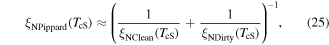
where


in which  is the normal layer equivalent of
  as given by equation (21) and
  is the critical temperature of the normal layer. The largest uncertainties in calculating
  are associated with the values of the microscopic properties of the grain boundaries. We have simplified the analysis by assuming that grain boundary structures are not superconducting (i.e.
  ) and that we can use resistivity to characterise the difference between the microscopic properties of the grains and the grain boundaries. Grain boundaries are complex structures and one can expect that when their resistivity changes, their carrier concentration, effective width and scattering time all change. Our assumptions lead to
  and
and
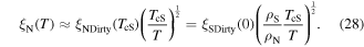
As a starting point for calculating  in table 3 we have assumed that the grain boundary thicknesses in all the materials (i.e.
  in equation (17)) is 1 nm. Equations (17) and (28) show that as the resistivity of the grain boundaries increases,
  decreases and
  is severely depressed. In the microcrystalline YBCO materials of this work, the resistivity is more than three orders of magnitude higher than the grains, which by itself provides a straightforward explanation for the very low transport current densities we have experimentally measured. The calculations of
  are particularly sensitive to the values of
  and
and  Once
Once  is smaller than
  the exponential term in equation (17) dominates. In this regime, small increases in
  produce very large reductions in
  The resistivity of our nanocrystalline materials is even higher than the microcrystalline values and
  even lower. We note that these very high values of resistivity are beyond the Ioffe–Regel criterion (i.e.
  [85]). However, we conclude that even the straightforward analysis provided here demonstrates that the values of grain boundary resistivity we have measured in microcrystalline and nanocrystalline materials are sufficient to explain the low values of our transport
  data.
data.
Table 3.
Resistivity of the normal layer  at
at  Sommerfeld constant
  Fermi velocity
  the superconducting layer coherence length in the clean and dirty limits (
 and
and  ), comparison of the Pippard coherence length
  with the
  coherence length calculated from
  where
where 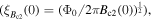 the normal layer diffusivity
  calculated using
  values, decay length of the normal layer in a Josephson junction
  and the ratio of the local depairing current density of the grain boundary to the depairing current density of the superconductor:
  given by equation (17). For angular averaged (A.A.), microcrystalline and nanocrystalline YBCO, we have taken the resistivity values from measurements in this work and assumed that the grain boundaries are 1 nm thick. For all other materials, we have again assumed that the grain boundaries are 1 nm thick normal grain boundaries, but that the resistivity is equal to the resistivity of the grains. For all materials, we have assumed that the Sommerfeld constant and the Fermi velocity are an angular average in the calculation of
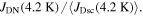
| Material |
 (Ω m) (Ω m) |
 (J m−3 K−2) (J m−3 K−2) |
 (105 m s−1) (105 m s−1) |
 (nm) (nm) |
 (nm) (nm) |
  (nm) (nm) |
 (m2 s−1) (m2 s−1) |
 (nm) (nm) |

|
|---|---|---|---|---|---|---|---|---|---|
| NbTi | 4.0 × 10⁻⁷ | 1.1 × 10³ | 2.0 | 31 | 4.3 | 3.8 | 5.7 × 10⁻⁵ | 6.4 | 0.28 |
| [127] | [127] | [59, 127] | 4.6 | ||||||
| Nb3Sn | 8.8 × 10⁻⁸ | 1.2 × 10³ | 0.60 | 4.6 | 6.3 | 2.7 | 2.4 × 10⁻⁴ | 13 | 0.21 |
| [16] | [33] | [128] | 3.3 | ||||||
| PbMo6S8 | 7.0 × 10⁻⁷ | 3.8 × 10² | 0.40 | 4.0 | 4.5 | 2.1 | 9.2 × 10⁻⁵ | 8.1 | 0.21 |
| [34] | [34] | [128] | 2.4 | ||||||
| MgB2 | 1.0 × 10⁻⁶ | 1.5 × 10² | 6.1 | 22 | 3.5 | 3.0 | 1.6 × 10⁻⁴ | 10 | 0.28 |
| (A.A.) | [129] | [130] | [131] | 4.3 | |||||
| YBa2Cu3O7−x | 5.0 × 10⁻⁷ | 2.0 × 10² | 5.0 | 7.5 | 2.8 | 2.1 | 2.4 × 10⁻⁴ | 13 | 0.16 |
| (ab-plane) | [132] | [56] | 1.5 | ||||||
| YBa2Cu3O7−x | 5.0 × 10⁻⁵ | 2.0 × 10² | 5.0 | 7.5 | 0.28 | 0.27 | 2.4 × 10⁻⁶ | 1.3 | 0.077 |
| (A.A., 5 μm) | [132] | [56] | 1.5 | ||||||
| YBa2Cu3O7−x | 1.2 × 10⁻¹ | 2.0 × 10² | 5.0 | 7.5 | 0.28 | 0.27 | 1.0 × 10⁻⁹ | 0.027 | 10−35 |
| (Micro, 5 μm) | [132] | [56] | 1.5 | ||||||
| YBa2Cu3O7−x | 8.2 | 2.0 × 10² | 5.0 | 7.5 | 0.28 | 0.27 | 1.5 × 10⁻¹¹ | 0.0033 | 10−270 |
| (Nano, 100 nm) | [132] | [56] | 1.5 |
5. Discussion
5.1. Micro- and nanocrystalline YBCO
We have found, using a combination of transport measurements and ac magnetic susceptibility measurements, that our nano- and microcrystalline YBCO can be considered to be high quality grains surrounded by non-superconducting highly resistive grain boundaries that limit transport  The current densities within the grains are high and those across the grain boundaries low. We have adopted a pragmatic approach to the analysis of the grain boundaries in our samples and used angular averages for this strongly anisotropic material and ignored percolation. We have also adopted a simple two-component description of our materials as grains and grain boundaries and used an S-N-S description that assumes that the pinning is sufficiently strong along the grain boundaries that
  is determined by the local depairing current density in the grain boundaries themselves. One can expect in superconducting materials there are a range of different length scales for the variations in composition, strain and physical structure as well as electronic and phononic structure. Although it is reasonable for us to have assumed that grain boundary structures are not superconducting themselves in bulk form, finding the other characteristic microscopic properties of the grain boundaries
  will be a formidable challenge. Characterising bulk materials in thin film form proved difficult enough for the scientific community with the luxury of free-standing samples, or samples on insulators and data for parent bulk samples. Grain boundaries can be considered as internal surfaces. They bring the challenges of characterising a structure that is inhomogenous, is sandwiched between two grains, and is not available in bulk form [86]. Given the large effort it has taken to understand bulk materials, one can expect an even larger effort will be required for the local normal and superconducting properties of grain boundaries.
From a technological perspective, we would like to increase  in polycrystalline YBCO if at all possible. The [001] tilt boundaries in the literature have contact resistivities which vary from
  in the low angle bicrystal data [3], up to
  for 40° boundaries [87]. The average contact resistivities in our microcrystalline samples were
  and in the nanocrystalline samples
  Higher average contact resistivity values are expected in the polycrystalline samples than bicrystals because the misorientation angles are not limited to [001] tilt grain boundaries. We have modelled grain boundaries, as simple non-superconducting resistive layers. This ignores complexities such as the possibility that very low angle grain boundaries may have non-zero critical temperature and high angle grain boundaries may be ferromagnetic [62, 63], which in the G–L framework can be described using negative local critical temperatures. However, table 3 shows that even if we just apply our simple model, and reduce the grain boundary resistivity to be the same as the grains, the value of
  along the ab-plane is still 0.16, which is similar to that in the best YBCO tapes. For bulk YBCO with equal grain and grain boundary resistivity,
  is further reduced to 0.077. We may hope that faceted grain boundaries [88] may help but given the high grain boundary resistivities found at high angles in bicrystal data, it seems unlikely that grain boundary engineering will enable high
  in polycrystalline YBCO. Grain boundary engineering such as Ca doping has successfully reduced grain boundary contact resistivity by over an order of magnitude and increased
  by a factor of 6–7, however these results were on bicrystals preferentially doped at grain boundaries [5], thin film bicrystals [89] or multilayer films [90]. We consider it unlikely that one can reduce the grain boundary resistivity in polycrystalline materials to be less than that of the grains themselves and therefore that grain boundary engineering is unlikely to be successful in increasing
  to technologically useful values, in randomly aligned polycrystalline YBCO.
5.2. Improving  in LTS and HTS high-field superconductors

The data in the second panel of figure 1 shows that in high fields, all technological superconductors have a large headroom for improvement. In applied fields of half  NbTi is only a few percent of its theoretical limit, and Nb3Sn(IT) produced using the internal tin route is only about 0.3% of its theoretical limit. Materials with the highest
  values include commercial YBCO tape [28], thin film Ba(FeCo)2As2 [91] and Nb [12] that have been fabricated with no large-angle grain boundaries. Hence one can expect high
  throughout the entire material, and strong pinning to be effective. It is unclear whether adding even more pinning will lead to further improvements, or whether the low angle grain boundaries or channels formed by contiguous strained and degraded material between pinning sites provide channels for flux flow and hence limit
  in these three materials. In addition to the thin film Ba-122 in figure 1, Ba-122 thin films with artificially engineered superlattices with strong pinning along the ab-plane and c-axis and improved
  over a wide angular range [92] have been developed. Although untextured polycrystalline bulks and wires have achieved
  of 109 Am–2 at 0 T and 4.2 K, which is more than 10 times higher than other round untextured ferropnictide wires, it is still 10 times lower than the thin film materials [93]. The materials with markedly low
  values include MgB2 [94], FeSe0.5Te0.5 [95] and the A15 polycrystalline materials [96, 97]. Excellent polycrystalline, untextured MgB2 can be produced cheaply through solid state reactions [98–101], as can FeSe0.5Te0.5 through sintering [102] or powder-in-tube process [103]. However, such FeSe0.5Te0.5 materials achieve
  values of 107 Am–2 at 0 T and 4.2 K, which are two orders of magnitude lower than the tape sample in figure 1. After Nb3Sn was discovered in 1954 [104], materials for magnets were fabricated with
  values of 1.5 × 10⁹ Am–2 at 8.8 T in 1961 [105]. By 1990,
  values of 2.2 × 10⁹ Am–2 at 11 T were achieved [106] and now state-of-the-art values are approximately 8 × 10⁹ Am–2 at 11 T. Improvements in
  are hard-earned and have enabled technological applications above 10 T including high-field MRI, particle accelerator magnets and fusion energy. However, an improvement in
  by an order of magnitude over 50 years does not seem very large in the context of a headroom of nearly 3 orders of magnitude between
  and the theoretical upper limit
  If flux flow along channels rather than pinning in the grains are the problem, equation (17) suggests high grain boundary resistivity and/or wide grain boundaries are responsible. The resistivity of Nb3Sn and the other A15 intermetallics has been studied extensively. Very large changes in resistivity have been found in Nb3Sn and V3Si with relatively small changes in composition [107]. For binary Nb3Sn,
 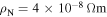 for 25 at% Sn and
 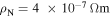 for 24.5 at% Sn. In a series of nanocrystalline HIP'ed Nb3Sn fabricated in our group, materials with 120 nm grain size and
  = 17.4 K and
  = 30 T,
 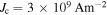 at 0 T and 5 K,
 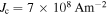 at 6 T and 5 K, were found to have resistivity values of
 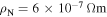 [108]. When the grain size was reduced to 20 nm,
  reduced to 10 K and
  increased to
  When the grain size was below 10 nm,
  was below 2 K and
  increased to
  [109]. These nanocrystalline results show that very high resistivity values can occur in Nb3Sn and that a non-superconducting width for the grain boundaries of 3 nm in Nb3Sn polycrystalline materials is not unreasonable. The quality of our nanocrystalline Nb3Sn materials may simply have been poor, but the sustained low
  values in state-of-the-art materials may point to a more fundamental grain boundary problem. There are other factors may also help explain why the effective width of non-superconducting grain boundaries are large in A15 compounds. Band structure calculations point to the density of states at the Fermi level being determined by the one-dimensional chains of Nb atoms [107, 110]. Variable strain measurements show that a strain as low as 1% significantly depresses
  [97, 111, 112]. Calculations using equation (17) show that for Nb3Sn, low values of
 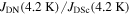 of just 0.2% can occur, when the grain boundary width is 3 nm and
  It follows that improvement in the
  of Nb3Sn can be achieved if the grain boundaries are improved or removed. However, the properties of the grains and the grain boundaries cannot be considered completely decoupled. If we improve the connectivity by lowering the resistivity of the grain boundaries, although we increase the local depairing current in the grain boundaries, we can expect to decrease the surface pinning that restrains the fluxons within the superconducting grains. Hence, we may need to add strong pinning sites into the grains themselves. Whether the improvements would be commercially viable is beyond the scope of this paper.
6. Conclusion
Micro- and nanocrystalline YBCO samples were fabricated in order to study the nature of grain boundaries. Detailed magnetic data enabled us to measure and distinguish hysteretic screening currents, limited to within the grains, from transport currents that cross grain boundaries and conclude that the magnetisation  is at least 105–106 times larger than transport
  for both our micro- and nanocrystalline materials. Using resistivity data and considering the polycrystalline material as S-N-S junctions, we have shown that high resistivity in the grain boundaries is enough by itself to reduce the local depairing current density of the grain boundaries and hence limit the transport
  For microcrystalline materials, transport
  on the order of 105 Am–2 was measured. In our nanocrystalline samples, we found there were no intergranular currents through our samples except for just one, in which
  was reduced by at least 109 compared to commercial tapes. This work has provided a quantitative description of grain boundaries that we hope can help provide a framework to extend our characterisation of grain boundaries from those in model systems and bicrystals, to those in technologically-important high-field superconducting materials that are used in commercial applications. It provides calculations that identify when grain boundaries are so resistive they limit
  in polycrystalline materials. Grain boundaries in polycrystalline technological materials are complex and inhomogeneous. We expect a more complete treatment to consider percolative effects and to provide more sophisticated measurements of local grain boundary properties.
Acknowledgments
The authors would like to thank the members of the Durham Superconductivity Group, the Durham mechanical workshop and in particular Steve Lishman, as well as Dr Y H Shi and Professor D Cardwell from Cambridge University Bulk Superconductivity Group. The data are available at: http://doi.org/10.15128/gh93gz497 and associated materials are on the Durham Research Online website: http://dro.dur.ac.uk/. This work is funded by EPSRC grant EP/K502832/1.
: Appendix
The temperature dependence of the depairing current density for a superconductor  as listed in table 1 is calculated as shown below. Our approach was broadly either to find expressions for the G–L penetration depth
  the G–L coherence length
  and
and  directly from the literature or to find the upper critical field
  and lower critical field
  at any temperature from the literature and use well known temperature dependencies for these critical fields to calculate
  and
and  In table 1, we have shown values of the critical fields and length scales at 0 K.
Appendix. A.1. Calculation of in zero field

First we consider the G–L expression for the depairing current density of an anisotropic superconducting material such as YBCO or an isotropic superconductor. When the current is in the  plane,
  is given by:

where  is the flux quantum,
  is the G–L penetration depth and
  is the G–L coherence length. Since there is no general theoretical expressions for
  we use an empirical equation of the form:

Note in equation (30) that when the applied magnetic field points in the c-axis direction, the relevant length scale is the G–L coherence length in the ab-plane. We can differentiate equation (30) with respect to  to obtain:

We use the G–L equation for  (correct only for
  ) [113]:

and the G–L expression for the G–L coherence length  which is generally taken to be true for all temperatures, of the form:

We can differentiate equation (32) with respect to  to obtain:

From equations (31) and (34) we have:

Substituting this equation into equation (33), we have:

Substituting equation (30) into (36) leads to:

The temperature dependence of  in the ab-plane can be calculated in a similar way using:

where  has been taken to have a value of 2 for all superconductors. This can be differentiated to give:

We also use the G–L relation for the G–L penetration depth, valid at all temperatures:

and the G–L relation for  [113]:
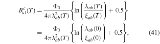
which can be differentiated to give:
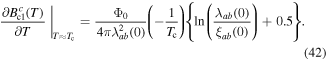
Combining equations (39) and (42) leads to:

Combining equations (38), (40) and (43) gives 
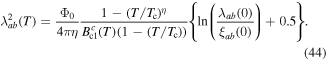
Equations (37) and (44) can be substituted into equation (29) to calculate 
A.2. Calculation of in zero field

For anisotropic materials, we can also calculate the depairing current density when the current is flowing in the c-axis direction ( ), given by:

Using the general result for anisotropic superconductors [57]:

we have:

The G–L relation for  is [113]:

and the scaling with temperature is given by:

Similar to the methods described above for current flowing in the ab-plane, by combining the derivatives of equations (48) and (49) we find:
where  can be obtained from equation (35), and
  can be found using:

Finally,  can be found given
 and
and  using equation (46). Hence we can calculate the values necessary to produce (45) and figure 1 [13–25].