

Abstract
This study presents the characterization of the nickel–vanadium (NiV) Schottky diode on n-type silicon (Si) in the temperature range 75 K–300 K. The experimental current–voltage (I–V) measurements are first analyzed by using the thermionic emission (TE) theory. For this purpose, the vertical optimization method is used to find the values of the TE parameters, i.e. the values of the ideality factor, barrier height, and series resistance. It is found that these parameters exhibit strong temperature dependence, i.e. an increase of the ideality factor and a decrease of the barrier height  and the series resistance
  when the temperature decreases, which is due to inhomogeneities at the Schottky interface. Therefore, we employ Werner's model under the assumption of a Gaussian distribution to analyze the temperature dependence of the TE parameters. The mean and standard deviation of the barrier height are obtained as
  and
and  , respectively. In addition, we show that the apparent barrier height and apparent ideality factor are in accordance with Werner's model. Furthermore, we use the modified Richardson plot to find the value of the Richardson constant. The obtained value of the latter is
  A cm−2 K−2 and is very close to the theoretical value of 112 A cm−2 K−2 of n-type Si. Finally, we investigate the temperature dependence of the ideality factor and show the validity of the T0-effect for the NiV/Si Schottky diode.
Export citation and abstract BibTeX RIS
1. Introduction
Semiconductors have very important properties that have been deeply studied, exploited, developed, and applied in the fields of microelectronics and communication. The advance that has been achieved in the development of semiconductors is the outcome of understanding the physics that connects various of their aspects, such as their physical properties, manufacturing, structure, and characterization. The key to semiconductor physics is the band theory that summarizes the charge transport processes within these materials. It is well-known that by putting a semiconductor in contact with a metal, a potential barrier is established at the interface. Depending on the nature of the used materials, the obtained component may be an ohmic contact or rectifier [1, 2]. From its discovery in 1874 to the present day, the metal-semiconductor contact, which is often called the Schottky diode, has been the subject of a great deal of research.
The established potential barrier at the metal–semiconductor interface has long been assumed homogeneous, i.e. constant over the entire surface [3]. Nevertheless, the homogeneous model includes various anomalies without any physical explanation [4–6]. Particularly, the decrease in the barrier potential, the increase of the ideality factor when the temperature decreases, and the obtained Richardson constant value  that is less than the theoretical value
  for silicon [7]. Early in the 1970s, these anomalies were attributed to interface inhomogeneities [8], which are related to various reasons. For instance, the barrier height inhomogeneity is due to non-uniform metal thickness, interface layer composition, grain boundaries, etc [9]. Other sources of the interfacial inhomogeneities can include the reaction between the metal and the semiconductor, manufacturing faults, processing remnants (dirt, contamination), native oxide, uneven doping profiles, and crystal defects [4, 5, 10–12]. Although several models have been proposed in the literature to describe these inhomogeneities, only two among them, namely Werner [4] and Tung [5, 13] models, have been able to explain the majority of anomalies. In Tung's model [5], the barrier at a metal–semiconductor interface consists of locally non-uniform but interacting patches of different barrier heights embedded in a background of uniform barrier height. Moreover, the interaction of the high barrier and low barrier is described with the help of the so-called 'saddle point'. On the other hand, in Werner's model [4], the high barrier is assumed to be distributed according to a Gaussian distribution, which usually leads to an apparent barrier height that is both temperature and bias dependent. Despite their conceptual differences, both Tung's and Werner's models have been successfully used in the interpretation of experimental results on various metal-semiconductor Schottky contacts. Indeed, several studies have been performed using Werner's model to investigate Schottky diodes [14–30], whereas other researchers have been alternatively following Tung's model to explain inhomogeneous Schottky barrier heights [19, 30–45].
Nickel–vanadium (NiV) materials have various applications in the semiconductor industry [46]. Although both nickel (Ni) and vanadium (V) Schottky contacts with n-type Si have been fabricated and characterized separately in [47] and [48], respectively, Gammon et al [35] have been the first to study the NiV/Si Schottky contact. Nevertheless, the study performed in [35] consists only of studying the temperature-related non-linearity at the NiV/Si interface. Moreover, Tung's model has been used in [35] and various flaws have been observed in the model. Indeed, the authors in [35] have reported a low accuracy of Tung's model at the lowest temperatures, which is due to the divergence at low temperatures of the two current paths built into Tung's model. To the best of our knowledge, there is no existing work that has reported the electrical transport characteristics of NiV/n-Si Schottky diode. This motivates us to study the current transport characteristics of NiV/Si Schottky diodes in a wide temperature range of 75 K–300 K.
In this paper, we characterize the NiV/Si Schottky diode on n-type silicon (Si) in the temperature range of 75 K–300 K. In order to obtain the values of the series resistance, barrier height, and ideality factor, we employ the thermionic emission (TE) theory and the vertical optimization method (VOM). Subsequently, we use Werner's model under the assumption of a Gaussian distribution of the barrier height to analyze the temperature dependence of the obtained values. For this purpose, we extract the values of various parameters that characterize the NiV/Si Schottky diode, such as the mean  and the standard deviation
  of the barrier height, as well as the voltage coefficients
  and
and  . Moreover, by means of the modified Richardson plot, and by using the obtained values of
  and
and  , we determine the corrected value of the Richardson constant. Finally, we investigate the temperature dependence of the ideality factor and show the validity of the T0 effect.
2. Experimental details
Full details on the fabrication procedure were published in [35]. In brief, however, NiV Schottky diodes were fabricated on n-type silicon (100) substrates. The substrate comprised of a highly n-doped (100) Si substrate (1.2 × 1019 cm−3) and a 2 μm lightly phosphorous doped epitaxial layer (1 × 1016 cm−3). The pseudo-vertical diodes were fabricated by first cleaning the surfaces with a standard RCA clean, followed by a 3  CF4-plasma etch in a Sentech Etchlab 200 Reactive Ion Etcher to create a mesa structure that exposed the highly doped substrate. A common Ti cathode contact was then sputtered onto the exposed and roughened highly doped surface using a Mantis QPrep Deposition System, before being annealed in a Heatpulse 610 rapid thermal annealing system for 30 s at 800 °C in argon ambient. NiV was then sputtered onto the mesa surface to form the anode contact. After wire bonding, the devices were characterized using a fully automated closed-cycle-cryostat test setup, which took current–voltage (I–V) measurements between 75 K and 300 K at 25 K intervals.
3. Results and discussion
3.1. Current–voltage characteristics
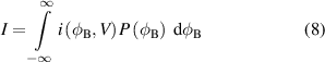
The electrical forward current–voltage ( –
– ) measurements are analyzed using the standard TE theory. According to the latter, the theoretical
  –
– relation for a metal–-semiconductor interface is given by [1, 2]
with the saturation current  defined by

where  is the inverse thermal voltage, q is the elementary electric charge, k is the Boltzmann constant, T is the temperature,
  is the series resistance of the diode, V is the applied voltage, n is the ideality factor, A is the diode area,
  is the effective Richardson constant, and
  is the barrier height.
The obtained experimental  –
– curves of the NiV/Si diode are shown in figure 1 for various values of the temperature. Our objective then is to find the values of the parameters in equation (1) that best fit the experimental I–V data, i.e. find the values of the ideality factor
  , the saturation current
  , and the series resistance
  . The barrier height can then be found by using equation (2) and the theoretical value of Richardson constant
  of n-type Si [7]. A simple approach that can be used to perform this task is the standard method, which neglects the series resistance and deduces, respectively,
  and
and  from the slope and intercept of the linear region of the
  vs.
vs.  curve. The linear fitting of the standard method for the case of the NiV/Si diode is shown in figure 1 (dashed lines). As can be seen from this figure, at each temperature, the linear fitting is only valid for a portion of the I–V curve, which is due to the existence of non-zero series resistance. For the purpose of finding the values of
  ,
,  , and
, and  that best fit the
  –
– data in all regions, we use the VOM [49, 50]. Let
  and
and  be the
  measured current and voltage at a given temperature
  , respectively, and
  be the corresponding theoretical current obtained by setting
  in equation (1). The VOM seeks to find the values of the parameters
  ,
,  , and
, and  that minimize the cost function given by
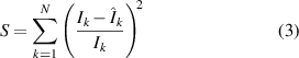
Figure 1. The experimental and fitted (I–V) plots at different temperatures. The dashed lines represent the linear fitting of the standard method and the solid lines represent the fitting by using the VOM.
Download figure:
Standard image High-resolution imagewith  being the total number of measurements. Therefore, the values of
  ,
,  , and
, and  can be obtained by solving the system of equations given by
which we have solved by using Newton–Raphson's method [50, 51]. The obtained results of  ,
,  ,
,  and
and  for various values of the temperature, are shown in figure 2. Moreover, the theoretical I–V curves obtained from equation (1) with the corresponding values of the parameters obtained by the VOM are shown in figure 1 (solid lines). It is evident from figure 1 that the experimental and theoretical results exhibit excellent agreement. Furthermore, it can be seen from the results in figure 2 that, as the temperature increases, the values of the barrier height and the series resistance increase (from
  and
and  at
at  to
to  and
and  at
at  ), whereas the value of the ideality factor decreases (from
  at
at  to
to  at
at  ).
).
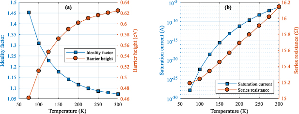
Figure 2. The obtained values of the parameters of the NiV/Si Schottky diode as functions of the temperature. (a) Ideality factor and barrier height. (b) Saturation current and series resistance.
Download figure:
Standard image High-resolution imageIn figure 3, the experimental reverse bias I–V curves are shown for the temperature range 250 K–300 K. It should be noted, however, that the reverse bias I–V curves for temperatures lower than 250 K are not shown here due to the smallness of their reverse bias current values, which are lower than the precision of our measuring equipment, and thus very noisy and unreliable. From the reverse bias curves shown in figure 3, the value of the reverse saturation current is obtained as  ,
,  , and
, and  A for the temperature values of
  K,
K,  K, and
  K, respectively. These values are very close to their corresponding values obtained from the forward bias curves as can be seen from figure 2(b). From these results and those of the saturation current shown in figure 2(b), it is evident that the saturation current decreases with decreasing temperatures, which is in accordance with the TE theory prediction. Furthermore, the reverse bias I–V curves in figure 3 and their forward counterparts in figure 1 demonstrate clearly that the NiV/Si Schottky diode has a very good forward-to-reverse (rectification) current ratio. For instance, at a voltage of
  V, the rectification ration is of order
  ,
,  , and
, and  for the temperature values of
  K,
K,  K, and
  K, respectively.
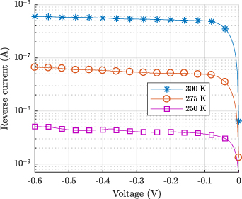
Figure 3. The reverse bias I–V curves of the NiV/Si Schottky diode.
Download figure:
Standard image High-resolution imageThe temperature dependence of the ideality factor and the barrier height that are reported above are due to the inhomogeneities of the Schottky barrier. Indeed, the linear relation between the barrier height and ideality factor is demonstrated in figure 4 and it is a signature of inhomogeneities [5, 52, 53].
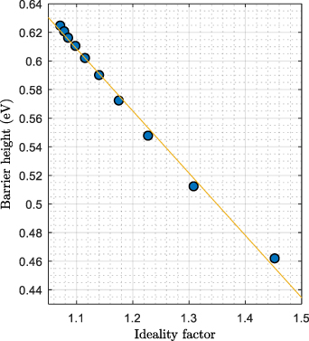
Figure 4. The relation between the barrier height and the ideality factor.
Download figure:
Standard image High-resolution image3.2. Inhomogeneous barrier analysis
As mentioned earlier in the introduction section, the inhomogeneities of the Schottky barrier can be explained by using Werner's model under the assumption of a Gaussian distribution of the barrier height. The probability density function of the barrier height is given by
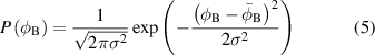
where  ,
,  , and
, and  are the barrier height, its mean, and its standard deviation, respectively. Furthermore, a linear bias of
  and quadratic bias dependence of
  are assumed in Werner's model, i.e.

and

where  and
and  are coefficients that are temperature independent. Hence, the total current across the Schottky contact can be obtained as
with  being the current at a given barrier height
  and voltage
  . By substituting
  and
and  from equations (1) and (5), respectively, equation (8) yields
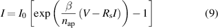
where

 and
and  are, respectively, the apparent barrier height and the apparent ideality factor, which are given in Werner's model [4, 22, 23, 54] by
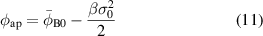
and
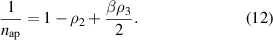
According to equation (11), the plot of  versus
  should be a straight line. The plot of
  versus
  for the NiV/Si diode is given in in figure 5. As shown in this figure, the results are in good agreement with equation (11), and thus the values
  and
and  are obtained from this plot. Figure 6 shows the (
 ) versus
  plot of the NiV/Si diode. As seen, the obtained results are in accordance with equation (12). Therefore, the values of the voltage coefficients
  and
and  can be obtained, respectively, from the intercept and the slope of the curve in figure 6 as
  and
and 
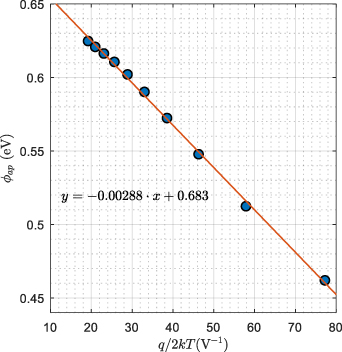
Figure 5. The apparent barrier height  versus
  .
.
Download figure:
Standard image High-resolution image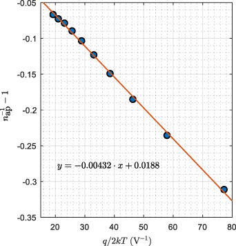
Figure 6. The ( ) versus
  curve of the NiV/Si Schottky diode according to the Gaussian distribution.
Download figure:
Standard image High-resolution image3.3. Richardson and modified Richardson plots
The conventional Richardson plot of  versus
  is usually used to determine the Richardson constant
  and the barrier height
  . Figure 7 shows the conventional Richardson plot for the NiV/Si diode from which the values of the barrier height and the Richardson constant are obtained as
  and
and  A cm−2 K−2, respectively. However, the obtained value of the Richardson constant is much smaller than the theoretical value of 112 A cm−2 K−2 of n-type Si [7]. The small value of the Richardson constant suggests that the effective area is much smaller than the diode area [18]. Moreover, it is apparent from figure 7 that the conventional Richardson plot deviates from linearity, which is due to the inhomogeneity of the barrier height [54, 55]. This anomalous behavior can be explained by taking into account the inhomogeneity of the barrier height, which can be achieved by combining equation (10) and equation (11) as
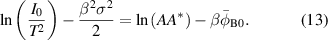
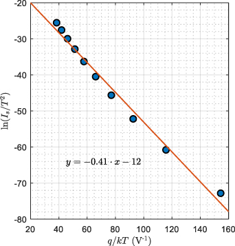
Figure 7. The conventional Richardson plot for the NiV/Si Schottky diode.
Download figure:
Standard image High-resolution image
The modified Richardson plot of  versus
  for the NiV/Si Schottky diode according to equation (13) is shown in figure 8. As seen, the plot is well-fitted by a straight line that gives
  eV and
  A cm-2 K-2 from the intercept and slope, respectively. The obtained value of
  matches perfectly the previously calculated mean barrier height that has been obtained from the plot of figure 5 (see section 3.2). Furthermore, the obtained value of the Richardson constant is very close to the theoretical value of 112 A cm-2 K-2 of n-type Si. These results clearly indicate the usefulness and validity of the modified Richardson plot.
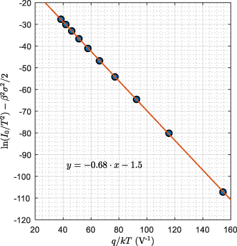
Figure 8. The modified Richardson plot for the NiV/Si Schottky diode.
Download figure:
Standard image High-resolution image3.4. T0 effect
The variation of the ideality factor with temperature in Schottky diodes is known as the T0 effect, or alternatively, as the T0 anomaly [18, 56]. According to Saxena [57], the temperature dependence of the ideality factor is usually given by
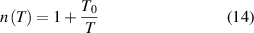
where  is a positive constant that is referred to as the excess temperature. On the other hand, according to Werner, the temperature dependence of the ideality factor can be obtained from equation (15) as
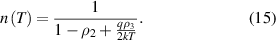
In the case of  , which is valid for most cases of Schottky diodes [23],
  in equation (15) can be approximated as [23]
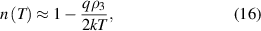
which is of the same form as equation (14). Therefore, by comparing equation (14) and equation (16), a theoretical approximation of  can be obtained as
By using the calculated value of  , we obtain from equation (17),
  . Figure 9 shows the experimental
  versus
  plot together with its linear fitting and illustrates the temperature dependence of the ideality factor for the NiV/Si Schottky diode. In the same figure, the
  versus
  plot corresponding to equation (16) with the calculated value of
  is shown as well. As can be seen from figure 9, equation (16) well approximates the temperature dependence of the ideality factor. Nevertheless, it is evident that, in contrast to equation (16), the slope of the experimental data deviates slightly from unity. Such deviation of the slope has been observed in various Schottky diodes [23] and it is mainly due to the temperature dependence of T0 [49, 56]. In addition, equation (16) is derived from an approximation that may not always be accurate [56]. Indeed, in our case, the condition of
  is weakly valid in the considered temperature range. Therefore, as has been reported in several works [18, 23, 56, 58, 59], the temperature dependence of the ideality factor, in this case, is given by
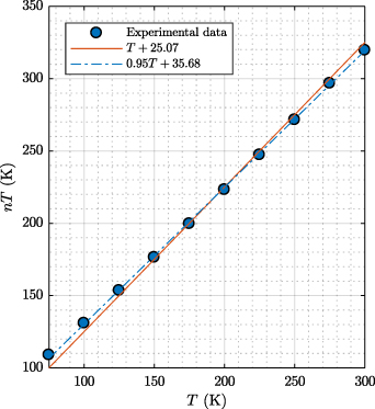
Figure 9. Plot of  versus
  for the NiV/Si Schottky diode indicating the temperature dependence of the ideality factor.
Download figure:
Standard image High-resolution image
with  and
and  can be obtained for the NiV/Si diode from the slope and intercept of the linear fitting of the experimental
  versus
  plot as
  and
and  . As demonstrated in figure 9, with the obtained values of
  and
and  , equation (18) describes the temperature dependence of the ideality factor more accurately than equation (16).
4. Conclusion
In this paper, the temperature dependence of the I–V characteristics of the NiV/Si Schottky diode has been reported in the 75 K–300 K temperature range. The I–V measurements have been analyzed by using the TE theory. For this purpose, the VOM has been used in order to find the values of the ideality factor, barrier height, and series resistance that best fit the experimental I–V measurements. It has been established that the ideality factor, barrier height, and series resistance vary, respectively, in the ranges of 1.07–1.453, 0.461–0.624 eV, and 15.188–16.145  . Moreover, it has been observed that in contrast to the ideality factor, which decreases when the temperature increases, both the barrier height and series resistance increase when the temperature increases. This temperature dependence has been attributed to the inhomogeneities of the barrier height at the Schottky interface. Therefore, in order to consider these inhomogeneities, we have used Werner's model under the assumption of a Gaussian distribution of the barrier height. The mean and standard deviation of the barrier height have been obtained as
  and
and  mV, respectively. Moreover, the experimental results of the apparent ideality factor and barrier height have been found to fit well with Werner's model. Furthermore, by means of the modified Richardson plot of
  versus
  , the value of the Richardson constant has been obtained as
  A cm−2 K−2, which is very close to the theoretical value of 112 A cm−2 K−2 of n-type Si. Finally, the T0-effect has been investigated and it has been shown that the experimental results of the ideality factor fit well with the well-known equation
  with
with  and
and  .
.