

Abstract
In this paper, process variability such as random dopant fluctuation (RDF), work function variation (WFV), and oxide thickness variation (OTV) in 14 nm node junctionless (JL) FinFETs is investigated using the impedance field method (IFM). Effects of doping concentration, gate metal grain-related parameters, and device parameter scaling on RDF, WFV, and OTV induced variability are studied using the standard deviations of threshold voltage (σVth) and subthreshold slope (σSsub). As a result, we find that a relatively low doping concentration helps alleviate process variability. As average grain size increases, different mechanisms of σVth and σSsub degradation are analyzed for WFV and OTV induced variability. Compared to WFV and OTV, RDF is revealed as the most significant source of variability as devices scale down. It is observed that fin width (Wfin) and oxide thickness (tox) scaling leads to the reduction of RDF induced variability, whereas channel length (L) and fin height (Hfin) scaling results in aggravation of RDF, WFV, and OTV induced variability.
Export citation and abstract BibTeX RIS
1. Introduction
Since FinFET was proposed a few years ago as a breakthrough to overcome short-channel effects (SCEs), it has become a mainstream design in the IC fabrication industry [1, 2]. FinFET has triple gates which can control its channel and suppress SCEs better than a planar single-gate MOSFET [1, 3]. As the channel length is reduced with the improvement of fabrication processes, the fabrication of the source/drain junctions causes problems [4, 5]. During the thermal process of forming the source and drain, the dopants in the source and drain diffuse into the channel region and degrade the device's electrical characteristics.
On the other hand, Junctionless (JL) FinFETs with a uniform doping concentration in the source, drain, and channel were proposed by Lee CW et al in 2009 [6]. Due to the absence of junctions, JL FinFETs can be simply fabricated. JL FinFETs were successfully fabricated on an insulator [6, 7], and according to a study by Colinge J-P et al the subthreshold slope (Ssub) was only 64 mV dec−1 which is much lower than that of junction-based inversion mode (IM) FinFETs [7]. Hence, JL FinFETs are regarded as a substitute for IM FinFETs.
As devices shrink, process variability has become a significant issue not only for IM FinFETs but also for JL FinFETs [8–14]. The fluctuation of the number and position of dopants is called random dopant fluctuation (RDF) [12]. Although probing methods of 3D carrier profiling are developed for nano devices, it is still difficult to measure [15, 16]. Also, the random nature of grain formulation during gate electrode formation brings about work function variation (WFV) and oxide thickness variation (OTV) [13, 14]. These uncertainties can lead to significant variability of electrical parameters such as Vth and Ssub. If process variability is inevitable in the fabrication process, it is necessary for device engineers to analyze and reduce the sources of variability. To show the significance of variability analysis, previous studies addressed the RDF and WFV of JL FinFETs using atomistic simulations [8–11]. However, they assumed a fixed average gate metal grain size and failed to show the relation of the grain size to the variability of subthreshold characteristics [9, 10]. Also, OTV in JL FinFETs was not analyzed but should be compared with RDF and WFV. Hence, statistical analysis of RDF, WFV, and OTV as a function of the grain size of the gate metal in JL FinFETs is required.
In this paper, the comparative process variability including RDF, WFV, and OTV in JL FinFETs is statistically analyzed. The effects of doping concentration, grain-related parameters, and device parameter scaling on the variability sources are investigated. The process variability is evaluated using the standard deviation of the threshold voltage (σVth) and subthreshold slope (σSsub).
2. Device structure and simulation calibration
2.1. Device structure
The 3D schematic structure of the SOI JL FinFET used in this work is shown in figure 1. For the simplicity of the schematics, the gate, source and drain electrodes are omitted. The channel and source/drain extension regions are uniformly doped with n-type dopants having a concentration of ND. The channel length (L), width (Wfin), height (Hfin) of the fin and oxide thickness (tox) of JL FinFET are defined in figure 1.

Figure 1. 3D schematic structure of the SOI JL FinFET.
Download figure:
Standard image High-resolution image2.2. Simulation calibration
In this work, simulations and analyses of JL FinFETs are carried out with Sentaurus TCAD, a commercial numerical device simulator [17]. The band gap narrowing, the Shockley–Read–Hall recombination, the normal field, and the doping dependent mobility models are included for simulation. Also, a density gradient model is incorporated with a drift-diffusion equation to include quantum confinement effects. The values of physical device parameters are targeted to the 14 nm node in the International Technology Roadmap for Semiconductors (ITRS) specifications [2]. We calibrated our 14 nm node device simulation to previous work by Guin et al by adjusting the model parameters [18]. The modified model parameters include mumin1 = 52.2 cm2 V−1 s−1, mumax = 110 cm2 V−1 s−1 and vsat0 = 107 cm s−1. Figure 2 shows great agreement between our simulation and the previous work. Table 1 shows the device parameters used in this work. In all simulation results, drain voltage was kept at 0.86 V. The gate work function for devices with different doping concentration was adjusted to have the same off current.
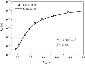
Figure 2. The calibrated transfer characteristics of the JL FinFET in this work compared with Guin et al [18]. Device parameters in table 1 are used.
Download figure:
Standard image High-resolution imageTable 1. 14 nm node device parameters used in simulations.
| Technology node | L (nm) | Wfin(nm) | Hfin(nm) | tox(nm) | Lext(nm) |
|---|---|---|---|---|---|
| 14 nm | 20 | 6.4 | 30 | 0.8 | 8 |
3. Simulation methodology
To analyze the statistics of variability sources, one can use hundreds of atomistic simulations for each random dopant or random metal grain profile [19]. However, full 3D calculation of atomistic simulations is computationally expensive. Hence, atomic simulations are not appropriate for statistical analyses that require multiple simulations. In addition, atomistic simulation can lead to severe deviation if mesh-sizes are not properly designed as pointed out by El Sayed et al [20].
On the other hand, the impedance field method (IFM) was first proposed by Mayergoyz and Andrei in 2001 [21]. The basic idea of the IFM is small signal analysis which means the treatment of randomness as a perturbation of the 'reference' device [17]. Assuming a linear response of the contact voltage or current to fluctuations, Green's functions are exploited to compute the current response. Compared to atomistic simulations, IFM has advantages for the statistical analysis of variability sources [17, 20]. First, IFM is computationally efficient since time-consuming 3D calculations are only performed once for the 'reference' structure. Current fluctuations from the perturbation of dopant or metal grain profiles are calculated based on linear response theory. Second, IFM can be applied not only to RDF but to geometric fluctuations such as OTV. For these reasons, IFM was chosen to analyze the variability of JL FinFETs in this work.
We investigated 1000 samples of different dopant or metal grain profiles and conducted statistical analyses for Vth and Ssub. For RDF, random dopants are assumed to follow a Poisson distribution and to be uncorrelated with each other. That is, the probability to find k dopants P(k) in the mesh box with volume V is [17]:
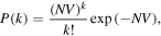
where N is an average doping concentration. For WFV, metal grain shapes and sizes are randomly generated. The only adjustable parameter in the simulations is AverageGrainSize which determines not only the average size of grains but also number of grains inside a metal electrode [17]. OTV is activated in simulations by correlating the oxide interface with the grains in the gate metal. The oxide interface shift between grains can be set by adjusting the displacement parameter amp [17]. Unless specified otherwise, AverageGrainSize is set to 5 nm according to the previous work [22, 23]. Also, amp is set to 0.2 nm since the atomic step at Si/SiO2 interface is 0.2 nm [24]. RDF and WFV are visualized by Sentaurus TCAD in figures 3(a) and (b), respectively. Perturbation of these dopant and grain profiles is calculated based on linear response theory and it only takes 2–3 times as long as a 'reference' simulation run [20]. More explanations on AverageGrainSize and amp and can be found on section 3.2.
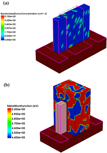
Figure 3. The simulated JL FinFET showing (a) RDF and (b) WFV. To visualize dopant distribution, gate metal and gate oxide region are hidden in (a).
Download figure:
Standard image High-resolution image3.1. Effects of doping concentration on variability
To investigate the effects of doping concentration on the variability, we simulated lightly doped (LD, ND = 2 × 1018 cm−3) and heavily doped (HD, ND = 1.4 × 1019 cm−3) JL FinFETs. To adjust that their off current to be the same, TiN and MoN were used as the gate metals for LD and HD devices, respectively. These gate metals are widely used in JL FinFETs, and their grain formations are well researched along with their grain orientations [22, 25]. Their work function values for different grain orientations are shown in table 2 with the effective work function WFeff [22, 25].
3.2. Effects of grain-related parameters on variability
As grain formulation is inherently random and undecidable, the grain-related parameters AverageGrainSize and amp need to be investigated for WFV and OTV induced variability. In 3D simulations, a 5 nm AverageGrainSize means the average grain sizes along the x, y, and z-axis are all 5 nm. After AverageGrainSize is specified, the average number of grains for the gate metal is determined. Then, grains are randomly generated in a Poisson distribution with an expected value equal to the average number of grains. As shown in figure 3(b), the grains can have various shapes and sizes. When OTV is specified in the simulation, a random number g is selected from the standard normal distribution for each grain. Then, the interface shift along the normal direction of the oxide interface is g multiplied by amp [15].
To analyze the effects of random grain formulation, AverageGrainSize and amp were individually varied from 1 nm to 30 nm, and from 0.2 nm to 0.6 nm, respectively [26].
3.3. Effects of device parameter scaling on variability
In sections 3.1 and 3.2, process variability was investigated when the average device parameters were fixed at the values in table 1. In this section, to investigate the most effective device parameter scaling on RDF, WFV, and OTV induced variability, we varied each of the device parameters: L, Wfin, Hfin, and tox. For the reference device parameters in table 1, ±10% variation for each parameter was assumed and their individual effects were compared. We defined the following parameters:


ΔσVth and ΔσSsub represent the effects of scaling of their corresponding device parameters on process variability. For example, if positive ΔσVth is observed for Wfin variation with RDF, it means Wfin scaling results in a reduction of σVth_RDF.
4. Results and discussion
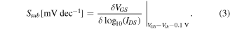
Two important subthreshold electrical parameters Vth and Ssub are extracted from the simulation results. Vth is defined as the corresponding gate voltage when the drain current reaches 10−7 A. Ssub is extracted at 0.1 V below Vth using the following equation:
4.1. Effects of doping concentration on variability
Figures 4(a) and (b) show the distributions of Vth and Ssub due to the combination of RDF, WFV, and OTV of generated 1000 samples for LD and HD devices. Although they have different doping concentrations, Vth shift is zero since their off current are adjusted to be the same by using different gate materials. It can be observed at a glance that HD JL FinFET is more prone to process variability than LD device. The combined effects of RDF, WFV, and OTV are analyzed by using σVth_SUM and σSsub_SUM [17]:


For further analysis, the extracted mean and standard deviation values of Vth and Ssub for each RDF, WFV, and OTV are shown in tables 3 and 4. Both σVth and σSsub values are greater in the HD JL FinFET for all variation sources including RDF, WFV, and OTV. RDF effects are more severe in HD than in LD JL FinFETs due to the average dopants difference in the channel region. The average dopants are estimated to be 7 and 53 for LD and HD devices, respectively. It has been seen that more in-channel dopants induce more variability [11].
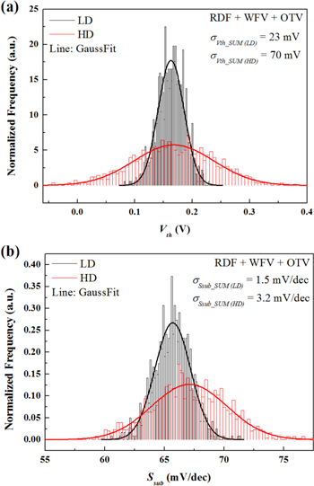
Figure 4. (a) Vth and (b) Ssub distributions of 1000 samples induced by combination of RDF, WFV, and OTV for LD and HD JL FinFETs.
Download figure:
Standard image High-resolution imageTable 3. Mean and standard deviation values of Vth due to RDF, WFV, and OTV for two different doping concentrations (LD: 2 × 1018 cm−3, HD: 1.4 × 1019 cm−3).
| μVth(V) | σVth_RDF(mV) | σVth_WFV(mV) | σVth_OTV(mV) | |
|---|---|---|---|---|
| LD | 0.17 | 16 | 16 | 1 |
| HD | 0.17 | 50 | 49 | 8 |
Table 4. Mean and standard deviation values of Ssub due to RDF, WFV, and OTV for two different doping concentrations (LD: 2 × 1018 cm−3, HD: 1.4 × 1019 cm−3).
| μSsub (mV dec−1) | σSsub_RDF (mV dec−1) | σSsub_WFV (mV dec−1) | σSsub_OTV (mV dec−1) | |
|---|---|---|---|---|
| LD | 65.7 | 1.2 | 0.9 | 0.2 |
| HD | 67.2 | 2.5 | 2.0 | 0.3 |
WFV induced variability was also higher in HD than LD devices. As shown in table 2, the work function difference for 〈200〉 and 〈111〉 of TiN (0.2 eV) is less than that for 〈110〉 and 〈112〉 of MoN (0.6 eV). Due to the large work function difference of MoN in HD JL FinFETs, WFV induced variability is larger in HD devices. It can be inferred that the appropriate choice of gate metal to meet a Vth target is one of the ways to reduce variability.
For OTV, HD JL FinFETs have a higher σVth than LD devices. In JL FinFETs, the electric field applied by a gate on the oxide and channel region depends on the channel doping concentration. Due to the high doping concentration of the channel in these FinFETs, the electric field applied to the oxide region is greater than in LD devices [27]. Hence, variability induced by OTV is greater in HD JL FinFETs. However, compared to the ΔσVth and ΔσSsub induced by RDF and WFV, OTV induced variability is negligible.
4.2. Effects of grain-related parameters on variability
Figures 5(a) and (b) show the extracted σVth and σSsub of HD JL FinFETs with varied AverageGrainSize. The figures can be exploited to determine minimum average grain size when the variation limit is chosen in 14 nm node JL FinFET by using (4) and (5). As expected, RDF has nothing to do with AverageGrainSize since RDF has no correlation with this parameter. It is shown that σVth_WFV and σVth_OTV increase as AverageGrainSize. The results are obvious since the average number of grains decreases as AverageGrainSize increases. σSsub_WFV and σSsub_OTV also increase as AverageGrainSize increases. Interestingly, however, σSsub_WFV starts to decrease when AverageGrainSize exceeds 15 nm.
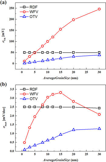
Figure 5. The AverageGrainSize parameter dependence of (a) σVth and (b) σSsub induced by RDF, WFV, and OTV.
Download figure:
Standard image High-resolution imageTo investigate the effects of AverageGrainSize on WFV in detail, the distributions of Vth and Ssub for 1000 samples are shown for different values of AverageGrainSize in figures 6 and 7. When AverageGrainSize is 5 nm, Vth and Ssub follow Gaussian distribution with a mean value of 0.17 V and 67.2 mV dec−1, respectively. Until AverageGrainSize reaches 15 nm, the decrease in the average number of grains is responsible for the increase of σVth_WFV and σSsub_WFV as shown in figures 6(a), (b), 7(a), and (b). When AverageGrainSize exceeds 15 nm, the distributions are no longer Gaussian distribution. This is because the grain sizes of the gate metal are comparable to the gate size, which means the gate metal is made up of only a few grains. Then, the effective work function of the gate metal is determined as either 4.4 eV or 5.0 eV, which results in Vth values of either −0.19 V or 0.41 V as shown in figure 5(c). Meanwhile, the distribution of Ssub is concentrated near its mean value (67.2 mV dec−1) when AverageGrainSize exceeds 15 nm. The Ssub value depends not on the effective work function value but on the distribution of grains in the gate metal. For an AverageGrainSize over 15 nm, one of the two different grain orientations govern the gate metal which is why σSsub_WFV decreases beyond this point in figure 6(b). It can be inferred that an increase of grain size to the level of gate size results in a severe degradation of Vth variation while Ssub variation shows relaxation. In addition, it should be noted that the position of grain boundary can be another factor that impacts on the subthreshold characteristics.

Figure 6. Vth distributions of HD JL FinFETs due to WFV when AverageGrainSize value is (a) 5 nm, (b) 15 nm, and (c) 30 nm, respectively.
Download figure:
Standard image High-resolution image
Figure 7. Ssub distributions of HD JL FinFETs due to WFV when AverageGrainSize value is (a) 5 nm, (b) 15 nm, and (c) 30 nm, respectively.
Download figure:
Standard image High-resolution imageThe effects of amp are visualized in figure 8 which shows that σVth_OTV and σSsub_OTV increase linearly as amp increases. In [28], OTV was found to be the most significant source of variability in IM FinFETs. In JL FinFETs, however, OTV is not as important as it is in IM FinFETs. Since the current in JL FinFETs conducts throughout the volume of the fin, carriers suffer less surface scattering. Hence, it can be concluded that OTV is not an important source of variability in JL FinFETs compared to RDF or WFV.

Figure 8. The amp parameter dependence of σVth (black square) and σSsub (red circle) induced by OTV.
Download figure:
Standard image High-resolution image4.3. Effects of device parameter scaling on variability
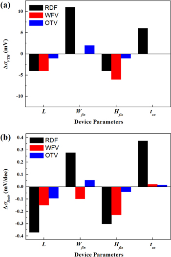
Figures 9(a) and (b) show the extracted ΔσVth and ΔσSsub after ±10% variation of L, Wfin, Hfin, and tox in HD JL FinFET. Note that the scaling factor of tox would be less than those of L, Wfin, and Hfin in the real technology nodes.
Figure 9. (a) ΔσVth and (b) ΔσSsub after ±10% of device parameter variation. Note that a positive value of ΔσVth or ΔσSsub means that device scaling of the corresponding parameter leads to a reduction of σVth or σSsub.
Download figure:
Standard image High-resolution image
For RDF, L and Hfin scaling increases σVth_RDF and σSsub_RDF while Wfin and tox scaling decreases them. Since RDF is correlated with channel size, scaling of L and Hfin leads to degradation of variability. On the other hand, improvement of gate controllability by Wfin and tox scaling reduces Vth and Ssub variability.
The effects of device parameters on WFV induced variability are generally less than their effects on RDF induced variability. σVth_WFV is correlated with the gate size which determines the number of grains in the gate metal. σVth_WFV is aggravated as L and Hfin decrease due to the reduction of grains. Although Wfin is related to the gate size, its effect is negligible since AverageGrainSize is 5 nm, comparable to 6.4 nm of Wfin. In addition, since Wfin and tox have a negligible impact on σVth_WFV and σSsub_WFV, it can be inferred that WFV induced variability is more closely correlated with gate size by L and Hfin than it is with gate controllability by Wfin and tox.
As indicated in section 4.2, OTV is not a significant source of variability in JL FinFETs. It is also shown in figures 9(a) and (b) that OTV has less impact than RDF or WFV on σVth and σSsub with device parameter variations.
In summary, RDF is the source of variability most sensitive to device scaling. Within ± 10% variations, the device parameter which results in the most severe fluctuation of σVth is Wfin, whereas L and tox have the most effect on the fluctuation of σSsub.
5. Conclusion
In this paper, variability analyses of 14 nm node JL FinFETs due to RDF, WFV, and OTV have been performed using the IFM. The effects of doping concentration, grain-related parameters, and device parameter scaling were studied by the standard deviation values of Vth and Ssub induced by RDF, WFV, and OTV.
Lightly doped JL FinFET with TiN gate was more stable than heavily doped device with MoN gate in all variability sources. As average grain size increases, WFV leads to greater degradation of ΔσVth and ΔσSsub than OTV does. Interestingly, WFV induced ΔσSsub shows marginal relaxation after average grain size is 15 nm. Minimum average grain size can be determined when the variation limit is chosen in 14 nm node JL FinFET. Our work also showed that RDF is the most severe source of variability as devices scale down. It has been observed that Wfin and tox scaling reduces RDF induced variability, whereas L and Hfin scaling increase RDF, WFV, and OTV induced variability.
The results reveal that the doping concentration of JL FinFETs must be low with an appropriate gate metal electrode to reduce variability. Also, grain size should be controlled considering the gate size. The impacts of each device parameter scaling should also be considered. Finally, this study's results can lead to a device design guideline for reducing device variability in JL FinFETs.
Acknowledgments
This work was supported by the Institute of BioMed-IT, Energy-IT and Smart-IT Technology (BEST), a Brain Korea 21 plus program, in Yonsei University. The EDA tool was supported by the IC Design Education Center (IDEC), Seoul, Korea.