
Abstract
The continuing miniaturization of optoelectronic devices, alongside the rise of electromagnetic metamaterials, poses an ongoing challenge to nanofabrication. With the increasing impracticality of quality control at a single-feature (-device) resolution, there is an increasing demand for array-based metrologies, where compliance to specifications can be monitored via signals arising from a multitude of features (devices). To this end, a square grid with quadratic sub-features is amongst the more common designs in nanotechnology (e.g. nanofishnets, nanoholes, nanopyramids, μLED arrays etc). The electrical resistivity of such a quadratic grid may be essential to its functionality; it can also be used to characterize the critical dimensions of the periodic features. While the problem of the effective electrical resistivity ρeff of a thin sheet with resistivity ρ1, hosting a doubly-periodic array of oriented square inclusions with resistivity ρ2, has been treated before (Obnosov 1999 SIAM J. Appl. Math. 59 1267–87), a closed-form solution has been found for only one case, where the inclusion occupies c = 1/4 of the unit cell. Here we combine first-principle approximations, numerical modeling, and mathematical analysis to generalize ρeff for an arbitrary inclusion size (0 < c < 1). We find that in the range 0.01 ≤ c ≤ 0.99, ρeff may be approximated (to within <0.3% error with respect to finite element simulations) by: 
![$\alpha (c)=1+\tfrac{0.9707}{{\left[0.9193+{\left(\tfrac{c}{1-c}\right)}^{2.1261}\right]}^{0.4671}}.$](https://content.cld.iop.org/journals/0957-4484/32/18/185706/revision3/nanoabdbecieqn2.gif) whereby at the limiting cases of c → 0 and c → 1, α approaches asymptotic values of α = 2.039 and α = 1/c − 1, respectively. The applicability of the approximation to considerably more complex structures, such as recursively-nested inclusions and/or nonplanar topologies, is demonstrated and discussed. While certainly not limited to, the theory is examined from within the scope of micro four-point probe (M4PP) metrology, which currently lacks data reduction schemes for periodic materials whose cell is smaller than the typical μm-scale M4PP footprint.
whereby at the limiting cases of c → 0 and c → 1, α approaches asymptotic values of α = 2.039 and α = 1/c − 1, respectively. The applicability of the approximation to considerably more complex structures, such as recursively-nested inclusions and/or nonplanar topologies, is demonstrated and discussed. While certainly not limited to, the theory is examined from within the scope of micro four-point probe (M4PP) metrology, which currently lacks data reduction schemes for periodic materials whose cell is smaller than the typical μm-scale M4PP footprint.
Export citation and abstract BibTeX RIS

Original content from this work may be used under the terms of the Creative Commons Attribution 4.0 licence. Any further distribution of this work must maintain attribution to the author(s) and the title of the work, journal citation and DOI.
1. Introduction
1.1. Target materials and their effective transport parameters
Square tessellation, i.e. a two-dimensional repetition of a square unit cell across the plane, is amongst the most straightforward engineering designs, naturally also found in nanofabrication. While hexagonal tiling is theoretically more efficient [1], and may exhibit marginally superior physical properties [e.g. 2], quadratic arrays with quadratic sub-features are often easier to manufacture and operate, as evidenced by their prevailing occurrence in micro-optoelectronic devices and electromagnetic metamaterial applications [3–11]. The broad range of target materials considered in this paper includes various types of biosensors, plasmonic materials, and optoelectronic devices (figure 1), all of which can be modeled as bi- or multi-composites as follows. The simplest imaginable bi-composite lies on the nanohole-nanofishnet continuum (figures 1(a)–(c)), where a uniform thin film (material 1) is perforated by square holes, constant both in size and spatial offsets with respect to one another (material 2 is void). A more sophisticated bi-composite results from filling that void with a different material, termed an inclusion (e.g. nanopatches in figure 1(d)). Planar multi-composites may be formed by the recursive nesting of inclusions within inclusions (e.g. single and double split-ring resonators in figures 1(e)–(f), respectively). Eventually, considerable complexity can be achieved by warping either the nanohole or the nanopatch arrays into the third dimension (e.g. nanowell/nanopyramid arrays in figures 1(g)–(h), and μLED array in figure 1(i), respectively). Since the electrical properties of all the abovementioned structures may be of key importance to their proper functioning, the premise of this paper is to make this broad range of materials and structures amenable to the theory of effective electrical transport, briefly outlined below.
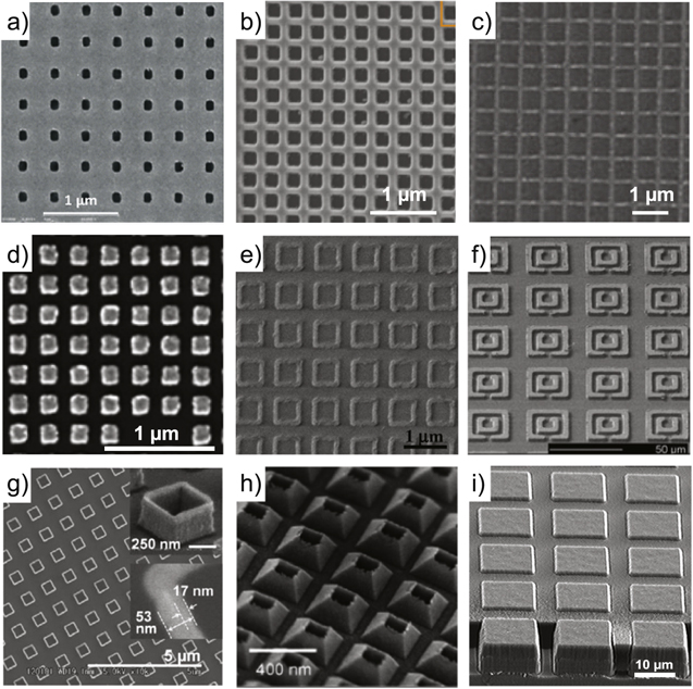
Figure 1. Nanostructures amenable to the hereby presented theory include, among others: (a) nanohole arrays [3], (b)–(c) fishnets [4, 5], (d) plasmonic nanoarrays [6], (e)–(f) single and double split-ring resonators [7, 8], (g) biosensor nanowells [9], (h) nanopyramids [10], and (i) μLED arrays [11]. Image credits: (a) reproduced with permission of The Royal Society of Chemistry; (b) © American Physical Society; (c) CC BY 3.0; (d) reproduced with permission of The Royal Society of Chemistry; (e) © IOP Publishing Ltd; (f) reprinted with permission from AAAS; (g) CC BY 4.0; (h) © American Chemical Society; (i) reprinted by permission from Springer Nature.
Download figure:
Standard image High-resolution imageMost of the modern treatment of effective transport through composite media is due to Lord Rayleigh, who in 1892 considered the effects of circular or spherical inclusions of resistivity ρ2, periodically embedded within a host medium of resistivity ρ1 [12]. Serving the 1960s boom of microfabrication, further seminal theory was developed by Keller [13] and later Dykhne [14], who proved that the effective sheet resistance of an infinite (and possibly random) planar checkerboard bi-composite obeys ρeff =  The seminal mathematical analysis of effective transport in a bi-composite with oriented square inclusions [15] (i.e. inclusions aligned in parallel to the principal axes of the square unit cell), appears to be due to Mortola and Stefeé [16]. A decade and a half later, one of their conjectures was rigorously proven by Obnosov [17], who introduced the variable transformation:

and expressed the effective resistivity of a doubly-periodic bi-composite, whose inclusions occupy precisely c = 1/4 of the unit cell, as:

In order to appreciate equation (2), its key behavior and selected assumptions [17] are visualized in figure 2. The square unit cell (figure 2(a)) consists of a thin sheet, composed of two media with isotropic resistivities ρ1 (host) and ρ2 (inclusion), c being the fractional area of the inclusion in the unit cell. In the analytical solution for c = 1/4, the effective resistance (equation (1), figure 2(b)) varies between ρ1/ to
to  ρ1 for ρ2 ≪ ρ1 and ρ1 ≪ ρ2, respectively. Note, that the response is symmetric about ρ2 = ρ1 [13], and that the factor
  is purely geometric [17]. Three representative scenarios in figure 2(b) are further shown in figures 2(c)–(e), visualizing the preferential current flow in the low-resistivity medium (black arrows, with size proportional to current density), alongside equipotential lines (grey contours, 0.05 V apart).

Figure 2. (a) Unit cell, with a centered square inclusion (shaded), occupying a fractional area of c. (b) Equation (1), predicting scaled effective resistivity ρeff as a function of ρ2/ρ1 for c = 1/4. (c)–(e) Finite element modeling of three scenarios (marked as circles in (b)), showing current flow lines (black arrows) and equipotential contours (grey lines, 0.05 V apart); model assumes c = 0.25, sheet resistance ρ1/d = 1 kΩ, and I = 1 mA.
Download figure:
Standard image High-resolution image1.2. Four terminal sensing of a doubly-periodic array of square inclusions
Micro four-point probe (M4PP) metrology is a well-established electrical technique, which enables measurement of key electrical material properties (e.g. sheet resistance or resistivity, carrier density and mobility, tunneling magnetoresistance, etc) on micrometer length scales [18, 19]. Given that the spatial resolution of the technique scales with the electrode pitch, sub-pitch resolution can be difficult to obtain [20]. For example, it has been shown that spatial variations in sheet resistance can be mapped reliably only when the spatial extent of such variations exceeds probe pitch by at least an order of magnitude [21]. Sub-pitch resolution may arguably be attained by deconvolution of data from a dense areal sampling [22]; however, this involves non-unique inversion of an underdetermined system, and thus is applicable only for simple (e.g. quasi-1D) patterns. Although recent theoretical progress has enabled accurate M4PP measurements of small pads with dimensions barely in excess of the M4PP probe footprint [23, 24], there is still a clear lack of M4PP methodology for smaller (i.e. sub-pitch) motif sizes. Motivated to close this gap, the current study devises a data reduction scheme for accurate M4PP metrology of electrical transport in doubly-periodic bi- or multi-composites with sub-pitch periodicity.
To verify that equation (2) remains valid also for M4PP measurements, where the electrical current propagates in a markedly different manner to what is modeled in figure 2, we undertook a full-scale M4PP simulation (figure 3) via finite element modeling (FEM) using COMSOL 5.5 [25]. Over a large 59 × 59 square matrix of bordering unit cells, a four-point resistance measurement is simulated via four collinear and equidistant circular contacts of radius r0, where current is passed between two contacts and the voltage drop is registered by the remaining two (figure 3(a)). From the 4! = 24 combinations of electric terminal assignment to the four electrodes (I+, V+, V− and I−), we simulate only the three baseline configurations [18]; the resulting dual-configuration sheet resistances [18] are numerically indistinguishable, regardless of the chosen configuration pair.

Figure 3. (a) Three possible arrangements ('+', 'x', 'o') of an equidistant collinear M4PP probe with pitch p on top of a doubly-periodic square composite (unit cell size of a and c = 1/4), (b) dual-configuration resistivity ρeff from M4PP simulations (further scaled by ρ1) as a function of ρ2/ρ1 (symbols match those in subplot (a)), overlain by theoretical expectation from equation (2) (continuous curve). (c) Relative error of simulated dual-configuration M4PP measurements from theory (equation (2)).
Download figure:
Standard image High-resolution imageThe numerically simulated ρeff/ρ1 as a function of ρ2/ρ1 (symbols in figure 3(b)) match theory (solid line in figure 3(b)) to within a few percent (figure 3(c)) and thus confirm the relevance of equation (2) for M4PP array-metrology. The deviations in figure 3(c) arise not from numerical artefacts (which are <0.017% as will be shown in section 2.3), but mainly from the M4PP method itself (i.e. a finite electrical contact size r0, and the position of each contact with respect to inclusions). Nevertheless, even for a probe whose pitch is only marginally larger (factor 1.24) than the unit cell size (circles in figures 3(a)–(c)), these deviations clearly remain second-order effects, overlain on top of an otherwise well-behaved theoretical trend (equation (2)). At this point, we can conclude that while equation (2) seems readily applicable to M4PP array-metrology, its inherent geometric constraint (c = 1/4) is specific, and is of limited practical use. However, anticipating that the symmetry of equation (2) may extend to other inclusion sizes, we take a more in-depth look at a single unit cell, as shown next.
2. Models
2.1. First-principles approximation
For the rigorous mathematical derivation of equation (2), applicable only for c = 0.25, the reader is referred to [17]. Since from a mathematical standpoint, a closed-form analytical solution for c ≠ 0.25 seems improbable [26], here we resort to physical first principles, and make simplifying assumptions to obtain an approximate expression for ρeff for arbitrary values of c. To further generalize the treatment, in all our subsequent algebra we operate with isotropic sheet resistances R = ρ/d, i.e. resistivities ρ scaled by their corresponding materials' thicknesses d. This makes composites, whose components might have different thicknesses (all negligible in comparison to the M4PP probe pitch), amenable to the very same treatment.
Let the periodic array have a unit cell of size a × a, with a centered square inclusion of size  ×
×  as before. When electrical current is forced across the unit cell from its left to its right edge (figures 2(a) and 4(a)), the vertical edges are potential lines, while the horizontal edges are flux lines. Due to symmetry, the bisecting vertical and horizontal lines through the unit cell are also potential and flux lines, respectively; thus, all further treatment can be reduced to a single quadrant of the unit cell (e.g. its lower right quarter in figure 4(a)). The host and inclusion materials have sheet resistances R1 and R2, respectively. We now recast the problem into a resistor network, under two complementary assumptions. In the first, all equipotential lines through the quadrant are taken to be approximately vertical, and thus the effective resistance can be calculated from a simple network with two parallel resistors in series with a third resistor (figure 4(b)):

Figure 4. (a) The unit cell from figure 1(a), subdivided into quadrants with sheet resistance R1 and R2 (see text). (b)–(c) Two alternative arrangements of the lower right quadrant of the unit cell into a linear resistor network (equations (3)–(4), correspondingly), each resistance weighted by the width/height ratio of its corresponding rectangle. (d) Comparison of equation (5) with finite element model simulations, for several representative values of c. (e) The maximum relative error of equations (3)–(5) with reference to the FEM simulations (0.017% is the threshold for numerical artefacts; see text).
Download figure:
Standard image High-resolution imageUnder the alternative assumption, all flux lines are taken to be longitudinal, and thus the effective resistance can be calculated by considering two series resistors in parallel with a third resistor (figure 4(c)):
Although neither of equations (3)–(4) is accurate, a more adequate description of the effective current distribution in the plane may be obtained if we imagine an infinite (and possibly random) checkerboard of quadrants, each of which obeys either equation (3) or (4). Using Dykhne's formalism [14], we take the geometric mean of equations (3)–(4) and obtain:
where  and
and  Such spatial averaging is valid if one imagines an electrical current spreading in 2D through many unit cells. As will be shown next, equation (5) performs equally well for even a single unit cell. At this point we note that equation (5) qualifies as a purely algebraic extension of equation (2), since it reduces to the latter for c = 1/4. To test the validity of equation (5) for other values of c, we compare it to finite element model simulations, as described next.
2.2. Numerical model
To test equation (5) against numerical results, FEM of electrical currents in a single unit cell were performed in COMSOL 5.5 [25]. Electrical currents of opposite signs flow in and out of the left and right edges of the unit cell, with voltage fixed to zero at its center. Solving for the electric field in steady-state, we divide the potential drop between the inlet and outlet current terminals by the current and sheet thickness to obtain the effective sheet resistance of the composite medium. The model was solved using a 'physics-controlled mesh' with 'extremely small' element size, corresponding to a Delaunay triangulation of ∼25000 elements, with an average element size ∼4.5 orders of magnitude smaller than the unit cell. To verify the universality of the results, we operated on non-dimensionalised variables, testing the response of Reff/R1 as a function of R2/R1 for a range of varying unit cell dimensions (size and thickness), absolute sheet resistances (R1 and R2), and current intensities (I), all of which had no numerical effect on the results. At the next step, the nondimensional variables of interest were varied from c = 0.01 to c = 0.99 (step of 0.01), and R2/R1 from 10−6 to 106 (10 steps per decade).
Predictions of equation (5) for a few representative values of c (red curves in figure 4(d)) are overlain by corresponding FEM simulations (dots), showing good agreement over a wide range of c and R2/R1. To quantify the error, figure 4(e) shows the maximum deviation of equations (3)–(5) with reference to the numerical model for all numerically simulated values of c. The approximations of either equations (3)–(4) lead to relative errors of up to 16%. In contrast, their geometrical mean (equation (5)) keeps the relative error under 5% over the entire range of c (figure 4(e)). Remembering that equation (5) with c = 0.25 is an exact solution, we can quantify the accuracy of the FEM model itself. For c = 0.25, the maximum relative error of the simulated Reff/R1 ranged from 10−8 at R2 = R1, to a maximum of 0.017% at the scenario extremities R1≫R2 and R1≪R2. The latter figure (0.017%) is thus a representative value for error due to purely numerical artefacts.
2.3. Analytical approximation
Recognizing the power law in equation (2), we conjecture a purely algebraic generalization:

and hypothesize that the particular parameters for c = 1/4 (α = 2 and β = 1/2 in equation (2)) might be drawn from a broader continuum of values. As it turns out, the fit quality of equation (6) to the numerically simulated results is outstanding (figure 5(a)). The fact, that the maximum error of equation (6) is comparable to that of numerical artefacts (figure 5(b)), suggests that equation (6) may be generally valid also for c ≠ 0.25 (subject to proof, not attempted here). While the trends of α and β both appear smooth and continuous with respect to c (figure 5(c)), and are even strongly anticorrelated (Pearson's ρ = –0.84), the truly remarkable observation is that their ratio β/α is numerically indistinguishable from c (figure 5(d)). Utilizing the discovered relationship β = αc to get rid of β, we rewrite equation (6) as:

and proceed to investigate whether the relationship between α and c is also amenable to parameterization.
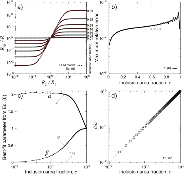
Figure 5. (a) Simulated Reff/R1 for several representative values of c, and best fits of equation (6). (b) The maximum relative error of equation (6) as a function of c. (c)–(d) The best fitting parameters from equation (6), both individually (c) and as a ratio (d).
Download figure:
Standard image High-resolution imageAfter some trial and error, a plausible relationship emerges between the transformed parameters α' = α – 1 and c' = c/(1 − c) (figure 6(a)), wherein α' approaches a horizontal asymptote for c' → 0, and α'→1/c' for c'→∞. This suggests a hyperbolic relationship of the form α' ∼ 1/(1 + c'), possibly requiring further modifications to achieve a smooth transition between the two asymptotic behaviors. In particular, we find that:

yields excellent (R2 = 0.9997) fits to α as a function of c, such as the one shown in figure 6(b), for the particular coefficients of γ1 = 0.9499, γ2 = 0.8063, γ3 = 2.158, and γ4 = 0.4576. Aiming to minimize the maximum error of equation (7) across the entire FEM dataset (rather than the misfit of equation (8) to the bestfit values of α), we obtain slightly different coefficients γ1 through γ4, which results in:
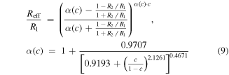
which is the core result of this work. Evaluating the goodness-of-fit of equation (9) to the FEM dataset, we find that within the range 0.01 ≤ c ≤ 0.99, equation (8) represents the FEM results with a maximum relative error of 0.3% (figure 6(d)). Note that the presence of four minima in the error of equation (8) (red curve in figure 6(d)) at c values of 0.01, 0.56, 0.87 and 0.98 arise from the four fitting parameters γ1 through γ4 in equation (8).
Figure 6. (a) The relationship between the transformed parameters α' = α − 1 and c' = c/(1 − c) is systematic, reminding a single branch of a hyperbola. (b) The relationship between c and the bestfit α from equation (7) (dots), empirically reproduced by equation (8) (curve). (c) Reff/R1 for representative values of c, functionally approximated via equation (9). (d) The maximum relative error of equation (7) with tabulated α (black curve; see appendix), and of equation (9) (red curve) for individual values of c.
Download figure:
Standard image High-resolution image3. Extended applications
3.1. Nested structures
As with Kirchhoff's circuit law, which can be iteratively applied on subsets of a linear resistor network, we hypothesize that equation (9) may be similarly used to predict the behavior of a nested system of square inclusions. We expect that this should be possible via a recursive application of equation (9), further shorthanded as f(c, R2/R1), from the innermost to the outermost inclusions. For simplicity, we constrain ourselves to two materials R1 and R2 as before, progressively nesting them within one another (bottom right of figure 7). Alongside a simple square inclusion as already treated before (equation (10a )), we consider a single (equation (10b )) and a double (equation (10c )) square ring inclusion, writing the corresponding recursion as:


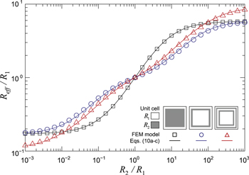
Figure 7. Comparison of a single-inclusion behavior (squares) with two exemplary systems with nested inclusions (circles and triangles). Inset: the corresponding unit cells defined by equation (10).
Download figure:
Standard image High-resolution imageThe predictions of equation (9a )–(9c ) are plotted as continuous curves in figure 7. After confirming that the theoretical behavior of nested inclusions discernibly diverges from that of a single-inclusion system, we proceeded to examine our theoretical predictions against a numerical simulation (symbols in figure 7). The match between theory and simulation in figure 7 confirms our hypothesis that equation (9) can be used recursively to predict the behavior of arbitrarily complex hierarchies of nested square inclusions, granted that they are all oriented and centered within each other. At this point, it is also important to note that since the approximation errors of the nested instances of equation (9) may be multiplicative, caution must be taken with increasing recusion depth.
3.2. Three-dimensional structures
Although the ability to model the effective resistivity of planar square grids is important, an increasing number of thin film devices involve out-of-plane nanostructuring in order to attain certain functionalities (e.g. flexibility in particular). An example of a doubly-periodic non-planar array of hollow frustums (lacking their base faces, but interconnected through their edges), whose top and side faces may have different electric properties, is shown in figure 8(a), alongside four M4PP electrodes probing that surface (to approximate scale; cf. figure 3(a)). Since current can flow only at the surface of the target structure, it is reasonable to assume that the problem of effective sheet resistance in figure 8(a) can be reduced to an equivalent 2D problem via conformal mapping [27]. Since the latter is angle-preserving, all the core mathematical description of the electrical field will be retained (i.e. derivatives and gradients) on an equivalent and simpler topology.

Figure 8. (a) Four terminal sensing of a non-planar, doubly-periodic thin film, approximating a matrix of interconnected hollow frustums. (b) A progression of frustums with height/base ratios varying from 0.1 to 1; the inclusion area is marked in grey, and the fractional area c quoted below each shape. (c) A quasi-conformal mapping of the frustums in (b) onto a planar square cell, with the transformed fractional area c quoted below each shape as in (b). (d) Comparison of direct FEM simulations of frustum effective sheet resistance (squares), versus theoretical prediction from equation (9) with c estimated from the quasi-conformal mapping (continuous curves); FEM and theory diverge by not more than 12% (relative).
Download figure:
Standard image High-resolution image
To test this idea, a series of square truncated pyramids (frustums), with aspect ratios (height/base) ranging from 0.1 to 1, were constructed (figure 8(b)) and densely meshed via Delaunay triangulation (not shown). Each frustum is hollow, lacks its base face, and is a composite of medium R1 at its sidewalls (colored), and R2 at its top face (grey); the relative area of R2 with respect to the total surface area is quoted below each shape in figure 8(b). To avoid a rigorous mathematical treatment at this proof-of-concept stage, we resorted to a quasi-conformal mapping technique prevalent in image analysis, known as Teichmüller mapping, and used an openly-available algorithm [28] to project the dense frustum triangulations onto a planar unit square (figure 8(c)), whereon the relative area of R2 noticeably scales down (quoted below each shape in figure 8(c)). After verifying that the obtained angle distortions are small (0° ± 2.5°), we approximate c as the fractional area of R2 in the Teichmüller map, and use equation (9) to predict the effective resistivity of the composite non-planar bi-composite as a function of R2/R1 (continuous curves in figure 8(d)). The original 3D frustum is then subjected to a FEM resistivity simulation on a unit cell (as in section 2, only on 3D topology), and the results (square symbols in figure 8(d)) are overlain on the theoretical expectation.
The error of the theoretical expectation relative to actual FEM simulations is <12% for the shallowest frustum considered, and <0.3% for the tallest. A reasonable explanation for the progressive departure of analytics from numerics for the shallowest frustums is that their originally strictly square top faces become mildly rounded on a Teichmüller map, thereby ceasing to be 'square'. For the majority of the taller frustums though, the area of R2 in the Teichmüller map is so small that essentially it is indistinguishable from an equivalent square. However, a larger and non-square shape occupying the majority of the unit cell (e.g. two leftmost frustums in figures 8(b)–(c)) could appreciably affect the electric flow lines (see figures 2(c)–(e)), bringing about the observed departure of theory from simulations as observed in figure 8(d). While several other factors may be in play and should be considered (the accuracy of the Teichmüller mapping, and of the electric field simulation in 3D), a fractional error of <12% for a broad range of non-planar unit cell geometries appears quite promising, especially if it replaces a computationally-demanding numerical simulation with a robust semi-analytical approach. As a final remark, we mention that full-scale M4PP simulations, similar to those in section 2 yet on arrays of interconnected frustums, retain the same behavior as a single unit cell (figures 8(b), (d)), and thus strengthen the relevance of this approach for M4PP metrology as well.
4. Conclusions
The determination of the effective properties of composites continues to be an active and exciting area of research [15, 29, 30], particularly when single-feature (or single-device) metrology at the nanoscale becomes physically-improbable [31]. Our present work extends a former treatment of effective resistivity in square arrays of quadratic inclusions [17] to arbitrarily-sized inclusions. Apart from equation (9), which is a surprisingly compact and accurate generalization of [17], we have also devised calculation schemes for recursively-nested inclusions, and non-planar topologies. The maximum error of our obtained approximation (0.3%) is comparable to the current best-case reproducibility of M4PP measurements on advanced thin film material stacks [32]. Should the need for higher accuracy arise, the interpolation of tabulated values of α(c) (appendix) reduces the maximum error of equation (9) to 0.03%. As evident from our analysis, other variables related to the M4PP method may superpose a few additional percent deviation from the theoretical predictions [33], thus making equation (9) satisfactory for any basic data reduction in M4PP array-metrology. While an analogous treatment for hexagonal arrays (e.g. graphene nanomesh devices [34]) is easily conceivable, this remains outside of the scope of the present study.
While any theoretical inference from numerical simulations should be treated with caution, the empirically discovered relationship in equation (7) is unequivocal: the effective resistivity in doubly-periodic array of oriented square inclusions follows a power law, whose exponent is proportional to the inclusion's fractional area. Equation (7) remains a conjecture, which we hope could turn useful for a more rigorous analysis, as has already occurred in this field before [15]. As electronic devices and interconnects continue to shrink, the extraction of accurate and statistically robust information from a given array of devices is of extreme importance in nanofabrication [31]. We are thus hopeful that our current work extends the M4PP application portfolio to a broader set of materials and structures characterized by double periodicity, where the unit cell size may be (considerably) smaller than the M4PP footprint.
Acknowledgments
This work has been supported by grants 8054-00020B (Denmark's Innovation Fund) and 8048-00088B Sapere Aude (Independent Research Fund Denmark). BG is grateful to Yurii Obnosov for discussions on extending his seminal 1999 treatment, and to Frederik Østerberg, Lior Shiv, Kristoffer Kalhauge, Rong Lin, and Yakov Guralnik for feedback on work in progress.
Comment added in proof
In a L'esprit de l'escalier of sorts, we have noticed that by defining Δeff = (1 – Reff
/R1)/(1 + Reff
/R1) (see equation (2)), a strikingly linear relationship Δeff
 cΔ is observed. Rearranging the latter, we obtain Reff
/R1 = (1 – cΔ)/(1 + cΔ), which does not only surpass equation (5) by brevity, but which is also marginally more accurate (<4.8% error for any c), thus probably qualifying as the best back-of-the-envelope calculation scheme to date.
cΔ is observed. Rearranging the latter, we obtain Reff
/R1 = (1 – cΔ)/(1 + cΔ), which does not only surpass equation (5) by brevity, but which is also marginally more accurate (<4.8% error for any c), thus probably qualifying as the best back-of-the-envelope calculation scheme to date.
Appendix
Tabulated values of α(c).
| c | α(c) | c | α(c) | c | α(c) | c | α(c) | c | α(c) |
|---|---|---|---|---|---|---|---|---|---|
| 0.01 | 2.038 85 | 0.21 | 2.016 66 | 0.41 | 1.855 14 | 0.61 | 1.537 41 | 0.81 | 1.224 74 |
| 0.02 | 2.038 70 | 0.22 | 2.013 12 | 0.42 | 1.841 85 | 0.62 | 1.520 46 | 0.82 | 1.211 07 |
| 0.03 | 2.038 52 | 0.23 | 2.009 18 | 0.43 | 1.828 12 | 0.63 | 1.503 58 | 0.83 | 1.197 62 |
| 0.04 | 2.038 45 | 0.24 | 2.004 82 | 0.44 | 1.814 00 | 0.64 | 1.486 78 | 0.84 | 1.184 37 |
| 0.05 | 2.038 21 | 0.25 | 2.000 03 | 0.45 | 1.799 50 | 0.65 | 1.470 08 | 0.85 | 1.171 34 |
| 0.06 | 2.037 98 | 0.26 | 1.994 78 | 0.46 | 1.784 64 | 0.66 | 1.453 49 | 0.86 | 1.158 51 |
| 0.07 | 2.037 67 | 0.27 | 1.989 06 | 0.47 | 1.769 45 | 0.67 | 1.437 03 | 0.87 | 1.145 90 |
| 0.08 | 2.037 26 | 0.28 | 1.982 85 | 0.48 | 1.753 96 | 0.68 | 1.420 71 | 0.88 | 1.133 49 |
| 0.09 | 2.036 81 | 0.29 | 1.976 15 | 0.49 | 1.738 19 | 0.69 | 1.404 54 | 0.89 | 1.121 29 |
| 0.10 | 2.036 21 | 0.30 | 1.968 93 | 0.50 | 1.722 18 | 0.70 | 1.388 52 | 0.90 | 1.109 28 |
| 0.11 | 2.035 50 | 0.31 | 1.961 19 | 0.51 | 1.705 95 | 0.71 | 1.372 68 | 0.91 | 1.097 49 |
| 0.12 | 2.034 61 | 0.32 | 1.952 92 | 0.52 | 1.689 52 | 0.72 | 1.357 01 | 0.92 | 1.085 89 |
| 0.13 | 2.033 59 | 0.33 | 1.944 13 | 0.53 | 1.672 94 | 0.73 | 1.341 52 | 0.93 | 1.074 49 |
| 0.14 | 2.032 35 | 0.34 | 1.934 80 | 0.54 | 1.656 21 | 0.74 | 1.326 22 | 0.94 | 1.063 28 |
| 0.15 | 2.030 93 | 0.35 | 1.924 95 | 0.55 | 1.639 38 | 0.75 | 1.311 11 | 0.95 | 1.052 27 |
| 0.16 | 2.029 27 | 0.36 | 1.914 57 | 0.56 | 1.622 46 | 0.76 | 1.296 20 | 0.96 | 1.041 45 |
| 0.17 | 2.027 34 | 0.37 | 1.903 68 | 0.57 | 1.605 47 | 0.77 | 1.281 50 | 0.97 | 1.030 81 |
| 0.18 | 2.025 15 | 0.38 | 1.892 27 | 0.58 | 1.588 46 | 0.78 | 1.266 99 | 0.98 | 1.020 36 |
| 0.19 | 2.022 66 | 0.39 | 1.880 37 | 0.59 | 1.571 42 | 0.79 | 1.252 70 | 0.99 | 1.010 09 |
| 0.20 | 2.019 84 | 0.40 | 1.867 99 | 0.60 | 1.554 40 | 0.80 | 1.238 61 |
* Within the tabulated range, α may be linearly interpolated; outside this range, use α = 2.039 for c < 0.01, and α = (1 − c)/c for c > 0.99.