

Abstract
The preparation of non-oxidized Ge quantum dot (QD) lattices embedded in Al2O3, Si3N4, SiC matrices by self-assembled growth was studied. The materials were produced by magnetron sputtering deposition, using different substrate temperatures. The deposition regimes leading to the self-assembled growth type and the formation of three-dimensionally ordered Ge QD lattices in different matrices were investigated and determined. The oxidation of the Ge QDs in different matrices was monitored and the best conditions for the production of non-oxidized Ge QDs were found. The optical properties of the Ge QD lattices in different matrices show a strong dependence on the Ge oxidation and the matrix type.
Export citation and abstract BibTeX RIS
1. Introduction
Semiconductor nanoparticles and quantum dots (QDs) have been studied extensively because of the possibility to tune the bandgap with the QD size, which makes them interesting for the application in photovoltaics [1–5]. Especially, silicon nanocrystal superlattices surrounded by different matrices were investigated for the top absorber material in all-silicon tandem solar cells [6]. The downside of such superlattices, among others, is that annealing temperatures up to 1000 °C or 1100 °C are needed for the silicon to crystallize [6–9]. In contrast Ge QDs are crystalline after annealing at 700 °C–800 °C [10–12]. Moreover, germanium has a larger exciton Bohr radius than silicon, so quantum confinement with Ge QDs is achieved for larger QD sizes. These properties make Ge an excellent material for many applications in modern nanotechnology. However, the critical issue for these applications is the presence of dangling bonds at the Ge QD/matrix interface [13–17]. This problem is especially present at the Ge/oxide interfaces. These interfaces usually have defect-related states with ps-ns response times and an enhanced radiative recombination of photo-generated carriers [15–17].
In our previous work, we have studied the preparation of Ge QD lattices in Al2O3 and SiO2 matrices produced by self-assembled growth during magnetron sputtering deposition [10, 11]. We also showed that it is possible to produce self-ordered core/shell Ge/Si QDs in an Al2O3 matrix [12, 18]. The self-assembled growth type enables the production of regularly 3D-ordered Ge QDs, i.e. the formation of QD lattices, with a narrower size distribution compared to the ones obtained by random growth regime, and it enables the control of the QD spacing which is important for various applications. The other important material parameter is the matrix in which the QDs are embedded. The matrix strongly influences the conductive properties of the material and the confinement effect. When an electron-hole pair is generated within a QD, the charge carriers should be separated before their recombination. If the conductivity of the matrix is low, and QDs are too far from each other, then the conductivity of the material is low and charge carriers cannot be separated [3, 19]. Therefore, an important property of the material containing QDs is their small separation which enables easy tunnelling of charge carriers, and the conductivity of the matrix which make tunnelling easier for a smaller bandgap value. Therefore, it is important to investigate the preparation of 3D Ge QD lattices in matrices other than alumina and silica, especially using the non-oxide ones. Ge QDs in non-oxide matrices were investigated by other authors [20, 21], however, a regular ordering of QDs has not been achieved in these films.
In this paper we investigate the self-assembled growth and the properties of Ge QD lattices in non-oxide matrices, thus we compare the structural properties and oxidation of Ge QDs in Al2O3, Si3N4, and SiC matrices. As a high-bandgap isolator, alumina presents a great matrix for obtaining strong quantum confinement, but for the same reason, the electric conductivity is poor. As explained above, for strongly non-conductive matrices QDs should be very close to each other for any photovoltaic application to be possible. [3, 19] On the other hand, silicon nitride and especially silicon carbide may have a weaker confinement but should have a higher conductivity, therefore presenting a promising substitute for alumina.
The produced films all have a separation between the QDs below or very close to 2 nm, and the Ge QDs in nitride matrix show strong confinement effects in accordance with the theory. The Ge QDs in alumina show strong oxidation which decreases significantly the absorption of this material. Finally, Ge QDs in SiC do not show confinement as expected, probably caused by the smallest bandgap value of the SiC matrix, but it shows strong absorption caused by the matrix. We demonstrate that non-oxide matrices strongly reduce Ge oxidation as expected, and we show a method how to reduce it also in an alumina matrix. After covering the Ge QDs with a protective Si layer, Ge is prevented from oxidation. Such QDs have a core/shell Ge/Si structure and they show a strong confinement and absorption peak in accordance with the theory related to QDs with Ge/Si core/shell structure [22].
2. Experimental
The investigated samples were produced by magnetron sputtering deposition using a KJLC CMS-18 system. The thin films are divided into three groups: the GA, GC and GN group, where the second letter denotes whether it is an aluminium oxide (A), silicon carbide (C) or a silicon nitride (N) matrix. Every group of samples was deposited on Si (100) substrates at temperatures of 300 °C, 400 °C, and 500 °C. An additional sample was produced by inserting a layer of Si over the Ge QDs with the aim to reduce Ge oxidation in the alumina matrix. Details about the deposition parameters of all samples and the Ge atomic percentage in the films are given in table 1. The base pressure in the chamber was 4.3 × 10⁻⁷ Pa, and the Ar pressure during all depositions was 0.47 Pa. The sputtering power for Ge and Si was 10 W and 50 W, respectively, and the powers for Al2O3, SiC and Si3N4 were 140 W, 300 W, and 125 W, respectively, in order to produce a similar deposition rate. Twenty bi-layers of Ge/matrix were produced. After the deposition, the films were annealed in vacuum (∼10–6 Pa) at 700 °C–900 °C with a duration of 45 min.
Table 1. Ge QD—based materials investigated in this work. The table contains the sample name, its composition related to the deposition method, deposition temperature (T), Ge atomic percentage in the films determined by ERDA—Ge (at%), and the parameters of the formed QD lattice: in plane separation of the QDs-a, the vertical separation-c and the average QD radius R, all parameter values are given in nm.
| Name | Composition | T (°C) | cGe (at%) | a | c | R |
|---|---|---|---|---|---|---|
| GA3 | Ge/Al2O3 | 300 | 13 | 3.8 | 2.4 | 1.0 |
| GA4 | Ge/Al2O3 | 400 | 13 | 3.8 | 2.1 | 1.3 |
| GA5 | Ge/Al2O3 | 500 | 13 | 4.8 | 2.1 | 1.3 |
| GA5Si | Ge/Si/Al2O3 | 500 | 9 | 6.7 | 3.9 | 1.6 |
| GN3 | Ge/Si3N4 | 300 | 14 | — | 2.2 | — |
| GN4 | Ge/Si3N4 | 400 | 14 | 3.5 | 2.4 | 1.0 |
| GN5 | Ge/Si3N4 | 500 | 12 | 3.8 | 2.5 | 1.2 |
| GC3 | Ge/SiC | 300 | 11 | 3.2 | 2.4 | 1.0 |
| GC4 | Ge/SiC | 400 | 11 | 3.7 | 2.7 | 1.1 |
| GC5 | Ge/SiC | 500 | 14 | 4.4 | 4.2 | 1.4 |
The ordering of QDs depending on the deposition parameters was investigated using the GISAXS (grazing incident small angle x-ray scattering) method. The crystalline structure of the films was simultaneously determined by GIWAXS (grazing incident wide angle x-ray scattering). The GISAXS and GIWAXS measurements were performed at the synchrotron Elettra, Trieste, Italy at the SAXS beamline, using a photon energy of 8 keV, and two separate 2D photon detectors (a Pilatus3 1M for GISAXS, and a Pilatus 100k for GIWAXS).
Selected samples were analysed using transmission electron microscopy (TEM) employing an image Cs-corrected Titan 80-300 microscope (FEI) operated at an accelerating voltage of 300 kV or a Talos F200X microscope (FEI) operated at 200 kV. In particular, atomic number contrast images were recorded in high-angle annular dark-field scanning TEM mode (HAADF-STEM).
Spectroscopic ellipsometry (SE) spectra were taken in the spectral range between 0.57 and 4.6 eV and angles of incidence of 65° and 75° with a J A Woollam V-VASE ellipsometer. Modelling of the SE data lead to the retrieval of the films effective thickness and dielectric function. The dependence of the optical constants of the films on the photon energy was represented with a multiple oscillator model that was able to account for the inter-band transition in QDs.
Photoemission spectra were recorded under UHV conditions (with a typical pressure in the 10−7 Pa range) using a SPECS XPS instrument, equipped with the Phoibos MCD 100 electron analyser and a monochromatized source of Al Kα x-rays of 1486.74 eV. For the pass energy of 10 eV used in the present study, the total energy resolution was around 0.8 eV. The experimental photoemission spectra were analysed by the Unifit software [23] and simulated with several sets of mixed Gaussian–Lorentzian functions with Shirley background subtraction. Before the XPS measurements, each sample was exposed to 2 keV Ar+ ion bombardment in order to remove surface contamination.
3. Structural properties
3.1. Ordering properties-preparation of QD lattices
In this section, we analyse the ordering properties of the formed Ge QDs in different matrices, i.e. the formation of 3D-ordered QD lattices.
In order to investigate how the matrix and the deposition temperature influence the QD ordering, we use the combination of the TEM and GISAXS techniques. TEM provides information in real space, while GISAXS shows the image in reciprocal space. Therefore, GISAXS is especially suitable for the analysis of 3D-ordered systems because the regularity in ordering causes strong Bragg spots in the GISAXS maps. From their arrangement in the GISAXS maps we can determine the ordering type and its quality (deviation from the ordering in an ideal lattice). Details about the determination of the structural parameters from GISAXS can be found in [24]. Using those models, we have determined the multilayer period c, the in-layer dot separation a and the QD radius R (table 1).
GISAXS maps of all films together with HAADF-STEM images of selected films are shown in figure 1. We can see that Ge QDs in alumina and silicon carbide form for all three deposition temperatures. For the nitride matrix, however, a deposition temperature of at least 400 °C is needed to induce QD formation during the film growth.
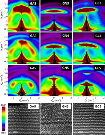
Figure 1. (a) GISAXS maps for all three sample sets. A, N and C denote the matrix type, specifically Al2O3, Si3N4 and SiC, respectively, while 3, 4 and 5 denote the deposition temperature, (300 °C, 400 °C and 500 °C, respectively). (b) The corresponding cross-sectional HAADF-STEM images for selected samples. The thin ring-like structure positioned near Qy = 3.3 nm−1 is an artefact of the measurement.
Download figure:
Standard image High-resolution imageThe self-organized growth of Ge QDs can be explained with a simple growth model [10, 11]. The combination of two mechanisms is influencing the growth: diffusion-mediated nucleation and an enhanced nucleation probability in the troughs of the underlying substrate. If diffusion-mediated nucleation would be the only growth mechanism, the result would be in-layer spatially correlated QD formation, with no interlayer correlations. Since the nucleation is more probable in the troughs of the previous layer, there will be a correlation in the QD position between the layers. The quality of ordering can be estimated from the width and intensity of the lateral Bragg spots. The most pronounced Bragg spots appeared for the deposition at 500 °C for all three matrices. Comparing different matrices, alumina shows the best ordering quality, while the nitride matrix is the worst (see figure 1(a))). HAADF-STEM images show similar results, where nice QD ordering is visible for the alumina and silica carbide matrices while for the silicon nitride matrix the regularity in ordering disappears after the first 10 layers.
The GISAXS map of the GA5Si film is shown in figure 2. For that film, a Ge/Si core/shell structure of QDs formed [18]. During the deposition, a thin Si layer is inserted after the deposition of each Ge layer. In that way, the Ge QD is prevented to be in contact with the oxide matrix. Instead, it is in touch with Si that has the same crystalline lattice and a similar lattice constant as Ge (the lattice constant of Si is about 0.96 times the lattice constant of Ge). Therefore, it should have less Ge oxide as will be shown in the following.

Figure 2. GISAXS map of Ge/Si/Al2O3 film, and a model of the Ge/Si core/shell QD.
Download figure:
Standard image High-resolution imageGISAXS maps of the films deposited at 500 °C and annealed after the deposition are shown in figure 3. Here we present only the data for the temperature at which the structure starts to change, and one temperature below (the temperatures changes in steps of 100 °C).
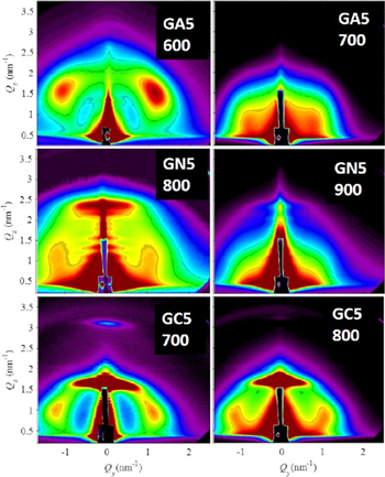
Figure 3. GISAXS maps of the selected annealed films. The annealing temperature (in °C) is indicated in the figure below the sample name.
Download figure:
Standard image High-resolution imageAs follows from the figure, the regular ordering of QDs starts to collapse at different temperatures. Thus, the disintegration of the QD lattice starts at 700 °C for the alumina matrix (GA5), 900 °C for the nitride matrix (GN5), while the same process occurs at 800 °C for Ge QDs in carbide (GC5).
The layered structure is still present at the mentioned limiting temperatures, but it is not the same as after the films growth. Increasing the annealing temperature, the disintegration propagates and results in a complete destruction of the film multilayer structure. This property is closely related to the crystallization temperature of Ge QDs as will be shown in the following subsection. We emphasize that the annealing is performed in steps of 100 °C, so we can determine here only the temperature range of 100 °C within which the change occurs.
3.2. Crystallisation properties
The crystalline properties were determined by GIWAXS measurements shown in figure 4. Generally, amorphous Ge shows two broad peaks in the measured angular range. After its crystallization the first Ge-related peak becomes narrower, while the second peak splits in two narrower peaks, (the Ge crystalline peaks are indicated by vertical dashed lines in figure 4).

Figure 4. GIWAXS 1D pattern of the investigated films annealed at different temperatures: Ge QDs in (a) Al2O3 matrix, (b) SiC matrix and (c) Si3N4 matrix. The dashed lines indicate the positions of the crystalline Ge peaks (111), (220) and (311). The annealing temperatures are indicated in panel (a).
Download figure:
Standard image High-resolution imageThe GIWAXS pattern of the as-grown films are shown by black lines in figure 4. All of them show only two broad peaks which correspond to amorphous Ge as explained above. There are no other peaks, so we conclude that both, Ge QDs and matrices are amorphous after the deposition of the films. That is accordance with our previous results obtained on Ge QDs in silica and alumina matrices produced by magnetron sputtering [10, 11]. However, the crystallization occurs at different temperatures for the three different matrices used in the present study. The lowest crystallization temperature was found for the alumina matrix (700 °C). For the carbide matrix Ge crystallizes at 800 °C, while Ge crystallizes at 900 °C in the nitride matrix. As was mentioned before, the GISAXS maps show the change for the temperatures that match the crystallization temperature of the Ge QDs. As follows from figure 3, this change occurs at 700 °C for alumina, 900 °C for nitride and 800 °C for the carbide matrix. Obviously, changes in the Ge crystalline structure also affect the ordering of Ge QDs.
The difference in crystallization temperature is not related to the QD size, because all Ge QDs investigated in the present study have a similar size. In addition, we have investigated Ge QDs with different sizes in alumina matrix, and they crystallize around 700 °C [10]. Ge QDs in silica matrix crystallize at 800 °C [11], while they crystallize already at 400 °C in conductive indium tin oxide (ITO) matrix [25, 26]. It is not clear why this large difference in crystallization temperature occurs, but the effect is evidently induced by the matrix type. The conductive ITO matrix has the lowest crystallization temperature, which indicates that the different crystallization temperatures could be related to the thermal properties of the matrices.
3.3. Oxidation properties
Turning now to the investigation of oxidation of Ge QDs caused by the matrix type, we stress once again that the oxidation of Ge QDs causes problems in the application of these materials. Oxidation of Ge QDs was studied by XPS, as shown in figure 5. We have monitored spectra around the Ge 2p3/2 and Ge 3d core-levels, exhibiting pronounced contributions of Ge oxides, characterized by characteristic peaks at higher binding energies (BE) compared to pure Ge. For example, in the spectrum around Ge 2p3/2 the GeO and GeO2 appear at the BE of 1218.1 eV and 1220.0 eV, respectively, while pure Ge is present at the characteristic BE of 1217.4 eV [27]. Similarly, in the spectra taken around the Ge 3d states, pure Ge is present at the characteristic BE of 29.5 eV, whereas the GeO and GeO2 peaks are shifted to the BE of 31.3 eV and 32.5 eV, respectively [28].
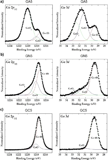
Figure 5. XPS spectra of the Ge QD-containing films in different matrices, measured around the Ge 2p3/2 and 3d states. (a) Al2O3 matrix, (b) Si3N4 matrix, (c) SiC matrix.
Download figure:
Standard image High-resolution imageThe presence of GeO and GeO2 is well pronounced in the XPS spectra taken from the Ge QDs in alumina matrix (figure 5(a)). In fact, the signal originating from the Ge oxides is much stronger than the Ge-related signal. The oxide contributions are significantly smaller for the nitride matrix, shown in figure 5(b), as the matrix contains no oxygen. A further reduction of oxide contribution is found in the SiC matrix, as shown in figure 5(c). The XPS measurements thus confirm the advantageous use of the non-oxide matrices for the preparation of Ge QD-containing materials.
The small amounts of oxide that are found in the films in non-oxide matrices obviously originate from the deposition chamber, although the base pressure was in the range of 10−7 Pa. It also shows that Ge QDs are indeed very sensitive to the presence of oxygen during the deposition, so even very small amounts of oxygen, present as residual gas in the chamber, incorporate in Ge QDs. Therefore, the Ge QDs in Al2O3 matrix are oxidized in a very large amount (over 80%).
However, it is also possible to prepare Ge QDs without oxidation in the alumina matrix. This is realized by adding a thin Si-layer after Ge deposition, as mentioned above (GA5Si film). The XPS measurements on this film are shown in figure 6. Ge-related oxides are not found in this film due to the deposition of the thin Si layer. But the Si layer itself is in contact with the oxide matrix, therefore it oxidizes. The XPS measurements of Si-related oxides are shown in figure 6(c). The Si shell indeed acts as a protective layer for Ge, but oxidizes itself, as evident from figure 6, where the SiOx and SiO2 signals (at the BE of 102.0 eV and 103.5 eV, respectively) are well developed in addition to the pure Si signal (at the BE of 99.5 eV), in full agreement with the literature [28].

Figure 6. XPS spectra of GA5Si film containing Si shells around the Ge QDs, measured around the Ge 2p3/2, 3d and Si 2p states.
Download figure:
Standard image High-resolution imageThus, to prepare oxygen-free Ge QDs, it is obviously necessary to cover the QD with some other material that will collect the oxygen and bond it to itself.
3.4. Optical properties
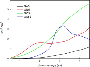
Finally, we present the optical properties of the films, and the influence of the matrix on the optical properties obtained from the measurements of the absorption coefficient α of different films, as shown in figure 7. If we consider Ge QDs without a protective shell (GA5, GC5 and GN5), then the Ge QDs in alumina matrix (GA5) show significantly lower absorption than the other two films. The absorption is strongest for the GC5 sample (SiC matrix). Only the film GN5 shows a clear absorption peak near 2 eV. The position of that peak is in accordance with the bandgap prediction for Ge QDs with a radius of 1.2 nm using the tight binding approximation [29]. The film GC5 has no clear peaks but it has the strongest absorption, while the film GA5 has the smallest absorption coefficient and also no visible peaks. We believe that the absence of visible peaks in the GC5 film (SiC matrix) is caused by the small value of the SiC matrix bandgap (3–3.5 eV), which affects significantly the confinement effects in Ge QDs, so we cannot apply a standard calculation which assumes an infinite bandgap (alumina has a bandgap above 7 eV). On the other hand, Ge QDs in alumina (GA5 film) are very strongly affected by the presence of oxide (see figure 5(a)), and therefore their absorption is strongly altered, so no peaks are visible. The film GC5 has the strongest absorption due to the SiC matrix, which has the highest extinction coefficient k, which is comparable to the values for Ge at energies above 2.5 eV (k is about 1.3 at 3 eV for SiC [30], while Si3N4 and Al2O3 have nearly k = 0.3 [31] and k = 0.01, respectively, for the same energy). Therefore, only the GN5 film shows a clear absorption peak with the position corresponding to the bandgap of Ge QDs with a radius of 1.2 nm.
Figure 7. Absorption properties of the films. Absorption coefficient α of Ge QDs in alumina, silicon carbide and silicon nitride matrices (GA5, GN5 and GC5), respectively. GA5Si contains Ge QDs with a protective Si layer on top in alumina matrix.
Download figure:
Standard image High-resolution image
The film containing a Si protective layer (GA5Si) has a relatively narrow absorption peak. The observed property is related to the core/shell Ge/Si structure of the QD. Such structure induces special effects including the appearance of strong absorption maxima, and therefore this film has different absorption properties than the pure Ge QDs which exist in the other three films investigated here [12, 18, 26]. This occurs due to the special confinement of carriers in such structures.
The theory describing the absorption properties of core/shell Ge/Si QDs is described nicely in [26]. The authors of that paper performed an ab initio investigation of the electronic structure of Si(core)/Ge(shell) and Ge(core)/Si(shell) core–shell nanocrystals, focusing on their excitonic properties. Their method is based on the density functional theory to obtain the single-particle states, which are used to calculate the excitonic properties within a configuration interaction framework. Due to the Ge-core Si-shell structure of nanocrystals, they exhibit type II band alignment in which the holes are localized in the Ge region, and electrons, in the Si region. The details of the calculation can be found in [26]. Regarding the presence of Ge-related oxides, GeO2 is a transparent material, with no absorption in the measured spectral range [32].
4. Conclusions
In this work we have investigated the formation of 3D-ordered Ge QD arrays in three different matrices, and the influence of the matrix on Ge oxidation and its optical properties. We have demonstrated the necessary conditions for the preparation of ordered Ge QD lattices in Al2O3, Si3N4 and SiC matrices. Ge QDs that form in non-oxide matrices have a significantly reduced amount of Ge-related oxides, which strongly enhances their light-absorption properties.
Acknowledgments
The authors are grateful to Joško Erceg for the help in the sample preparation and to Romy Aniol for TEM specimen preparation. NN, LB and MM acknowledge the Croatian Science Foundation (pr.no.2334), which supported this investigation. Support by the European Regional Development Fund for the 'Center of Excellence for Advanced Materials and Sensing Devices' (Grant No. KK.01.1.1.01.0001) and COST MuliScaleSolar project MP1406 is gratefully acknowledged. The use of the HZDR Ion Beam Center TEM facilities and the funding of TEM Talos by the German Federal Ministry of Education of Research (BMBF), Grant No. 03SF0451 in the framework of HEMCP are acknowledged. NN, LB and MM acknowledge the CERIC-ERIC Consortium for the access to the SAXS beamline and related financial support. IS and MP acknowledge the support of the University of Rijeka under the project number 18-144.