

Abstract
A systematic analysis of the electronic, thermoelectric and optical properties of triclinic van der Waal's solids NbX2Y2 (X = S, Se and Y = Cl, Br, I) is carried out within the framework of density functional theory for bulk and monolayer. The investigated compounds are semiconductors in bulk and monolayer, with band gap values ranging from 1.1 to 1.8 eV. We observed huge anisotropy in the electrical conductivity with the in-plane conductivity being 40 times higher than out-of-plane conductivity in NbS2I2. The observed high power factor and low thermal conductivity in NbX2Y2 render these compounds as potential thermoelectric materials. In addition, the calculated optical properties such as refractive index and absorption coefficient reveal the optical anisotropy. We have calculated birefringence for all the studied compounds and a large value of 0.313 is observed for NbSe2I2. The monolayer electronic properties indicate the presence of anomalous quantum confinement. The giant birefringence along with promosing monolayer properties are the highlights of present work which might fetch future device applications in both bulk as well as monolayer.
Export citation and abstract BibTeX RIS
1. Introduction
Materials with anisotropy in thermoelectric properties have been actively explored in recent years due to their novel applications [1–4]. Growing global population along with industrial growth lead to enhanced energy demands. Such an ever increasing demand for energy supply made us to look for alternative routes for energy harvesting without affecting our ecosystem. Thermoelectricity could be one of emerging technologies which paves the way to energy harvesting through conversion of heat into electricity and vice-versa. The efficiency of thermoelectric materials must be high for commercial use and characterized by a dimensionless quantity, figure of merit

where 'S' is thermopower, 'σ' is electrical conductivity, 'T' is temperature and 'kl' and 'ke' are the lattice and electronic contribution to the thermal conductivity respectively [5]. A good thermoelectric material should exhibit large thermopower along with high electrical conductivity and low thermal conductivity. The power factor is the product of square of thermopower (S2) and electrical conductivity (σ), which is an important parameter in determining the material's efficiency. It is very difficult to enhance the power factor because of the contradictory requirements of material properties for improving S and σ simultaneously. Electrical conductivity and thermal conductivity are interdependent on each other which is related via an empirical law called Wiedemann–Franz law κe = LσT, where L is called Lorentz number, which is a constant for most of the metals, but for semiconductor, it is material dependent [6]. The decoupling of κe and σ may enhance the figure of merit but this is a challenging task [7]. Layered materials could be a good choice to achieve the large thermopower and low thermal conductivity [8, 9]. These properties mainly depend on the coupling between adjacent layers, which can be due to weak van der Waal's interactions [2, 3]. The interface between adjacent layers causes large phonon anharmonicity which leads to large phonon scattering and reduces the lattice thermal conductivity across layers [1]. These features make layered material as potential thermoelectric materials. Also, the materials with low crystal symmetry such as triclinic systems and layered structures would typically exhibit highly anisotropic physical properties. Such anisotropic materials were reported to be showing high thermoelectric efficiency (ZT). For example, the ZT value of LaCuOSe is 1.2 and 2.71 along 'a' and 'c' axes respectively with n-type doping at 900 K [1]. Another study reported the high temperature efficiency of n-doped ZrS3 at 800 K with ZT value of 0.2 and 2.44 along the 'a' and 'c' axes respectively [2].
Nowadays, multiple applications with single source is getting more attention as it is related to material's availability in nature and also attracts experimentalists [10–13]. Since, we are keen on discussing the anisotropic materials and their future aspects, we feel it is appropriate to discuss optics also here. The optical properties of the crystals are classified into three types which are isotropic, uniaxial and biaxial determined primarily by the symmetry of the crystal [14]. The cubic crystals have equivalent directions which evidently coincide with the principle dielectric axes and one has  11 = 22 = 33 and the crystal is optically isotropic. Uniaxial materials having hexagonal, trigonal symmetry has two independent parameters in their dielectric tensor such as 11 = 22 ≠ 33. Crystals with orthorhombic, monoclinic and triclinic symmetries are biaxial and their dielectric tensor components of the principle direction do not coincide i.e. 11 ≠ 22 ≠ 33. Monoclinic materials have one principle axis of the dielectric tensor that is determined by the crystalline symmetry, but there is no crystal symmetry that specifies the other two axes [15, 16]. Triclinic materials are even more complicated in that, since there are no principle axes defined by symmetry, so three off-diagonal components exist in the dielectric tensor. There are only few studies available on the off-diagonal elements of triclinic structure and they are very difficult to measure experimentally using ellipsometry [15]. Some earlier reports in the literature ignored the study of off-diagonal elements in triclinic structure [17]. Measurement of the dielectric function of biaxial materials can only be done using multiple measurements at different orientations of the crystal. Therefore, a theoretical study of full dielectric tensor is necessary to support experimental investigations [16]. Also, there is no optical polarization occurring in isotropic material [15]. But one can observe more polarization in biaxial crystals which is very important for polarization sensitive applications [16]. In anisotropic medium the refractive index varies with the direction of vibration of the light waves. The optic indicatrix is, generally an ellipsoid that represents values of n for all the directions of vibration and relate them to the directions of propagation. The refractive index is calculated using the relation
  ,
,  and
and  where n1, n2 and n3 are the refractive indices along three different directions. If x1, x2 and x3 correspond to the principal axes of the representational ellipsoid then we can write,

For hexagonal, trigonal and orthorhombic crystals, the axis of ellipsoid is parallel to principal axes of crystals, whereas for crystals with low symmetry like monoclinic and triclinic, this is not the case. In monoclinic crystals, one of the component of dielectric constant coincides with any one principal axis and two other may take any orientation depending upon the angles between the crystallographic axes. For triclinic crystals, this indicatrix can take any orientation because of unequal lattice parameters and non-orthogonal axes [18]. They exhibit optical anisotropy, also called birefringence which has great significance in the field of optics. Birefringent crystals are critical components of optical communication and laser devices which act as polarizers, wave plates and beam splitters. For such applications, a large birefringence is essential and much desirable property [19]. The previous studies along with multiple applications with single source sets a platform to opt a series of anisotropic layered materials NbX2Y2 (X = S, Se and Y = Cl, Br, I) to explore their optical and thermoelectric materials. Niobium in combination with chalcogens and halides were reported for their fascinating properties disclosed by some previous studies [20, 21].
Overall, we present the anisotropic nature of the thermoelectric and optical properties of NbX2Y2 (X = S, Se and Y = Cl, Br, I) in low-symmetry triclinic structures. Since NbS2Cl2 is experimentally reported as a monoclinic structure in low temperature [22], we have not explored NbS2Cl2 and we have studied the remaining five triclinic structures. The paper is organized as follows, the computational methods are given in section 2 followed by results and discussion in section 3 for bulk. Section 4 explains the monolayer analysis and section 5 concludes the work.
2. Computational techniques
The full geometry optimization is performed using the Vienna ab initio simulation package (VASP) code [23–26]. The exchange–correlation effects treated by the generalized gradient approximation (GGA) with Perdew–Burke–Ernzerhof (PBE) functionals [27]. The cutoff energy for the plane-wave expansion is set to be 600 eV. In structural optimization, the tolerance values used for energy and force convergence are 10−6 eV and 0.01 eV  , respectively. A Monkhorst–Pack grid of 8 × 8 × 7 k-points for bulk and 8 × 8 × 1 for monolayer are used to relax the triclinic structures [28]. A 20
  thickness of vacuum spacing is used along 'c' axis for monolayer NbX2Y2. Phonon calculations were performed using phonopy code [29] and density functional perturbation theory as implemented in VASP. To study the electronic and optical properties, we have performed calculations using WIEN2K package with self consistent FP-LAPW method [30]. Since, PBE functional usually underestimates the experimental band gap, we have used Tran and Blaha modified Becke–Johnson (TB-mBJ) functionals to improve the accuracy of band gap value [31]. We have employed a higher k-mesh of 38 × 40 × 32 size to calculate the optical and thermoelectric properties. Thermoelectric properties are calculated using BoltzTraP code with the constant scattering time approximation (CSTA) and rigid band approximation (RBA) [32, 33].
3. Results and discussion
3.1. Structural properties
NbX2Y2 (X = S, Se and Y = Cl, Br, I) crystallize in triclinic symmetry with space group  [22]. It has two formula units with 10 atoms in the unit cell and the ionic charge is given as Nb4+(X2)2−(Y2)2−. The bulk structure of NbX2Y2 is shown in figure 1(a). The structure contains octahedral cage shaped units of Nb2X4 (X = S, Se) which consist of a pair of Nb atoms lying perpendicular to the plane of two X2 groups. These Nb2X4 cages are linked by halogen atoms forming a layer in 'a–b' plane stacked along 'c' axis, making the bulk layered structure [34]. We have done the geometry optimization using GGA and LDA exchange–correlation functionals which is given in table 1. We found a large discrepancy between the theory and experimental volume. So, we have included van der Waal's corrections and observed that the parameters calculated with zero damping DFT-D3 method of Grimme are in good agreement with experiment, which confirms that the layers are bound by weak van der Waal's interaction. The calculated lattice parameters and volume along with experimental values are given in table 1. Figure 1(c) illustrate the Brillouin zone (BZ) and associated 2D BZ for monolayer is considered for further calculation.

Figure 1. (a) Bulk structure, (b) view along 'c' axis of optimized NbX2Y2 structure in a 2 × 2 × 1 supercell. Nb, X and Y atoms are shown in blue, green and red colours respectively and (c) the BZ for triclinic symmetry and associated the 2D BZ for monolayer.
Download figure:
Standard image High-resolution imageTable 1. Experimental and optimized lattice parameters of NbX2Y2 (X = S, Se and Y = Cl, Br, I) and inter-layer distance 'd'( ). The experimental values were taken from reference [22].
| NbS2Br2 | NbS2I2 | NbSe2Cl2 | NbSe2Br2 | NbSe2I2 | ||
|---|---|---|---|---|---|---|
| Expt. |
a( ) ) | 6.52 | 6.77 | 6.37 | 6.66 | 7.06 |
b( ) ) | 6.58 | 6.80 | 6.53 | 6.72 | 7.20 | |
c( ) ) | 7.25 | 7.23 | 7.26 | 7.08 | 7.75 | |
V( ) ) | 242.70 | 282.36 | 236.80 | 256.11 | 302.60 | |
| LDA |
a( ) ) | 6.47 | 7.07 | 6.15 | 6.47 | 6.96 |
b( ) ) | 6.92 | 6.58 | 5.66 | 6.63 | 6.89 | |
c( ) ) | 6.92 | 7.38 | 6.37 | 7.19 | 7.56 | |
V( ) ) | 231.92 | 267.01 | 222.77 | 243.70 | 281.78 | |
| GGA |
a( ) ) | 6.71 | 7.02 | 6.47 | 6.76 | 7.25 |
b( ) ) | 6.63 | 6.84 | 5.77 | 6.80 | 7.09 | |
c( ) ) | 8.10 | 7.82 | 7.44 | 8.16 | 8.59 | |
V( ) ) | 283.86 | 287.99 | 274.39 | 299.11 | 347.17 | |
| DFT-D2 |
a( ) ) | 6.67 | 7.10 | 6.33 | 6.20 | 7.19 |
b( ) ) | 6.59 | 6.84 | 6.55 | 6.79 | 7.05 | |
c( ) ) | 7.30 | 7.82 | 6.50 | 7.35 | 7.67 | |
V( ) ) | 249.30 | 287.99 | 241.59 | 264.13 | 303.15 | |
| DFT-D3 |
a( ) ) | 6.61 | 7.10 | 6.31 | 6.66 | 7.17 |
b( ) ) | 6.58 | 6.84 | 6.56 | 6.76 | 7.02 | |
c( ) ) | 7.28 | 7.84 | 7.30 | 7.70 | 7.73 | |
V( ) ) | 246.76 | 287.88 | 239.18 | 262.19 | 302.43 | |
| Inter-layer distance |
d( ) ) | 2.48 | 2.83 | 2.21 | 2.31 | 2.58 |
3.2. Mechanical and dynamical properties
Elastic constants play very important role in determining the mechanical stability of the system. The elastic tensor is calculated for all the investigated systems and the same is given in supplementary table 1. The elastic constants C11 and C22 are larger than C33 which indicates that these systems are easily compressible along [0 0 1] direction because of the weak van der Waal's force between layers along 'c' axis. According to the crystallographic symmetry, the triclinic structure has 21 independent elastic constants [35]. Due to the low symmetry of the triclinic structure, the off-diagonal elements are negative [36]. The calculated elastic constants of NbX2Y2 satisfy the born stability criteria and the eigenvalues of the diagonal matrix is positive which confirms that the compounds are mechanically stable [37]. We have calculated bulk aggregate mechanical properties such as young's modulus (E), bulk modulus (B), shear modulus (G), which are presented in table 2. To calculate those mechanical properties, we have used Hill's approximation which is the averaged results of Viogt and Ruess approximations [38]. We have observed that the Young's modulus is the dominating factor in NbX2Y2 crystalline material than the shear and bulk moduli. Moreover, we observe that the stiffness of the material decreases as the size of the atoms increases. Pugh's ratio BH/GH indicates whether the material is ductile or brittle [39]. For a ductile material BH/GH > 1.75 and for a brittle material, BH/GH < 1.75. The BH/GH ratio of all the compounds are greater than 1.75 which indicates that they are ductile in nature. We have also investigated the elastic anisotropy by computing the universal anisotropy factor AU which is given by [40],

Table 2. Calculated shear modulus G (GPa), bulk modulus B (GPa), Pugh's ratio BH/GH, Poisson's ratio ν, Young's modulus E (GPa), universal anisotropy AU at ambient pressure and Debye temperature (θD) in Kelvin. Here V, R and H are Voigt, Ruess and Hill approximation respectively.
| NbS2Br2 | NbS2I2 | NbSe2Cl2 | NbSe2Br2 | NbSe2I2 | |
|---|---|---|---|---|---|
| GV | 17.41 | 14.14 | 20.21 | 17.47 | 14.44 |
| GR | 8.90 | 5.51 | 9.59 | 8.19 | 7.44 |
| BV | 30.45 | 24.30 | 33.65 | 30.88 | 24.98 |
| BR | 21.41 | 17.91 | 20.96 | 22.06 | 18.38 |
| GH | 13.16 | 9.82 | 14.90 | 12.83 | 10.94 |
| BH | 25.93 | 21.10 | 27.30 | 26.47 | 21.68 |
| BH/GH | 1.97 | 2.15 | 1.83 | 2.09 | 2.01 |
| ν | 0.283 | 0.298 | 0.269 | 0.291 | 0.283 |
| E | 33.76 | 25.52 | 37.82 | 33.14 | 28.11 |
| AU | 5.19 | 8.18 | 6.13 | 6.06 | 5.05 |
| θD | 200.31 | 156.27 | 210.08 | 175.50 | 149.78 |
Here, GV and GR are shear modulus, and BV and BR are bulk modulus under Voigt and Ruess approximations respectively. When AU = 0 the material is isotropic, otherwise it turns out to be anisotropic. All of our structures possess huge anisotropy factor. Especially, the elastic anisotropy of NbS2I2 is 8.18. This value is higher than the elastic anisotropy of some other previously reported triclinic compounds such as Mn4Al11 (0.16), Si4P4Ru (0.57), TlSbS2 (6.64) etc [41].
We have calculated the Debye temperature (θD) for the investigated compounds and the values are given in table 2 [42]. The values of θD are very low for all the compounds. It is known that softer solids have low Debye temperature and the calculated values of B, G and Y indicates the softness of NbX2Y2 [43]. Also, as size of the atom increases θD decreases. We expect that the intrinsic lattice thermal conductivity of NbX2Y2 would be low, due to it is low debye temperature (θD) which is favourable for thermoelectric applications [44]. Especially, the value of θD for NbSe2I2 is 149.8 K, which is lower than several previously reported thermoelectric materials such as MoS2 (262 K) [45], K2Cu2GeS4 (373 K) [46], Cu3NbS4 (332 K) [47],TaCoSn (375 K) [48] etc.
The phonon dispersion is calculated and the phonon bandstructure of NbS2Br2 is given in figure 2. For the remaining compounds the same is given supplementary figure 1 (https://stacks.iop.org/JPCM/33/485501/mmedia). The absence of imaginary phonon modes confirms the dynamical stability in the investigated compounds. The phonon frequency is decreasing with higher atomic masses which is a common trend in phonon dispersion and the same is observed here. The maximum range of phonon frequency is observed for NbS2Br2 which is 17.45 THz. For all the compounds, the acoustic modes are degenerate at the high symmetry point (Γ). The phonon dispersion curves of investigated compounds reveals flat phonon bands and also the optical modes lying in low frequency region are highly interacting with acoustic modes. These features also indicates the low thermal conductivity of NbX2Y2.

Figure 2. The phonon dispersion for bulk NbS2Br2.
Download figure:
Standard image High-resolution image3.3. Electronic properties
The electronic structure properties of NbX2Y2 (X = S, Se and Y = Cl, Br, I) compounds were calculated using PBE functional. An accurate calculation of band gap is very important for evaluating thermoelectric and optical properties. Since the PBE functional underestimates the band gap in comparison to the reported experimental band gap values, we have employed TB-mBJ functional in our calculations which improve the band gap values [22]. The bandstructure of NbX2Y2 using TB-mBJ is showing in figure 3(a) and in supplementary figure 2 and the comparative band gap values of PBE and TB-mBJ functionals are given in figure 3(b). From the calculated electronic structure, we can conclude that these compounds are semiconductors and consistent with experiment as well [22]. For all the compounds, the valence band maximum (VBM) is positioned at the high symmetry point 'T' and conduction band minimum (CBM) is positioned at the high symmetry point 'Y', confirming these compounds as indirect band gap semiconductors, and we have also observed direct band gap at the high symmetry point 'T' [49]. The band gap is decreasing with increasing size of the atom. The partial and total density of states (DOS) of NbX2Y2 are shown in figures 4(a) and (b) respectively. We can observe that the Nb-d states are contributing more together with X-p and Y-p states in valence band region. Nb-d, X-p and Y-p states are contributing more in the conduction band region. Also, the presence of flat nature in the valence band and dispersive conduction band reveals the possibilities for a promising thermoelectric materials, and the same is discussed in upcoming section.
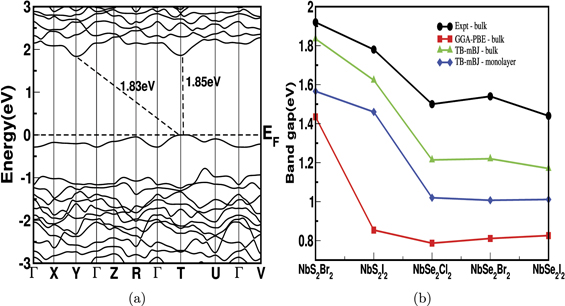
Figure 3. (a) The electronic band structure plotted against high symmetry points in BZ as shown in figure 1(b). The dotted line display the direct bandgap and indirect bandgap values. (b) Comparison of bulk and monolayer bandgap values (experimental band gap values are taken from reference [22].
Download figure:
Standard image High-resolution image
Figure 4. (a) The total and partial DOS for bulk structure of NbS2Br2 and (b) total DOS for NbX2Y2 (X = S, Se and Y = Cl, Br, I).
Download figure:
Standard image High-resolution image3.4. Transport properties
We now discuss the calculated transport properties for bulk NbX2Y2 based on the semi-classical Boltzmann transport theory. Thermoelectric properties of the investigated compounds are being calculated as a function of carrier concentration. Our results show that these compounds have large thermopower along with appreciable electrical conductivity, which is essential for a thermoelectric material. Also, all the compounds exhibit anisotropic nature in thermoelectric properties, which can be attributed to the low symmetry of triclinic systems. So, it is very important to analyse the properties in all the three crystallographic axes. The values of the band gaps are in the optimal range for a good thermoelectric performance. From the DOS plots, we can observe that all the five compounds have large DOS just below Fermi level, which is also reflected in the more flat nature of valence band in electronic band structure. Such an observed trend in the DOS is expected to result in larger thermopower [50].
Here, we have discussed the transport properties for the fixed optimal doping concentraion of 1019 cm−3 at room temperature T = 300 K. The calculated values of thermoelectric coefficients are shown in table 3. All the investigated compounds exhibit quite a large thermopower for both the carriers. For example, NbS2Br2 has thermopower value of around 484 μV K−1 for holes and NbSe2Cl2 has thermopower value of around 490 μV K−1 for electrons. The thermopower is decreasing as a function of carrier concentration and the same is increasing with temperature.
Table 3. The calculated thermopower S (in units μV K−1), electrical conductivity scaled by relaxation time σ/τ(in units Ω−1 m−1 s−1 and power factor S2 σ/τ (in units W mK−2 s−1) of NbX2Y2 for carrier concentration 1019 cm−3 at 300 K('a, b, c' are crystallographic axes).
| p-type | n-type | ||||||
|---|---|---|---|---|---|---|---|
| a | b | c | a | b | c | ||
| NbS2Br2 | S | 466.83 | 516.457 | 483.89 | 424.16 | 428.01 | 404.90 |
| (σ/τ) × 1017 | 0.44 | 0.50 | 1.26 | 3.09 | 1.49 | 0.11 | |
| (S2 σ/τ) × 1011 | 0.10 | 0.13 | 0.30 | 0.54 | 0.26 | 0.017 | |
| NbS2I2 | S | 441.07 | 464.88 | 470.65 | 405.01 | 403.62 | 346.37 |
| (σ/τ) × 1017 | 0.70 | 1.12 | 1.36 | 3.24 | 2.06 | 0.08 | |
| (S2 σ/τ) × 1011 | 0.14 | 0.25 | 0.30 | 0.53 | 0.33 | 0.009 | |
| NbSe2Cl2 | S | 448.69 | 478.18 | 454.90 | 467.08 | 434.87 | 490.19 |
| (σ/τ) × 1017 | 0.62 | 0.70 | 1.52 | 3.41 | 0.41 | 0.68 | |
| S2(σ/τ) × 1011 | 0.12 | 0.16 | 0.31 | 0.77 | 0.08 | 0.16 | |
| NbSe2Br2 | S | 426.36 | 459.45 | 424.96 | 419.01 | 421.46 | 457.70 |
| (σ/τ) × 1017 | 0.88 | 0.67 | 1.90 | 3.69 | 0.95 | 0.55 | |
| (S2 σ/τ) × 1011 | 0.17 | 0.14 | 0.34 | 0.64 | 0.16 | 0.12 | |
| NbSe2I2 | S | 424.46 | 431.78 | 426.19 | 397.30 | 402.60 | 394.92 |
| (σ/τ) × 1017 | 1.00 | 1.02 | 2.06 | 4.17 | 1.48 | 0.39 | |
| (S2 σ/τ) × 1011 | 0.17 | 0.19 | 0.37 | 0.65 | 0.24 | 0.06 | |
We have plotted the electrical conductivity scaled by relaxation time (σ/τ), due to the assumption of CSTA. The conductivity increases with the carrier concentration. The maximum electrical conductivity is observed along 'c' axis for holes and for the electrons along the 'a' axis. For instance, in NbSe2I2, the hole conductivity is 2.06 × 10¹⁷ Ω−1 m−1 s−1 along 'c' axis and the electron conductivity is 4.17 × 10¹⁷ Ω−1 m−1 s−1 along 'a' axis. In general, the electrical conductivity due to electrons is higher than that of holes, which is due to the more dispersive nature of the conduction band. The anisotropy of thermoelectric behaviour is an important highlight for the present series. Though the anisotropic nature of thermopower is less prominent along different directions, the anisotropy in electrical conductivity (σ/τ) is quite large which is reflected in the power factor (S2 σ/τ) as well. Also, the anisotropy in conductivity is more prominent for electrons compared to holes. The electrical conductivity of NbS2I2 for different directions and the ratio of electrical conductivity along different axes for NbS2I2 is shown in figures 5(a) and (b), from which we can observe that σa is 40 times higher than σc and σb is 25 times higher than σc which is huge anisotropy compared to earlier reports [51].

Figure 5. (a) Electrical conductivity for different directions and (b) ratio of calculated electrical conductivity of NbS2I2 at 300 K.
Download figure:
Standard image High-resolution imageThe calculated power factor for bulk NbX2Y2 is shown in figure 6 and 7. In general, the powerfactor is high for electrons compared to holes along 'a' and 'b' axes. But, we observed an opposite trend along 'c' axis where the power factor is high for hole carriers than electrons. For example in NbS2Br2, the S2 σ/τ for electrons along 'a' and 'b' axes are 0.54 × 10¹¹ (W mK−2 s−1) and 0.26 × 10¹¹ (W mK−2 s−1) respectively. But, for holes, along the same corresponding axes, it is 0.10 × 10¹¹ (W mK−2 s−1) and 0.13 × 10¹¹ (W mK−2 s−1). On the otherhand, the S2 σ/τ along 'c' axis is 0.30 × 10¹¹ (W mK−2 s−1) for holes and 0.017 × 10¹¹ (W mK−2 s−1) for electrons. Also, the maximum power factor of 0.77 × 10¹¹ (W mK−2 s−1) is observed in NbSe2Cl2, along 'a' axis for electron concentration. These results suggest that n-type carriers have better thermoelectric performance in 'a' axis for NbX2Y2. Also the average power factor for n-type is high compared to p-type. Therefore, comparing the behaviour of both electron and holes, we can conclude that the our compounds are more favourable for n-type doping.

Figure 6. The power factor scaled by relaxation time for bulk NbS2Br2 in (a) and (b) and NbS2I2 in (c) and (d).
Download figure:
Standard image High-resolution image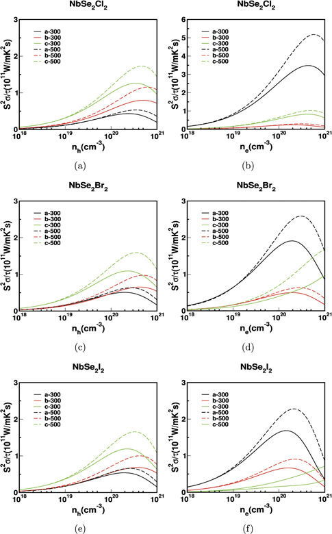
Figure 7. The power factor scaled by relaxation time for bulk NbSe2Cl2 in (a) and (b), NbSe2Br2 in (c) and (d) and NbSe2I2 in (e) and (f).
Download figure:
Standard image High-resolution imageFor a better thermoelectric performance, the material should have low lattice thermal conductivity. As mentioned earlier, the lattice thermal conductivity of NbX2Y2 is expected to be very low since they possess very low Debye temperature. Materials with low Debye temperature have more modes activated at room temperature. This causes high scattering rate of phonons due to the increasing phonon population. Moreover, the strong coupling between the acoustic branches and low lying optical branches can also induce more phonon scattering, thereby reducing the lattice thermal conductivity [52]. In order to estimate the lattice thermal conductivity of investigated compounds, we used Slack's model, which captures the experimental results more correctly [53]. The predicted values of lattice thermal conductivity and Gruneisen parameter of investigated compounds are shown in table 4. In particular, the κl of NbS2I2 is nearly 0.688 Wm−1 K−1. We observed that the calculated lattice thermal conductivity is very low [43, 54, 55]. Such a low thermal conductivity is desirable for any thermoelectric applications. Since the investigated compounds have high power factor and expected to have low lattice thermal conductivity, these compounds could be good candidates for future thermoelectric applications.
Table 4. The calculated lattice thermal conductivity (kl) and Gruneisen parameters of the investigated compounds of NbX2Y2 (X = S, Se and Y = Cl, Br, I) at 300 K.
| NbS2Br2 | NbS2I2 | NbSe2Cl2 | NbSe2Br2 | NbSe2I2 | |
|---|---|---|---|---|---|
| kl (in units W m−1 K−1) | 1.194 | 0.688 | 1.532 | 1.001 | 0.845 |
| Gruneisen parameter | 1.672 | 1.763 | 1.596 | 1.720 | 1.677 |
3.5. Optical properties
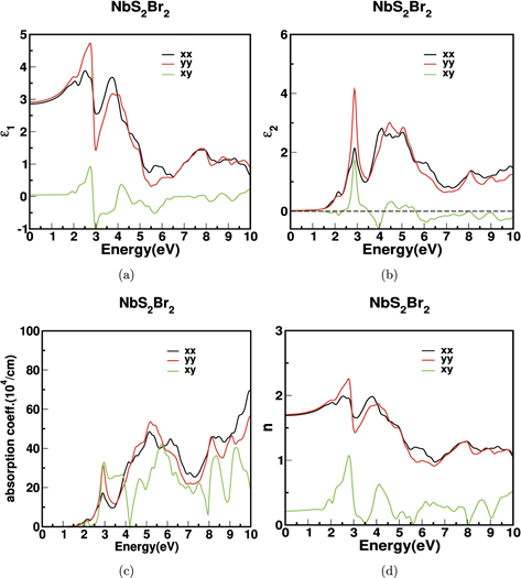
The optical properties of the NbX2Y2 compounds is studied for the energy range of 0–10 eV. The calculated real and the imaginary part of dielectric constants, refractive index, and absorption coefficient of NbS2Br2 are given in figure 8. The complex dielectric function is (ω) = 1(ω) + i2(ω), where 1 is the real part and 2 is the imaginary part of the dielectric function. Since it provides intrinsic optical characteristics of materials, the real and imaginary parts of the dielectric function spectra are known as 'optical constants'. Also, if we know imaginary part of the dielectric function, we can find real part of the dielectric function using Kramers–Kronig relation and the other optical properties, i.e., the refractive index n(ω) and absorption coefficient α(ω) etc, can be obtained from 1(ω) and 2(ω) [56].
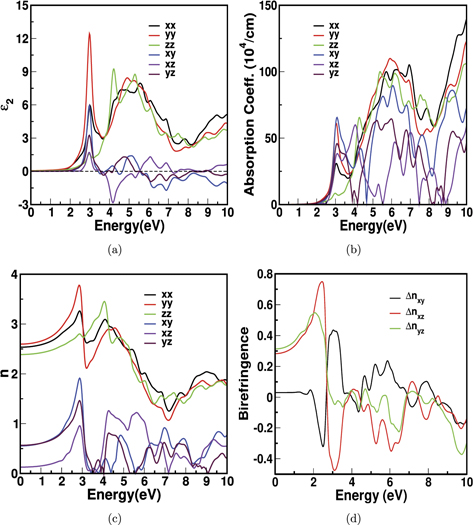
Figure 8. The optical properties for bulk structure of NbS2Br2, (a) the imaginary part of dielectric constant, (b) the absorption coefficient and (c) the refractive index, and the birefringence for NbSe2I2 in (d).
Download figure:
Standard image High-resolution imageThe dielectric tensor constants are position and symmetry dependent. According to the crystal symmetry, the dielectric tensor of triclinic structure is given as six independent components including off-diagonal elements and three frequency dependent parameters due to orientation of axes given as [14, 57, 58],

The static dielectric constant is an important factor used to estimate the capacitance based on the capacitance formula where, the static dielectric constant is directly proportionate to capacitance [59]. The static dielectric constants 1 are calculated from real dielectric part. The static dielectric part 1 is directly related with static refractive index n and is given by  . We have observed a strong anisotropy in static dielectric constant between cross plane direction z' and the in-plane directions 'x' and 'y'. The same trend is reflected in the calculated refractive indices, and the same are given in table 5.The maximum imaginary dielectric (2) response of the material in all the triclinic structures are in y-direction. The interband transition is mainly from the Nb-d states of valence band to the X-p or Y-p states of conduction band. Also, the first transition is observed in visible region and second transition is observed in ultra-violet (UV) region.
Table 5. Calculated anisotropy of the static refractive index for investigated compounds NbX2Y2 (X = S, Se and Y = Cl, Br, I).
| NbS2Br2 | NbS2I2 | NbSe2Cl2 | NbSe2Br2 | NbSe2I2 | |
|---|---|---|---|---|---|
| nx | 2.53 | 2.74 | 2.68 | 2.76 | 2.94 |
| ny | 2.59 | 2.71 | 2.72 | 2.79 | 2.91 |
| nz | 2.38 | 2.51 | 2.49 | 2.53 | 2.62 |
The optical absorption is an important factor of the material, considering any optoelectronic applications. The first peak is observed nearly at 2.5–3 eV in the visible region and as energy increases, we can observe the second peak at 5–6 eV in the UV region. The peak emerged from the electronic transition of Nb-d states in valence band to X-p and Y-p in conduction band. There are very few studies which reported the off-diagonal elements in the literature. For example, in Ga2O3, xz
= 0.3 and in CdWO4, 2xy
≈ 2 [15, 16]. But, in all of NbX2Y2, the off-diagonal components have high values. For instance, in NbS2Br2, the  . These huge off-diagonal values reflect in the anisotropy of other properties such as absorption coefficients and refractive indices.
The refractive index of the NbX2Y2 is given in table 5. The maximum refractive index observed in NbSe2I2 is 3.85 at 2.5 eV in the y-direction and the same is shown in supplementary figure 3. Clearly, the anisotropic nature is observed in the refractive index which can be measured from birefringence [60]. In general, a light ray entering a birefringent crystal splits into two propagating eigenstates with orthogonal linear polarization and different propagation directions. Each of the two polarization states experience a different refractive index. The static value of birefringence is calculated by Δnxy (nxx − nyy ), Δnxz (nxx − nzz ) and Δnyz (nyy − nzz ) and the same is shown in figure 8(d) for NbSe2I2 and the birefringence values for all the investigated compounds are given in table 6. The value of Δnxy is less than Δnxz and Δnyz . We have observed the maximum value of static birefringence to be 0.313 for NbSe2I2. Also the calculated value is much large compared to some reported common birefringent crystals such as CaCO3 (0.16) [61], YVO4 (0.26) [62], LiGaSe2 (0.045) [63] etc [64]. These interesting optical properties of NbX2Y2 compounds may certainly fetch possible applications in polarized devices, beam splitter [19] and scintillators [65].
Table 6. The calculated birefringence for bulk NbX2Y2.
| NbS2Br2 | NbS2I2 | NbSe2Cl2 | NbSe2Br2 | NbSe2I2 | |
|---|---|---|---|---|---|
| Δnxy | 0.061 | 0.023 | 0.070 | 0.025 | 0.030 |
| Δnxz | 0.148 | 0.246 | 0.192 | 0.234 | 0.313 |
| Δnyz | 0.208 | 0.223 | 0.233 | 0.260 | 0.282 |
4. Monolayer study
All the investigated compounds are layered and the layers are bound by weak van der Waal's interaction between inter layer atoms. The structure of NbS2Br2 monolayer is shown in figure 1(b). The dynamical stability of cleaved structures is confirmed through positive phonon modes in phonon dispersion and the same for NbS2Br2 is shown in figure 9(a). The low frequency optical modes are highly interacting with acoustic modes. The calculated bandstructure for NbS2Br2 is shown in figure 9(b) and we found that their band gap values are in the range of semiconductor which is given in figure 3(b). Usually, when we move from bulk to monolayer, the band gap value of monolayer is increased compared to bulk due to the quantum confinement effect. But, in the case of NbX2Y2, the band gap values of monolayers are found to be lower than their corresponding bulk values which indicates the anomalous quantum confinement effect (AQCE). The observed AQCE could be suitable for opto-electronic applications as reported earlier [66].
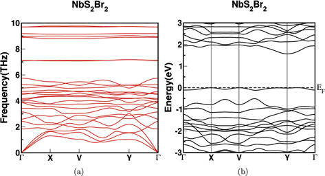
Figure 9. The electronic structure (a) and the phonon dispersion (b) of monolayer NbS2Br2 along high symmetry path in 2D plane as shown in figure 1(b).
Download figure:
Standard image High-resolution imageExperimental studies have demonstrated that the thermoelectric properties of different materials can be improved by dimension reduction of bulk to monolayer [67, 68]. The calculated power factor for monolayer NbX2Y2 is shown in figures 10 and 11. We have calculated thermoelectric properties of monolayer NbX2Y2 along the 'a' and 'b' axes. We have observed enhanced electrical conductivity in monolayer than bulk because of the reduced band gap of monolayer compared to that of bulk. The electrical conductivity for electrons is higher than for holes. The maximum electrical conductivity observed in 'b' axis for hole carriers and 'a' axis for electrons and the same thing reflects in the power factor. Just like their bulk counterparts, we have observed huge anisotropy in the electrical conductivity of monolayers as well. Also, we can observe the same anisotropy trend in power factor too.
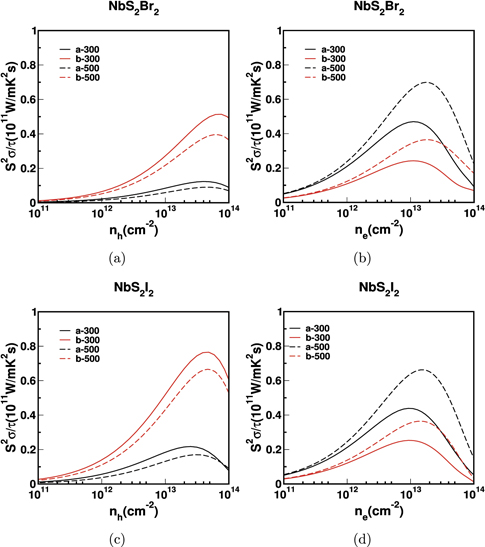
Figure 10. The power factor scaled by relaxation time for monolayer NbS2Br2 in (a) and (b) and NbS2I2 in (c) and (d).
Download figure:
Standard image High-resolution image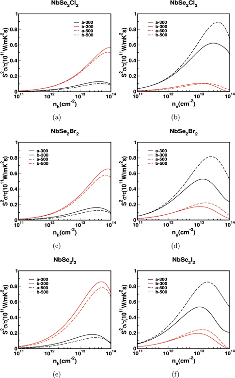
Figure 11. The power factor scaled by relaxation time for monolayer NbSe2Cl2 in (a) and (b), NbSe2Br2 in (c) and (d) and NbSe2I2 in (e) and (f).
Download figure:
Standard image High-resolution imageThe thermopower decreases when we move from S to Se and Cl to I. Also, in general, the thermopower for hole carriers are higher than electron carriers in both the bulk and monolayer. Substantial high Seebeck coefficient with value of around 200 μV K−1 can be found in both p-type and n-type cases up to nearly 1013 cm−2 [51]. The maximum Seebeck coefficient observed is along 'b' axis for p-type doping and along 'a' axis for n-type doping.
We have also calculated the optical properties for monolayer. The optical properties for NbS2Br2 monolayer are shown in figure 12. The static dielectric constant, which shows less anisotropy in 'x' and 'y' directions for the bulk, has become almost isotropic for the 2D monolayer system. Also the imaginary part of dielectric constant is consistent with the band gap of the monolayer. The maximum peak value of 2 is 12–14 for the bulk, whereas for the monolayer, it is reduced significantly with the value around 4–5 due to lesser screening effect in 2D systems [69]. We have observed the maximum peak for all elements of 2 tensor only around the visible region. Also, the transparent regions of bulk is more than monolayer because of the anomalous quantum confinement of band gap. The first peak of the absorption coefficient is observed at 3 eV to be about 6 × 105 cm−1 and the second peak at 5.8 eV to be at 12 × 105 cm−1. But, in the case of monolayer, the peaks are observed at 3 eV and 5.2 eV about 3 × 105 cm−1 and 6 × 105 cm−1 respectively. The value of refractive index of monolayer is around 2–2.5 which is comparable to the well known 2D materials like graphene (2.71) [70, 71], SnO (1.3) [72] etc. Moreover, the refractive index of off-diagonal elements is observed around nxy
≈ 1. It is to be noted that the refractive indices are isotropic in the low energy regime and there is no birefringence observed for the monolayer. The thermoelectric and optical properties of monolayer NbX2Y2 reveals that their layers are good candidate for exploring future low dimensional device applications [59].
Figure 12. The optical properties for monolayer of NbS2Br2, (a) real part of dielectric constant, (b) the imaginary part of dielectric constant, (c) the absorption coefficient and (d) the refractive index.
Download figure:
Standard image High-resolution image
5. Conclusion
The structural, mechanical, dynamical, thermoelectric and optical properties of NbX2Y2 (X = S, Se and Y = Cl, Br, I) are calculated within the framework of first principle study. The investigated compounds are mechanically and dynamically stable. The low frequency optical modes are highly interacting with the acoustic modes. The electronic structure properties reveal the semiconducting nature of these compounds. The thermoelectric properties of the investigated compounds infer the heavy doping applications with anisotropic nature. Soft phonon modes with very low Debye temperatures of these compounds indicates that they may have low lattice thermal conductivity, which is crucial for good thermoelectric performance. The optical properties reveals huge birefringence in all the compounds. The monolayer NbX2Y2 is also a semiconductor similar to bulk. The phonon dispersion of monolayer confirms its dynamical stability. In particular, the NbSe2I2 has promising thermoelectric performance as well as huge birefringence of 0.313 in mid-IR range, which make it a more interesting candidate for further experimental investigations. The good thermoelectric and optical properties observed in bulk and layered semiconducting compounds make them suitable for many optical-electronic applications such as light emitting devices (LED), memory devices, scintillators, photovoltaic and thermoelectric devices. The giant birefringence observed might fetch attention for non-linear optical applications.
Acknowledgments
The authors ARN, PK, VKS and VK would like to thank IIT Hyderabad for computational facility. ARN would like to thank CSIR for fellowship. PK and VK would like to acknowledge to BRNS project with Sanction No. (58/14/13/2019-BRNS).
GV acknowledges, CMSD, University of Hyderabad for providing computational facility.
Data availability statement
The data generated and/or analysed during the current study are not publicly available for legal/ethical reasons but are available from the corresponding author on reasonable request.