

Abstract
The efficiency and bandwidth of an optical absorbing material, especially for the promising two-dimensional transition metal dichalcogenides (TMDCs) are critical to underpin advances in photonic and optoelectronic devices. In this work, we present a general method to manipulate the bandwidth of an absorber with high efficiency through coupling with the quasi-bound states in the continuum (quasi-BIC). We demonstrate this strategy by taking absorbing material monolayer TMDC coupled with the lossless symmetry-broken photonic crystal (PhC) slab. An optimal-efficiency TMDC-based absorber with over three orders of magnitude of bandwidth adjustment is realized, by simultaneously adjusting the structure asymmetry parameter of PhC slab and the locations of monolayer TMDC in the structure. Interestingly, the absorption bandwidth is tailored quadratically with the asymmetry parameter, which derived from the powerful physics of bound state in the continuum (BIC) in radiation engineering. Moreover, a superior-performance optical refractive index sensor is further designed. We demonstrate that our proposed method based on quasi-BIC structure can also effectively govern the sensing performance. Present work not only provides further insight into BIC physics, but also offers a promising strategy of smart engineering in active optical devices with the properties on demand.
Export citation and abstract BibTeX RIS
1. Introduction
Atomically thin two-dimensional (2D) transition-metal dichalcogenides (TMDCs) such as MoS2, WSe2, WS2, and MoSe2 have recently attracted intensive attention in photonic and optoelectronic applications because of their semiconducting nature and distinctive optical properties [1–3]. One of the most appealing potentials of TMDCs is to enable new functionalities beyond the capabilities of conventional bulk materials. A major challenge of these TMDCs materials to hindering the device development is relatively low light absorption stemming from the inherent atomic thickness. For instance, the light absorption of monolayer MoS2 or WS2 is about 5%–10 in the visible spectrum [4, 5]. To solve this issue, the hybrid configuration via combining monolayer TMDCs with a resonant structure was proposed, whose underlying physical mechanism can be attributed to critical coupling [6, 7]. It is found that the maximum and even perfect absorption could be approached when absorption rate of monolayer TMDC equals radiation rate of the resonant structure. Rooted in this thinking, various resonant structures, such as photonic crystal (PhC) slab [5, 8–10], metamaterials and metasurfaces [11–14], or plasmonic structure [15–19], were designed and utilized. However, most works focused on the detailed structure parameters to optimize absorption efficiency, while paid little attention to absorption bandwidth. To explore a simple and general way to simultaneously realize the high-efficiency absorption and manipulate the absorption bandwidth for TMDCs is certainly important.
With the strategy of critical coupling, the radiation engineering of the resonant structure plays a vital role in tailoring light absorption performance. The resonant structure with high radiation capability over a wide range is needed. Recently, the developed concept of bound states in the continuum (BICs) in nanophotonics offered a simple way to engineer radiation behavior for various all-dielectric structures [20–23]. A BIC is eigenmode which holds an infinite lifetime and could not radiate out, even in a structure with open channels to free space. When in-plane inversion symmetry of structure is broken, it could be transformed into a quasi-bound states in the continuum (quasi-BIC) with finite lifetime and has radiation capability [24]. This functionality is highly desirable and would be particularly favorable for the manipulation of light absorption performance especially for TMDCs.
In this letter, we demonstrate a strategy by coupling with a symmetry-broken quasi-BIC excited in a PhC slab, to effectively manipulate the absorption performance, i.e. efficiency and bandwidth, of monolayer TMDCs. Based on the temporal coupled-mode theory (CMT) [25–27], we derive how two key parameters, radiation rate γr and absorption rate γa of an optical resonator, determine its absorption performance. It shows that to tailor absorption performance, it needs to adjust γr and γa simultaneously over a wide range. Interestingly, it is found that γr of symmetry-broken quasi-BIC can be adjusted significantly by the structure asymmetry parameter. γa of monolayer TMDCs can be readily controlled by changing its location in the resonance structure. Based on this, the absorption bandwidth of monolayer TMDCs can be adjusted than three orders of magnitude meanwhile maintaining its absorption efficiency at a maximum value. An ultra-narrow-band and even infinitely narrow-band absorber can be realized. Moreover, thanks to the property that γr of quasi-BIC resonance could be adjusted to an ultra-low value, an optical refractive index (RI) sensor with superior performance is realized. Its sensitivity and especially figure-of-merit (FOM) can be adjusted effectively. This work shows the mighty radiation engineering capability of quasi-BIC resonance and would provide further step in 2D material optical devices such as harvesting, light emitting devices, sensor and modulators.
2. Theoretical analysis
We employ the CMT to derive the optimal absorption conditions of the optical resonator. Figure 1(a) shows the theoretical model, which consists of a single-mode optical resonator with amplitude a coupled with two ports. Its optical behavior can be described by a CMT equation: [25–27]

where ω0 is the resonant frequency, γr
is the radiation coupling rate of the resonance mode to the outgoing wave, and γa
is the intrinsic dissipative rate mainly originating from material absorption, respectively. The vectors  and
and  are the amplitude of the flux of incoming and outgoing plane waves.
  represents the coupling coefficient between the resonance and the ports. The scattering matrix C describes the direct pathway between incoming and outgoing waves in the absence of the resonance mode.
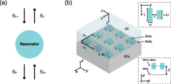
Figure 1. (a) Schematic view of a single optical resonator coupled to two free-space ports. The arrows indicate the incoming and outgoing waves of each port. (b) Schematic view of the proposed high-performance TMDC-based absorber with adjustable absorption bandwidth through coupling with the quasi-BIC resonance structure. The quasi-BIC structure is constructed by the lossless PhC slab with broken in-plane inversion symmetry.
Download figure:
Standard image High-resolution imageThe resonance mode can be written as  . Substituting into equation (1), we can obtain
Due to energy conservation and reciprocal theorem, one can show that  and
and  . Therefore
  and
and  . We further consider the resonator with mirror symmetry. It implies the resonance mode coupled to each port with the same rate,
  . Then under excitation from a single port, for example
  , the light absorption of the optical resonator can be derived as
It can be seen that the absorption formula exhibits a symmetric Lorentzian lineshape. The absorption peak of value A0 occurs at the resonant frequency ω0,
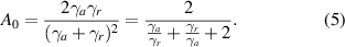
The absorption peak A0 is mainly determined by the ratio between radiation rate γr
and absorption rate γa
. When  , namely critical coupling [28], the absorption for a single-mode two-port optical resonator reaches its maximum
  .
.
Moreover, the absorption bandwidth can be obtained. The absorption bandwidth  is defined as the full width at half maximum (FWHM). Suppose the half maximum absorption A1 occurs at the frequency ω1, it has
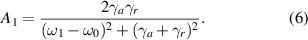
From  and
and  , the absorption bandwidth can be easily obtained as

This reveals that the principle to design a high-efficiency absorber with adjustable absorption bandwidth is to simultaneously adjust γr
and γa
at critical coupling. At critical coupling condition,  . We can find that the radiation capability of the resonant structure directly affects the performance of the light absorption bandwidth. Therefore, γr
should be engineered as widely as possible.
. We can find that the radiation capability of the resonant structure directly affects the performance of the light absorption bandwidth. Therefore, γr
should be engineered as widely as possible.
To fully engineer radiation γr
, we consider the photonic structure with broken in-plane inversion symmetry supporting BIC-inspired Fano resonance, i.e. quasi-BIC (see figure 1(b)). The original structure holding the in-plane symmetry (x–y plane) supports the symmetry-protected BIC with  , without radiation ports to the free space. As the structure asymmetry parameter evolves, the radiation ports are opened and
  . γr
can be calculated analytically as a sum of radiations into all ports [24]
. γr
can be calculated analytically as a sum of radiations into all ports [24]
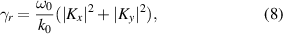
here k0 is the wave vector, and  are the quasi-BIC coupling amplitudes in the ports of two orthogonal polarizations.
  can be expressed as
where S0 is the surface area of a unit lattice, p, m and Q represent the components of electric dipole, magnetic dipole and electric quadrupole moments per unit lattice, respectively [29, 30]. For BIC, the electric field Ex
and Ey
are always odd due to the symmetry conservation with respect to (x,y) (−x,−y) transformation, so
  and γr
are zero. If breaking the in-plane symmetry in the y axis, i.e. breaking the inversion of coordinates (x,y)
and γr
are zero. If breaking the in-plane symmetry in the y axis, i.e. breaking the inversion of coordinates (x,y) (−x,−y), Kx
exists since Ex
will become even function. And thanks to the up-down mirror symmetry, both my
and
(−x,−y), Kx
exists since Ex
will become even function. And thanks to the up-down mirror symmetry, both my
and  are zero. Therefore, equation (8) can be simplified as
For quasi-BIC, the net dipole moment px
can be rewritten by  , where p0 corresponds to the dipole moment of symmetric case and δ is the structure asymmetry parameter. Then we can get

where γ0 is a constant independent of δ. We can also obtain the absorption bandwidth  at critical coupling condition,

It shows that  at critical coupling and γr
exhibit the quadratic dependence on δ. Thus, using quasi-BIC structure is one realistic way to precisely manipulate the absorption bandwidth of an optical absorber with high efficiency.
at critical coupling and γr
exhibit the quadratic dependence on δ. Thus, using quasi-BIC structure is one realistic way to precisely manipulate the absorption bandwidth of an optical absorber with high efficiency.
3. Absorption performance
To construct quasi-BIC structure, here we employ the lossless PhC slab. As shown in figure 1(b), the unit lattice composes of a pair of parallel and geometrically asymmetric Si3N4-bars deposited atop a glass substrate. To keep its out-of-plane mirror symmetry, the PhC slab is immersed in the index-matched oil environment. The introduced length perturbation  for one of a pair of bars in the x direction is used to break in-plane inversion symmetry. The asymmetry parameter δ is characterized by
  . The simulations are performed by 2D rigorous coupled-wave analysis (Diffract MODE, RSOFT), a commercially available software [31, 32]. In the simulations, the refractive indices of Si3N4 and SiO2 are set as 2.02 and 1.46, respectively. The periodicity of PhC slab along the x- and y-axis are
  nm and
  nm, respectively. The thickness h and width w of each bar, and the separation distance s between two bars are fixed as h = 180 nm, w = 85 nm, and s = 80 nm, respectively. For symmetric case δ = 0, the bar length is L = 270 nm. The incident light source is along the −z direction with linear electric polarization parallel to the x direction.
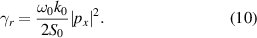
To confirm the existence of a quasi-BIC in our proposed PhC slab, we first perform numerical analysis of its optical spectra. The transmission spectra as a function of incidence angle θ for the symmetric (upper) and asymmetric (lower) PhC slab are compared in figure 2(a). For the symmetric case (upper), the resonance disappears at-Γ point, confirming the existence of symmetric-protected BIC at-Γ point [22]. For the asymmetric case (lower), the trend of the transmission spectra with θ is highly consistent with the symmetric case (upper), except that it is not BIC at-Γ point. That means that, by breaking the in-plane inversion symmetry, the resonance mode at-Γ point changes from a BIC state without radiation capability to a leaky mode, i.e. quasi-BIC [24]. Figure 2(b) further demonstrates the similarity of the electric fields between BIC and quasi-BIC. The transmission spectra at normal incidence as a function of wavelength and δ are shown in figures 2(c) and (d). It is found that the quasi-BIC behavior is closely related to δ. The transmission spectra of quasi-BIC for asymmetric structure δ ≠ 0 exhibits a Fano resonance that will vanish for symmetric structure δ = 0. More importantly, the bandwidth of transmission spectra for quasi-BIC continuously increases with δ. It indicates a positive correlation between γr of quasi-BIC and δ.
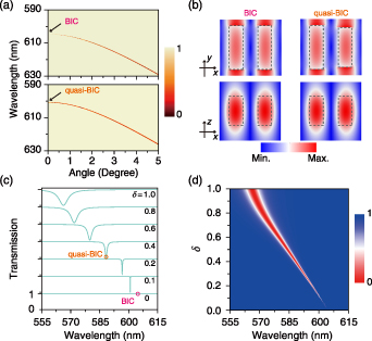
Figure 2. (a) Transmission spectra as a function of incidence angle θ and wavelength for the symmetric (upper) and asymmetric (lower) PhC slab. The structure asymmetry parameter δ of the asymmetric (lower) PhC slab is 0.1. (b) The electric-field distributions in the area of unit lattice for both BIC (left) and Quasi-BIC (right). The black dashed lines indicate Si3N4 bars. (c) and (d) Evolution of the transmission spectra at normal incidence as a function of wavelength and δ.
Download figure:
Standard image High-resolution imageThe values of γr
can be obtained by fitting transmission spectra near a guided resonance within the CMT framework [20]. Figure 3(a) presents the transmission spectrum of the asymmetric PhC slab for δ = 0.3 and  . It shows that the theory agrees excellently with the simulation result. Figure 3(b) summarizes γr
of the quasi-BIC resonance with different δ, which shows a quadratic dependence of γr
on δ. It verifies the results of the theoretical derivation in equation (11). It can be seen that as δ taking value from 0 to 1, γr
increases from zero and changes by well over three orders of magnitude. This is very beneficial for achieving a high-performance absorber with a wide range of adjustable bandwidth.
. It shows that the theory agrees excellently with the simulation result. Figure 3(b) summarizes γr
of the quasi-BIC resonance with different δ, which shows a quadratic dependence of γr
on δ. It verifies the results of the theoretical derivation in equation (11). It can be seen that as δ taking value from 0 to 1, γr
increases from zero and changes by well over three orders of magnitude. This is very beneficial for achieving a high-performance absorber with a wide range of adjustable bandwidth.
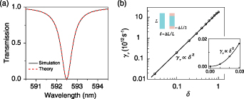
Figure 3. (a) Simulated (black curve) and fitted (red dashed curve) transmission spectra of of the asymmetric PhC slab with δ = 0.3. (b) Radiation rate γr of the quasi-BIC resonance as a function of the structure asymmetry parameter δ. To show clearly, the different coordinate scales are used for graphing. The black curves represent the fitted results with the quadratic dependence.
Download figure:
Standard image High-resolution imageAccording to the theory presented above, to tailor absorption bandwidth of an absorber with high efficiency, it needs to simultaneously adjust γr
and γa
at critical coupling. γr
can be adjusted using the quasi-BIC supported by the PhC slab that depends on the structure asymmetric parameter δ. Thus, γa
of the absorbing material needs to be adjusted to match γr
of the quasi-BIC structure. γa
is directly related to the amount of absorbing material, i.e. its intrinsic absorption coefficient. If the absorbing material we consider is fixed as monolayer MoS2, γa
seems unchangeable. Interestingly, we find that γa
of monolayer MoS2 is also closely related to the field distribution of the resonance mode and can be adjusted by changing its location in the resonance structure. Figure 4 shows the simulated absorption performance of monolayer MoS2 with its different locations in the PhC slab. The distance of monolayer MoS2 from the out-of-plane mirror plane of the PhC slab is denoted as d (see figure 1(b)). The thickness and permittivity of the monolayer MoS2 are adopted from experimental data [33]. From figure 4, on one hand, we can find that the absorption efficiency of bare monolayer MoS2 without the PhC slab is relatively low, only around 5 (red curve in figure 4(a)). By coupling with the PhC slab, the absorption efficiency of monolayer MoS2 can be remarkably increased even to
  , i.e. critical coupling. The critical coupling conditions (marked by the arrows in figure 4) for different d's can be readily found through changing the structure asymmetric parameter δ. On the other hand, it can be seen that the absorption bandwidth
  of monolayer MoS2 can be effectively adjusted, showing that the further away from the mirror plane of the PhC slab, the narrower the bandwidth is. Specifically, from figures 4(a) to (e), the critical coupling conditions occur at δ = 0.85 for d = 0 nm, δ = 0.45 for d = 110 nm, δ = 0.34 for d = 190 nm, δ = 0.234 for d = 290 nm, δ = 0.106 for d = 390 nm, and δ = 0.025 for d = 590 nm (inset in figure 4(e)), respectively. The corresponding rates can be extracted as
  , 3.9, 2.18, 1.02, 0.21, and 0.012
  s−1, respectively. Through simultaneously adjusting the structure asymmetry parameter δ of the PhC slab and the locations d of monolayer TMDC in the structure, the absorption bandwidth can be adjusted over three orders of magnitude from about 12 to 0.01 nm. In principle, we can continue to adjust the location of monolayer MoS2 to acquire the desired absorption bandwidth.
Figure 4. (a)–(e) Upper panels show absorption spectra of monolayer MoS2 as a function of wavelength and structure asymmetry parameter δ. Lower black curves correspond to monolayer MoS2 absorption at critical coupling condition for different locations in the PhC slab. Critical coupling conditions are marked by black arrows in upper panels. From (a) to (e), the distance d of monolayer MoS2 from the mirror plane of the PhC slab are d = 0, 110, 190, 290 and 390 nm, respectively. The corresponding critical coupling conditions occur at δ = 0.85, 0.45, 0.34, 0.234, and 0.106, respectively. The red curve in (a) shows the absorption of bare monolayer MoS2. Inset in (e): detailed absorption spectrum of monolayer MoS2 for d = 390 nm (left) and d = 590 nm (right) around resonant peak.
Download figure:
Standard image High-resolution imageFigure 5(a) summarizes the results shown in figure 4 and shows the critical coupling absorption of monolayer MoS2 with different d as a function of normalized resonance wavelength. It is clearly seen that  of monolayer MoS2 at critical coupling can be sufficiently tailored by changing its location d in the PhC slab. By fitting absorption spectra using equation (4), we can obtain γa
and γr
of the whole structure for different d. The results are shown in figure 5(b). The arrow shows the trend of increasing d. With increasing d, both rates are manipulated on the critical coupling condition
of monolayer MoS2 at critical coupling can be sufficiently tailored by changing its location d in the PhC slab. By fitting absorption spectra using equation (4), we can obtain γa
and γr
of the whole structure for different d. The results are shown in figure 5(b). The arrow shows the trend of increasing d. With increasing d, both rates are manipulated on the critical coupling condition  and the total damping rate
  is decreasing. And for the reason of decreasing of γa
with increasing d, it is closely related to the field distribution of the resonance mode. From figure 2(b), the field intensity decreases with increasing d, whose behavior is similar to that of γa
. It implies that the weaker the quasi-BIC field is, the less photons are absorbed by monolayer MoS2, naturally leading to decrease of γa
. Therefore, to realize critical coupling condition, γr
also needs to decrease to match γa
. That is why far away from the PhC slab, the critical coupling conditions occur at the lower δ (see the arrows positions in figure 4). It can be predicted that since γa
could approach zero when putting monolayer MoS2 at infinity where the field intensity is close to zero and γr
of quasi-BIC could also be adjusted down to zero,
is decreasing. And for the reason of decreasing of γa
with increasing d, it is closely related to the field distribution of the resonance mode. From figure 2(b), the field intensity decreases with increasing d, whose behavior is similar to that of γa
. It implies that the weaker the quasi-BIC field is, the less photons are absorbed by monolayer MoS2, naturally leading to decrease of γa
. Therefore, to realize critical coupling condition, γr
also needs to decrease to match γa
. That is why far away from the PhC slab, the critical coupling conditions occur at the lower δ (see the arrows positions in figure 4). It can be predicted that since γa
could approach zero when putting monolayer MoS2 at infinity where the field intensity is close to zero and γr
of quasi-BIC could also be adjusted down to zero,  can be infinitely narrow.
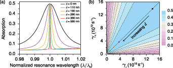
Figure 5. (a) Absorption of monolayer MoS2 with different locations d in the PhC slab versus normalized resonance wavelength. Black, purple, yellow, green, red and cyan curves represent the absorption of monolayer MoS2 with d = 0, 110, 190, 290, 390 and 590 nm, respectively. (b) Absorption efficiency contour as a function of radiation rate γr and absorption rate γa and the decay rates of monolayer MoS2 with different locations d in the PhC slab fitted from the spectra in figure 4 via the CMT. The color of the hollow dots corresponds to (a). The arrow shows the trend of increasing d. Parameters of the PhC slab are the same as those shown in figure 4.
Download figure:
Standard image High-resolution imageThe dependence of the absorption bandwidth  on the structure asymmetry parameter δ is further investigated.
  of monolayer MoS2 with different locations d in the PhC slab can be extracted from the absorption spectra in figure 4. As shown in figure 6, it can be found that
  is tailored quadratically on the asymmetry parameter δ, with a similar behavior to that of the radiation rate γr
. From equations (11) and (12), we can get
is tailored quadratically on the asymmetry parameter δ, with a similar behavior to that of the radiation rate γr
. From equations (11) and (12), we can get  .
.  is shifted with a value of
  relative to
  . Thus, the result in figure 6 is consistent with our theoretical derivation. It should be noted that the quadratic behavior of γr
on the asymmetry parameter δ originates from the general concept of BIC in the symmetry-broken Fano structure. This quadratic scalability is in principle not limited to a specific mode of a certain resonator, e.g. guided modes in the PhC slab presented in this work, but also is applicable to others such as trapped modes in the plasmonic and dielectric structures [34–36]. Meanwhile, the way of adjusting γa
by altering the locations of monolayer MoS2 in the resonant structure can be extended to other absorbing materials, such as graphene [37] and black phosphorus [38].
. Thus, the result in figure 6 is consistent with our theoretical derivation. It should be noted that the quadratic behavior of γr
on the asymmetry parameter δ originates from the general concept of BIC in the symmetry-broken Fano structure. This quadratic scalability is in principle not limited to a specific mode of a certain resonator, e.g. guided modes in the PhC slab presented in this work, but also is applicable to others such as trapped modes in the plasmonic and dielectric structures [34–36]. Meanwhile, the way of adjusting γa
by altering the locations of monolayer MoS2 in the resonant structure can be extended to other absorbing materials, such as graphene [37] and black phosphorus [38].
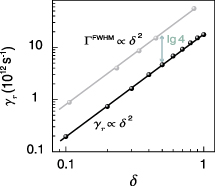
Figure 6. Quadratic dependence relationship of the absorption bandwidth  of monolayer MoS2-based absorber at critical coupling and γr
of the quasi-BIC resonance versus the structure asymmetry parameter δ.
of monolayer MoS2-based absorber at critical coupling and γr
of the quasi-BIC resonance versus the structure asymmetry parameter δ.
Download figure:
Standard image High-resolution imageWe can also adjust the quasi-BIC resonance to the wavelength range of monolayer MoS2 exciton. The absorption bandwidth at critical coupling can likewise be adjusted. The difference is critical coupling condition. The absorption of monolayer MoS2 exciton is higher. When coupling with the PhC slab, it has a higher γa . Achieving critical coupling requires higher γr (also corresponding to larger δ). The details are shown in the supplemental material [39] (is available online at stacks.iop.org/JPD/54/485106/mmedia). Moreover, our proposed structure like a toy model is also feasible in practice even though TMDCs are too fragile to be fabricated. The PhC slab can be fabricated successfully by electron-beam lithography and reactive ion etching, and the etching depth of the PhC slab can be precisely controlled by etching time. The locations of monolayer TMDCs in the PhC slab can be controlled by depositing spacer layer (such as silica) or spin-coating PMMA with certain thickness. The monolayer TMDCs can be transferred onto the PhC slab or embedded in dielectric films using the methods demonstrated in the [13, 40–42]. Therefore, the proposed method that manipulating absorption performance by controlling both rates shows general and viable property, possibly paving the way toward smart design in advanced photonic devices.
4. Sensing performance
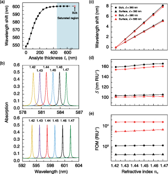
Below as an example of the application, a RI sensor based on the proposed quasi-BIC structure is presented. It shows that the RI sensor performance can also be adjusted effectively by our proposed quasi-BIC structure. The performance of a RI sensor is usually quantified by two parameters, sensitivity ( ) and FOM (
 ). It is well known that the lower
  of resonance mode helps to improve the detection limits of the RI sensor [43, 44]. With this consideration, we choose the narrow-band critical coupling system with the same parameters as shown in figure 4(e). The oil liquid originally covering the PhC slab is replaced with the analyte to be detected. Firstly, the RI nc
of the analyte is fixed as 1.46 and the dependence of peak wavelength on the analyte thickness tc
is investigated. As shown in figure 7(a), the peak wavelengths of RI sensor exhibit a redshift when increasing tc
from 0 nm (without analyte) to 450 nm. The corresponding wavelength shift can reach about 53 nm. When further increasing the analyte thickness tc
from 450 to 650 nm, the peak wavelength shift increases slowly into a saturated value (shown in the light blue shaded area) and even the peak wavelength is almost same as that of the bulk analyte with an infinite thickness (marked by red dot). This phenomenon is understandable. From figure 2(b), we can find that the electric field of quasi-BIC is intensively confined inside the PhC slab. When the analyte is relatively thin, comparable to the thickness of PhC slab, the near-filed interaction between the quasi-BIC field and analyte is quite strong, leading to a sharp increase of peak wavelength with the analyte thickness. When the analyte is thicker, part of the analyte is located in the fringing electric field and the analyte that can interact with the quasi-BIC field are limited, only in the area close to the PhC slab. This causes saturation of peak wavelength shift. These results indicate that our proposed RI sensor based on the quasi-BIC structure is extremely sensitive to the minor variation in the analyte thickness and could be applied in sensitive identification application for small volume of analyte. The structure presented here offers a promising opportunity in designing a high-performance absorber or RI sensor device.
of resonance mode helps to improve the detection limits of the RI sensor [43, 44]. With this consideration, we choose the narrow-band critical coupling system with the same parameters as shown in figure 4(e). The oil liquid originally covering the PhC slab is replaced with the analyte to be detected. Firstly, the RI nc
of the analyte is fixed as 1.46 and the dependence of peak wavelength on the analyte thickness tc
is investigated. As shown in figure 7(a), the peak wavelengths of RI sensor exhibit a redshift when increasing tc
from 0 nm (without analyte) to 450 nm. The corresponding wavelength shift can reach about 53 nm. When further increasing the analyte thickness tc
from 450 to 650 nm, the peak wavelength shift increases slowly into a saturated value (shown in the light blue shaded area) and even the peak wavelength is almost same as that of the bulk analyte with an infinite thickness (marked by red dot). This phenomenon is understandable. From figure 2(b), we can find that the electric field of quasi-BIC is intensively confined inside the PhC slab. When the analyte is relatively thin, comparable to the thickness of PhC slab, the near-filed interaction between the quasi-BIC field and analyte is quite strong, leading to a sharp increase of peak wavelength with the analyte thickness. When the analyte is thicker, part of the analyte is located in the fringing electric field and the analyte that can interact with the quasi-BIC field are limited, only in the area close to the PhC slab. This causes saturation of peak wavelength shift. These results indicate that our proposed RI sensor based on the quasi-BIC structure is extremely sensitive to the minor variation in the analyte thickness and could be applied in sensitive identification application for small volume of analyte. The structure presented here offers a promising opportunity in designing a high-performance absorber or RI sensor device.
Figure 7. The performance of a RI sensor based on quasi-BIC-governed monolayer MoS2-based absorber. (a) Dependence of peak wavelength on the analyte thickness tc . The RI nc of the analyte is 1.46 and the structure parameters of the RI sensor are the same as those shown in figure 4(e). In this case, the location of monolayer MoS2 is at d = 390 nm. The light blue shaded area represents saturated region. (b) Absorption spectra for surface analyte sensing (upper) and bulk analyte sensing (lower) as a function of RI nc of analyte. nc is varied from 1.42 to 1.47 in steps of 0.01. (c) Wavelength shift, (d) sensitivity and (e) FOM of RI sensor with monolayer MoS2 at two locations d = 390 nm (black dots) and 590 nm (red dots) for surface analyte sensing (triangle dots) and bulk analyte sensing (circle dots) as a function of nc . The dashed lines in (c) show the linear fittings.
Download figure:
Standard image High-resolution image
Next, we discuss specifically the performance of this RI sensor for two thicknesses of analyte. One is a finite thickness analyte, i.e. surface analyte, and the other is an infinite thickness analyte, i.e. bulk analyte. The thickness of surface analyte we choose is  nm. Figure 7(b) shows the absorption spectra for surface analyte sensing (upper) and bulk analyte sensing (lower) as a function of RI nc
of analyte. It can be seen that the peak wavelengths exhibit a substantial redshift despite the small increase in nc
. Figure 7(c) shows the extracted peak wavelengths as a function of nc
. For comparison sake, the wavelength shift is calculated as
nm. Figure 7(b) shows the absorption spectra for surface analyte sensing (upper) and bulk analyte sensing (lower) as a function of RI nc
of analyte. It can be seen that the peak wavelengths exhibit a substantial redshift despite the small increase in nc
. Figure 7(c) shows the extracted peak wavelengths as a function of nc
. For comparison sake, the wavelength shift is calculated as  , here
  corresponds to the resonance wavelength with the RI nc
of analyte and
corresponds to the resonance wavelength with the RI nc
of analyte and  corresponds to that of
  . A good linearity in fitting the shift of the resonance wavelength can be found (dashed line). Obviously, as nc
increases from 1.42 to 1.47, the wavelength shift for bulk analyte sensing can reach 8.2 nm (black circle dots), higher than surface analyte sensing with 5.2 nm wavelength shift (black triangle dots). The corresponding sensitivity for bulk analyte sensing is about
. A good linearity in fitting the shift of the resonance wavelength can be found (dashed line). Obviously, as nc
increases from 1.42 to 1.47, the wavelength shift for bulk analyte sensing can reach 8.2 nm (black circle dots), higher than surface analyte sensing with 5.2 nm wavelength shift (black triangle dots). The corresponding sensitivity for bulk analyte sensing is about  , higher than
  of surface analyte sensing, as shown in figure 7(d). We further calculate the FOM for both cases. From figure 7(b), we can find that the absorption peaks for both cases are always persisted at critical coupling with varying nc
from 1.42 to 1.47, leading to a nearly invariable
of surface analyte sensing, as shown in figure 7(d). We further calculate the FOM for both cases. From figure 7(b), we can find that the absorption peaks for both cases are always persisted at critical coupling with varying nc
from 1.42 to 1.47, leading to a nearly invariable  . This implies that the FOM for both cases does not vary with nc
. As shown in figure 7(e), the FOM for bulk analyte sensing (black circle dots) can reach 1165
. This implies that the FOM for both cases does not vary with nc
. As shown in figure 7(e), the FOM for bulk analyte sensing (black circle dots) can reach 1165  , which is about 2.8 times that of surface analyte sensing (black triangle dots).
It should be noted that the higher FOM can also be within reach by utilizing a narrower-band quasi-BIC resonance structure corresponding to a smaller asymmetry parameter δ. We can put monolayer MoS2 further away from the PhC slab, such as d = 590 nm. In this case, the condition for achieving the critical coupling of monolayer MoS2 is δ = 0.025. As shown in figure 7(c), the wavelength shift behavior as a function of nc
for monolayer MoS2 at d = 590 nm (red dots) is similar to that of monolayer MoS2 at d = 390 nm (black dots). The wavelength shift range of the former is slightly less than the latter. This result is related to the radiation capability of the quasi-BIC supported by the PhC slab. According to quadratic dependence relationship of γr
on δ, the quasi-BIC of the former has a lower γr
and is more difficult to couple with the environment, making it more insensitive to environment changes. Thus, the sensitivity of the former RI sensor is slightly lower than that of the latter. As shown in figure 7(d), the sensitivities of monolayer MoS2 at d = 590 nm for surface analyte sensing (red triangle dots) and bulk analyte sensing (red circle dots) are  and
and  , respectively. However, it is interesting that the FOM can be enhanced dramatically. As shown in figure 7(e), we can find that the FOM of monolayer MoS2 at d = 590 nm for surface analyte sensing (red triangle dots) can reach about 5800
  , 14 times more than that of monolayer MoS2 at d = 390 nm. And for bulk analyte sensing (red circle dots), the FOM also increases by over one order of magnitude, to 15 570
  .
.
Ultimately, a comparison of the sensing performance of state-of-the art bulk RI sensors is shown in table 1. We can find that our proposed structure has high sensitivity and especially ultrahigh FOM, indicating its superiority in sensing application. It should be noted that the sensitivity of plasmonic sensor is higher than our work. This is due to the natural advantages of metal surface plasmons, which have strong local field and are sensitive to the changes of dielectric medium. However, the FOM values of plasmonic sensors are generally low and difficult to dramatically enhance, due to the high intrinsic absorption of the metal material. The FOM is a more meaningful parameter to evaluate a RI sensor performance because it considers both the sensitivity and Q factors. A RI sensor with the high FOM (high Q factor) is desired in the detection of a small frequency shift induced by the little variation of dielectric medium or low volume of the analyte. In other words, the high FOM is desired in the detection of trace-amount substances. Therefore, with its high sensitivity and ultrahigh FOM, our proposed structure has prominent superiority and great potential for ultra-sensitive sensing applications.
Table 1. Comparison of the bulk RI sensing performance including structure type, working wavelength, sensitivity, and FOM of sensors.
| Reference | Structure type | Working wavelength | Sensitivity (nm ) ) | FOM ( ) ) |
|---|---|---|---|---|
| [19] | Plasmonic structure | Near IR | 119–249 | 15.9–22.6 |
| [16] | Plasmonic structure | Visible | 490–560 |
 21 21 |
| [45] | Plasmonic structure | Visible | 1006 | 305.7 |
| [46] | Dielectric grating | Visible | 233.35 | 1000 |
| [47] | Dielectric grating | Visible | 110 | 2154 |
| [48] | PhC slab | Near IR | 94.5 | 1100 |
| [23] | PhC slab | Visible | 103 | 129 |
| This work | PhC slab | Visible | 157 | 15 570 |
5. Conclusion
In conclusion, a general method to effectively manipulating the absorption performance of an optical absorber through coupling with the quasi-BIC resonance has been developed. We derived the key parameters determining absorption performance of an optical absorber, absorption efficiency and absorption bandwidth, and linked absorption performance and radiation engineering of quasi-BIC. Basis on this, we proposed a strategy of using quasi-BIC to tailor the absorption performance of an absorber. We demonstrated this strategy by taking absorbing material monolayer TMDC integrated with the lossless symmetry-broken PhC slab. By simultaneously adjusting the structure asymmetry parameter of PhC slab and the locations of monolayer TMDC in the structure, the absorption bandwidth of a TMDC-based absorber can be adjusted over three orders of magnitude and its absorption efficiency can be kept at maximum. Meanwhile the quadratic scalability of the absorption bandwidth on the asymmetry parameter has also been demonstrated, which is closely linked with the powerful physics of BIC in radiation manipulation. In principle, we could realize the nearly infinite narrow-band absorbers. As an example of the application, we further designed a superior-performance optical RI sensor. We have demonstrated that our proposed method based on quasi-BIC structure can also effectively govern the sensing performance of a RI sensor. The proposed method shows general applicability, which can be applied in various critical coupling system that other 2D absorbing materials coupled to the asymmetric structures supporting quasi-BIC resonances. This work would pave the way to develop perspective nanophotonic applications in light harvesting and emitting devices, optical modulators, sensor, and even ultrafast active nanodevices.
Acknowledgments
The work was supported by the Joint Key Projects of National Natural Science Foundation of China (U2032206) and the National Natural Science Foundation of China (62075225). The authors thank Lifang Wei for helpful discussions.
Data availability statement
The data generated and/or analysed during the current study are not publicly available for legal/ethical reasons but are available from the corresponding author on reasonable request.