

Abstract
This paper presents a preliminary result about ultra-deep etched microstructures on 〈1 0 0〉 silicon wafer based on metal assisted chemical etching (MaCE). Honeycomb hole arrays with 50 µm width were successfully etched, as deep as 280 µm. The porous defects on the patterned surface and the lateral etching on the sidewall were effectively suppressed by optimizing the etchant solution. The results in this paper indicate that 〈1 0 0〉 silicon can be etched vertically with smooth sidewalls by an etchant solution containing ethanol, instead of the conventional aqueous-based solution. This improved method of MaCE has potential application in large-scale Si etching as a supplementary method to the expensive and complicated dry etching method.
Export citation and abstract BibTeX RIS
1. Introduction
MEMS technology has been widely used in sensor devices, RF technology, biomedicine, and optical devices [1–4], Deep reactive ion etching (DRIE) is the main technology in Si microfabrication processes to realize high-aspect-ratio structures. DRIE requires expensive equipment and a cleanroom environment. Also, the thermal conductivity in the DRIE process is an important factor affecting the etching efficiency, which often causes the protective photoresist to become damaged or even exhausted if the thermal conductivity is not ideal. Wet etching is another widely used method for Si microfabrication. However, unlike the DRIE process, it is difficult to obtain vertical sidewalls from conventional wet etching processes (such as the KOH or TMAH etching process) due to the etching selectivity impacted by the different crystal orientations of the Si wafer.
In recent years, a novel anisotropic etching method called metal-assisted chemical etching (MaCE) has been proposed and demonstrated. During the MaCE process, a silicon wafer with patterned thin metal layer (Au, Ag, Pt e.g.) is immersed into an etchant solution consisting of HF and oxidizing agent (H2O2, AgNO3, KMnO4, etc, of which the most widely used is H2O2).The etching rate of the metal-covered area is much faster than the non-metal-covered area, so the high aspect ratio structures will be achieved with adequate etching time. As a reliable, highly anisotropic, and top-down wet-etching method, MaCE has been successfully applied to fabricate micro and nano Si structures [5–12], such as nanowires [5–9], nanocones [10], nanoplates [11], and bulk microstructures [12, 13]. But the ubiquitous problem in controlling the porous defect and the lateral etching during MaCE fabrication has remained a challenge until now.
In this paper, we conducted a systematic study of the etching recipe that reduces the porous defect and the lateral etching in MaCE, and demonstrated that excessive etching can be controlled by adjusting the recipe of etchant solution. The super deep silicon structure was etched with a smooth sidewall, proving the process control ability. This may provide an affordable pathway for bulk micro device fabrication.
2. Experiment
For our experiments, N-type Si (1 0 0) wafers were used as substrates. The samples were cleaned with piranha (H2SO4:H2O2 = 3:1 V/V) solution, then dried with N2 (figure 1(a)), a layer of photoresist (AZ5214) was spun on the Si, UV-exposed with Karl Suss MA6, and developed, successively (figures 1(b) and (c)). After exposure and development, the thickness of photoresist was to be 1–2 µm. The patterned Si was cleaned by plasma to ensure a clean metal–semiconductor interface. Subsequently, 10 nm Au film was deposited through electron beam evaporation on the samples' surface as the catalyst for MaCE (figure 1(d)). After lift-off in acetone, gold structures covered the areas that were supposed to be etched (figure 1(e)). In our experiment, two different etchant solutions were prepared by mixing of H2O2 (30 wt.%), HF(40 wt.%) well with deionized water, or absolute ethyl alcohol, respectively. The MaCE process was started by immersing the wafer completely in the etchant solution, while the Si wafers were placed horizontally in the container with the Au side facing up (figure 1(f)). All the MaCE experiments were conducted at room temperature. After the MaCE, the wafers were cleaned by deionized water and dried with N2 flow. A schematic diagram of the experiment process is shown in figure 1.

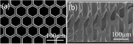
Figure 1. Schematic drawing of the metal-assisted chemical etching (MaCE) process: (a) cleaning the Si (1 0 0) wafer; (b) spin coating photoresist; (c) UV-exposure by MA6; (d) e-beam evaporation of Au; (e) photoresist lift-off; (f) MaCE. (g) The top view of the patterned wafer.
Download figure:
Standard image High-resolution image3. Results and discussion
3.1. Principle of MaCE
In principle, in order to dissolve Si, the following two conditions must be satisfied: (i) the generation of electronic holes from H2O2 in the etched region, (ii) the oxidized Si surface direct contact with the HF solution as shown in figure 2. The following mechanism has been proposed [14]:

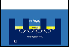
Figure 2. Schematic of transfer during MaCE (the gap between the metal represents the nanoporous morphology of the metal film).
Download figure:
Standard image High-resolution imageThe electronic holes are generated from H2O2, as the HF can only dissolve the Si underneath the Au film, the excess holes diffuse away from the Au film and then oxidize the Si surface between Au film. This oxidized surface will then be etched by HF resulting in the formation of porous defect and the lateral etching effect.
3.2. Suppression of excess holes by H2O2 concentration
The surface qualities corresponding to different H2O2 concentrations are shown in figures 3(a)–(d). In our experiment, the samples were etched for 20 min in aqueous solution with [HF] = 1.8 M and [H2O2] = 0.4, 0.8, 1, 2.55 M, respectively. It can be seen that the Si surface is very smooth when [H2O2] = 0.4 M and the porous defect is more serious in the solution with [H2O2] = 1, 2.55 M. Figure 3(e) shows the etching rate variations with different H2O2 concentration. The etching rate increases with the increasing H2O2 concentration (from 0.4 to 1 M), and then gradually saturates at about 1 M concentration. When the H2O2 supply is abundant, excess electronic holes will oxidize the Si surface and cause the porous defect. It seems reasonable to assume that the concentration of extra electronic holes in the Si decreases with decreasing H2O2 concentration. This assumption is consistent with the results in figure 3(f), which shows that the porous defect decreases with decreasing H2O2 concentration.
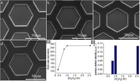
Figure 3. (a)–(d) The SEM images of the etched samples with [HF] = 1.8 M and [H2O2] = 2.55, 1, 0.8, 0.4 M, respectively, and the etch duration was 20 min. (e) Si etch rate for different H2O2concentrations from 0.4 to 2.55 M. (f) Comparison of porous defect density in samples surface.
Download figure:
Standard image High-resolution image3.3. Suppression of lateral etching effect by HF concentration
In order to obtain deeper structures, we extended the etching time. The sample in figure 4(a) was etched for 510 min with [HF] = 1.8 M, [H2O2] = 0.4 M. It can be seen from figure 4(a) that significant etching also occurred in the lateral directions. A similar phenomenon has been observed by Wong et al [19]. This was caused by the excessive holes injected at the metal–silicon interface. These extra electronic holes diffuse away from the metal/Si interface and oxidize the sidewall of the etched structures, leading to the lateral etching effect. So, maybe the lateral etching can be controlled by increasing the HF concentration. This assumption is consistent with the results in figures 4(b) and (c) which shows that the lateral etching decreases with increasing HF concentration. The sample was etched for 510 min and 720 min respectively, with [HF] = 5.4 M, [H2O2] = 0.4 M. However, when the etching time is extended to 720 min as shown in figure 4(c), many randomly-aligned pores are also observed on the sidewall, which may be due to the difficulty of HF transport to the bottom of the etched structures.
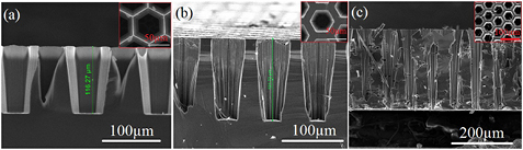
Figure 4. (a) and (b) The cross-sectional SEM images of the etched samples with [H2O2] = 1.8 M and [HF] = 1.8, 5.4 M, respectively; the etch duration was 510 min. (c) The cross-sectional SEM image of the etched samples by [H2O2] = 1.8 M, [HF] = 5.4 M for 720 min.
Download figure:
Standard image High-resolution image3.4. Suppression of randomly-aligned pores effect by ethanol
The wetting agent is often used to improve the etching uniformity, while the effect of the wetting agent on the resulted micro and nano structures morphology receives limited attention [15, 16]. Until now, to the best of our knowledge, the effect of the wetting agent has been only discussed in the fabrication of nanowire and nanostructure arrays. In a study of silicon nanowire formation by MaCE in the HF/H2O2/ethanol mixture using Au mesh as the metal catalyst, Kim et al have reported that the wetting agent can lower the etching rate and influence the etching direction of the resulting morphology [17]. Azeredo et al observed that the external taper angle of nanowires can be controlled by the ethanol concentration [18]. However, bulk micromachining of Si has been challenging for MaCE [19]. In order to reduce the randomly-aligned pores effect, our sample was etched in the etchant solution containing HF/H2O2/ethanol, and the results are shown in figure 5. Compared with figure 4(c), it presents a smoother top surface and sidewall, and the phenomenon of randomly-aligned pores and lateral etching was suppressed efficiently. A possible reason for the improved etching result is that as the etchant solution contains ethanol with low surface tension, and the additional solvent may affect the diffusion and the solubility of the HF and H2O2 in the narrow regions, the mass transfer in the etchant solution with low surface tension improves, resulting in a more vertical and smooth etching.
Figure 5. (a) SEM image of the etched samples using 5.4 M HF–0.4 M H2O2–H2O-Ethanol; the etch duration was 2160 min. (b) Cross-sectional SEM image of the side wall of the same structures.
Download figure:
Standard image High-resolution image
4. Conclusion
In this paper, we present a deep etching method of Si microstructure using metal-assisted chemical etching approach by controlling the concentration and composition of the etchant solution. Honeycomb hole structures have been fabricated with 50 µm width and 280 µm depth. For the etchant solution of HF/H2O2/H2O, the experimental results indicate that the porous defect decreases with decreasing H2O2 concentration and the lateral etching rate decreases with increasing HF concentration. However, high concentration of HF can cause many randomly-aligned pores on the sidewall, which may be due to the increasing difficulty of HF transport inside the etched structures. An ideal surface topography with a smooth sidewall was obtained when the etchant solution contained ethanol. We believe that this method has a potential application in MEMS device fabrication.
Acknowledgment
This work has been supported by NSFC Project (No. 61573346, 61104226), Youth Innovation Promotion Association CAS (2014278), Jiangsu Province Science and Technology Support Program (BE2013056), Jiadong Li thanks the Fund of State key Laboratory of Applied Optics, Changchun institute of Optics, Fine Mechanics and Physics, Chinese Academy of Sciences. Wenhui Lu thanks the Fund of Zhejiang Provincial Natural Science Foundation of China (No. LY15F040002).