
Abstract
The pseudomorphic growth of Ge1−xSnx on Ge causes in-plane compressive strain, which degrades the superior properties of the Ge1−xSnx alloys. Therefore, efficient strain engineering is required. In this article, we present strain and band-gap engineering in Ge1−xSnx alloys grown on Ge a virtual substrate using post-growth nanosecond pulsed laser melting (PLM). Micro-Raman and x-ray diffraction (XRD) show that the initial in-plane compressive strain is removed. Moreover, for PLM energy densities higher than 0.5 J cm−2, the Ge0.89Sn0.11 layer becomes tensile strained. Simultaneously, as revealed by Rutherford Backscattering spectrometry, cross-sectional transmission electron microscopy investigations and XRD the crystalline quality and Sn-distribution in PLM-treated Ge0.89Sn0.11 layers are only slightly affected. Additionally, the change of the band structure after PLM is confirmed by low-temperature photoreflectance measurements. The presented results prove that post-growth ns-range PLM is an effective way for band-gap and strain engineering in highly-mismatched alloys.
Export citation and abstract BibTeX RIS

Original content from this work may be used under the terms of the Creative Commons Attribution 4.0 license. Any further distribution of this work must maintain attribution to the author(s) and the title of the work, journal citation and DOI.
1. Introduction
Ge, similarly to Si, is an indirect band-gap semiconductor and naturally poor light emitter. However, it is possible to tune the band gap and increase the carrier mobility in Ge by alloying with Sn [1]. Moreover, Ge and Sn are group IV elements and can be integrated with the silicon-based complementary metal-oxide semiconductor (CMOS) technology [1, 2]. Hence, Ge1−x Snx alloys are promising materials for future applications in nano- [3] and optoelectronics [4]. For the Sn concentration in the range of a few atomic percent, significant enhancement of the carrier mobility is observed [5, 6]. When the Sn concentration in crystalline and fully relaxed Ge1−x Snx alloys increases above 8–10 at.%, the alloy becomes a direct band gap semiconductor [7]. Unfortunately, the equilibrium solid solubility of Sn in Ge is limited to about one atomic percent [8]. Therefore, there is a need to use non-equilibrium fabrication processes to incorporate larger amounts of Sn into Ge and avoid its segregation. Promising methods to fabricate Ge1−x Snx alloys are molecular-beam epitaxy (MBE) [9–11], chemical vapour deposition (CVD) [12, 13], and ion implantation followed by non-equilibrium annealing like ns-range pulsed laser melting (PLM) [14] or the ms-range flash-lamp annealing [15]. Wirths et al demonstrated the first group-IV laser using a Ge1−x Snx alloy grown on Ge substrates by CVD [4]. The direct band-gap transition was obtained for a Sn concentration of about 13 at.%, and the fabricated laser operates at a wavelength of 2.3 µm. Du et al showcased an optically pumped Ge1−x Snx laser operating at 260 K [16]. Zhou et al have demonstrated electrically injected Ge1−x Snx lasers on Si operating up to 100 K [17]. Normally, Ge1−x Snx alloys grown epitaxially on Ge substrates are compressively strained, and the strain increases with increasing the amount of Sn. The compressive strain has two main disadvantages: (a) it shifts the transition from indirect (L point) to direct (Г point) band gap to higher Sn concentration and (b) it reduces the carrier mobility [18]. The strain can be released by nanostructuring the grown layer. Elbaz et al fabricated Ge1−x Snx -based microdisks for group-IV lasers [13]. While the as-grown Ge1−x Snx layer was a compressively strained indirect band-gap semiconductor, after nanostructuring, the compressive strain was released and a direct band-gap material was achieved for a Sn concentration of as low as 5.4 at.% [13].
In this article, we present effective band-gap and strain engineering in Ge1−x Snx (x ⩽ 0.11) alloys via the ns-range liquid phase epitaxy using a post-growth PLM. As revealed by micro-Raman and x-ray diffraction (XRD), the in-plane compressive strain in Ge1−x Snx layer is released after the post-growth melting with a pulsed laser energy density higher than 0.20 J cm−2. Moreover, the layer becomes tensile strained when the pulsed laser energy density increases to 0.5 J cm−2. This strain transition from compressive to tensile is also confirmed by XRD for PLM energy density between 0.4 and 0.5 J cm−2. We show that the thickness of the Ge1−x Snx layer with released strain depends on the energy density of the laser pulse. The presented post-growth PLM can be applied for the fabrication of strain relaxed or even tensile strained virtual substrates for the growth of strain free Ge1−x Snx layers with a high Sn concentration.
2. Experimental part
2.1. Material fabrication
Ge1−x Snx layers with a Sn concentration of 11% were epitaxially grown on (100) oriented 4 inch p-type Si substrates with a sheet resistance of ρ = 10–20 Ω cm by MBE at the Institute of Semiconductor Engineering, University of Stuttgart. The MBE process starts with a thermal desorption step at a substrate temperature of TS = 900 °C to remove the native SiO2 and therefore to prepare the substrate surface for the consecutive epitaxy. First, a 50 nm thick Si buffer layer was grown at a substrate temperature of TS = 600 °C. Next, the substrate temperature was reduced to TS = 330 °C and a 100 nm thick Ge layer was grown. Afterwards, a thermal annealing step at TS = 830 °C for a duration of t = 5 min allows threading dislocations to annihilate and is used to form a virtual Ge substrate (Ge-VS). An additional 300 nm thick Ge buffer layer was grown on top and annealed at TS = 750 °C for t = 5 min. Finally, a 290 nm thick Ge1−x Snx layer was grown on top of the Ge buffer layer at TS = 120 °C.
The band gap and strain engineering of the epitaxial Ge1−x Snx layers was performed by PLM for 28 ns using a XeCl excimer laser with 308 nm wavelength. The energy density of the laser pulse varied from 0.2 to 0.6 J cm−2. The homogeneously irradiated area was 5 × 5 mm2. The annealing was done at atmospheric condition.
2.2. Characterisation of materials
The influence of the PLM process on the microstructural, electrical, and optical properties of the Ge1−x Snx alloys was studied using micro-Raman spectroscopy, high-resolution x-ray diffraction (HRXRD), Rutherford backscattering spectrometry in random (RBS/R) and channelling (RBS/C) directions, transmission electron microscopy (TEM) and low-temperature photoreflectance (LT-PR) spectroscopy.
Micro-Raman spectroscopy was performed on a Horiba LabRam n°1/24 h system equipped with Nd:YAG laser with a wavelength of 532 nm and a liquid-nitrogen-cooled charge-coupled device (CCD) camera. All measurements were performed in backscattering geometry with the laser power of 1 mW focused on a circular area with 1 µm diameter. The phonon spectra were recorded in the wavenumber range of 50–550 cm−1.
HRXRD was performed with a Rigaku SmartLab x-ray diffractometer system. Three different types of measurements were carried out on each of the samples: polycrystal analysis, rocking curve (RC) measurements and reciprocal space map (RSM) measurements. The polycrystal analysis is a one-dimensional 2 theta scan with a fixed incident angle ω = 3°, which is fixed near the critical angle. The RC measurement is a one-dimensional scan and measures diffraction intensity distributions along a reciprocal lattice vector. With this measuring method (2 theta/omega scan), the symmetrical (004) reflection for the Ge1−x Snx layers on a Si (100) substrate was investigated. The RSM measures diffraction intensity distributions by scanning both the diffraction angle and sample rotation. The asymmetrical (−2–24) reflections of the samples were measured using the RSM method. The lateral and vertical lattice constants can be determined from the RC and RSM results.
RBS/R and RBS/C experiments were performed at the Ion Beam Center of the Helmholtz-Zentrum Dresden-Rossendorf using its 2 MV van de Graaf accelerator. The He+ beam had an energy of 1.7 MeV with a diameter of about 1 mm. The RBS measurements were used to determine the thickness and composition of the grown Ge and Ge1−x Snx layers. The obtained RBS spectra were fitted with the Software SIMNRA [19].
TEM investigations of the as-grown and pulsed-laser-molten samples were done in cross-sectional geometry using a Titan 80–300 microscope (FEI) operated at an accelerating voltage of 300 kV. High-angle annular dark-field scanning TEM imaging and spectrum imaging analysis based on energy-dispersive x-ray spectroscopy (EDXS) were performed at 200 kV with a Talos F200X microscope equipped with a Super-X EDX detector system (FEI). Prior to TEM analysis, the specimen mounted in a high-visibility low-background holder was placed for 10 s into a Model 1020 Plasma Cleaner (Fischione) to remove potential contamination.
The direct optical transitions in as-grown and annealed films were determined by LT-PR measurements at 30 K in a 'bright configuration' experimental setup. Samples were excited by continuous-wave 405 nm laser of 100 mW power chopped with the frequency of 280 Hz. A phase sensitive detection of the LT-PR signal is accomplished using a lock-in amplifier. This measurement was performed at Wroclaw University of Science and Technology.
3. Results and discussion
3.1. Investigation of the microstructure
The microstructure and element composition of the as-grown and PLM-treated samples were investigated using cross-sectional TEM-based analysis. Figure 1(a) depicts a representative bright-field TEM image of the Ge0.89Sn0.11 layer grown on a Ge virtual substrate. To record this bright-field TEM image, the TEM specimen was oriented in Si ![$\left[ {1\bar 10} \right]$](https://content.cld.iop.org/journals/0953-8984/35/5/055302/revision3/cmaca3eaieqn1.gif) zone axis geometry relative to the electron beam. While the Ge virtual substrate is characterised by a uniform contrast (besides the presence of some dislocations close to the Si substrate), the Ge0.89Sn0.11 layer shows a columnar signature, particularly in the upper three quarters of the film. Comparing with the EDXS-based element analysis in figure 1(b), this columnar contrast seems to arise from a slightly varying Sn distribution in the as-grown Ge0.89Sn0.11 layer. Regarding the microstructure, the Ge–Sn film grows epitaxially on the Ge virtual substrate, as derived from the fast Fourier transform (FFT, depicting a
zone axis geometry relative to the electron beam. While the Ge virtual substrate is characterised by a uniform contrast (besides the presence of some dislocations close to the Si substrate), the Ge0.89Sn0.11 layer shows a columnar signature, particularly in the upper three quarters of the film. Comparing with the EDXS-based element analysis in figure 1(b), this columnar contrast seems to arise from a slightly varying Sn distribution in the as-grown Ge0.89Sn0.11 layer. Regarding the microstructure, the Ge–Sn film grows epitaxially on the Ge virtual substrate, as derived from the fast Fourier transform (FFT, depicting a ![$\left[ {1\bar 10} \right]$](https://content.cld.iop.org/journals/0953-8984/35/5/055302/revision3/cmaca3eaieqn2.gif) zone axis pattern) of the representative high-resolution (HRTEM) image in figure 1(c). At the border regions between the columns, there are no defects visible.
zone axis pattern) of the representative high-resolution (HRTEM) image in figure 1(c). At the border regions between the columns, there are no defects visible.
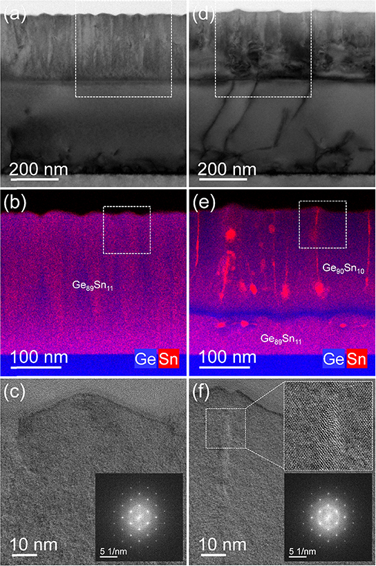
Figure 1. Cross-sectional TEM-based analysis of (a)–(c) the as-grown sample and (d)–(f) after PLM treatment with an energy density of 0.5 J cm−2. (a), (d) Representative bright-field TEM images. (b), (e) Superimposed Ge (blue) and Sn (red) element distributions obtained for the regions marked with a dashed white square in (a), (d). The given compositions were determined by EDXS-based quantification. (c), (f) HRTEM images for the regions marked with a dashed white square in (b), (e). In each panel, the corresponding fast Fourier transform of the complete HRTEM image is shown in the lower right corner. In panel (f), the enlarged view of the Sn-enriched location is shown as inset in the upper right corner.
Download figure:
Standard image High-resolution imageAfter PLM with an energy density of 0.5 J cm−2, the columnar signature changed and the sample surface morphology is restructured (figure 1(d)). Comparing the superimposed Sn and Ge element maps in figures 1(b) and (e), it can be concluded that PLM leads to a slight Sn redistribution. In particular figure 1(e) shows the separation of the original Ge0.89Sn0.11 layer into three regions: from top to bottom (a) the Ge0.89Sn0.11 film molten during PLM, (b) an almost pure Ge layer as interface between molten and non-molten region, and (c) the residual Ge0.89Sn0.11 film not molten during PLM. Besides Sn-rich cluster formation, the molten region shows Sn-rich filaments, reaching up to the sample surface. Both features may be the combined effect of a slightly varying Sn distribution already in the as-grown sample and an enhanced Sn diffusion during PLM. It should be mentioned that a wall-like structure, having its plane normal perpendicular to the normal of the TEM lamella plane, may also appear as filament in a two-dimensional TEM-based projection image. Similar filament structures have been observed after laser annealing of Ge1−x
Snx
[20]. Their origin is still under discussion [20]. Beside small Sn segregation, the molten layer has a comparable composition (Ge0.90Sn0.10) and similar structural properties as the as-grown sample, i.e. it is of single-crystalline nature. In particular, the FFT analysis of the HRTEM image in figure 1(f) leads to a ![$\left[ {1\bar 10} \right]$](https://content.cld.iop.org/journals/0953-8984/35/5/055302/revision3/cmaca3eaieqn3.gif) zone axis pattern comparable to the one given in the inset of figure 1(c). However, there may be some defect structures at the Sn-enriched locations, as exemplarily shown in the enlarged part of the HRTEM image depicted in the upper right inset of figure 1(f).
zone axis pattern comparable to the one given in the inset of figure 1(c). However, there may be some defect structures at the Sn-enriched locations, as exemplarily shown in the enlarged part of the HRTEM image depicted in the upper right inset of figure 1(f).
By varying the energy density of the pulse laser, we can control the thickness of the molten layer, as shown in figure 2. Taking into account the mass density in Ge1−x Snx , the atomic thicknesses of the molten layer were determined from RBS/R data (see supplementary materials S1). Melting of Ge0.89Sn0.11 was observed already at an energy density of 0.25 J cm−2, and the thickness of the molten layer increases with increasing the energy density of the laser pulses. The estimated temperature during PLM with 0.25 J cm−2 is in the range of 900 °C. This temperature corresponds to the melting point of Ge1−x Snx with about 10% of Sn [21]. There is an almost linear dependence between the thickness of the molten layer and the energy density (see red regression line in figure 2). The conversion from the extracted melting depth in atoms cm−2 by SIMNRA into melting depth in nm leads to about 13% thinner Ge1−x Snx layers. This error was determined by comparing the RBS/R (supplementary materials S1(a)) and TEM (figure 1) results of the as grown state. The error comes from the not well determined mass density of the Ge1−x Snx alloy grown by MBE and the mass approximation by Vegard's law. After PLM, the mass density is getting inconstant due to the atoms and strain redistributions

Figure 2. The physical and calculated thicknesses of the molten Ge1−xSnx layer as a function of the energy density of the laser pulses.
Download figure:
Standard image High-resolution image3.2. Optical properties and strain engineering
In more details the microstructural properties of the Ge and Ge1−x Snx layers, i.e. the crystallographic orientation and strain, were studied by HRXRD, µ-Raman spectroscopy and PR measurements. Figure 3(a) shows the high-resolution RC obtained from the samples in as-grown state and after PLM with energy densities of 0.4, 0.5 and 0.6 J cm−2. The as grown state shows three XRD peaks located at about 64.18°, 66.07° and 69.13° corresponding to Ge0.89Sn0.11, the Ge-virtual substrate and the Si substrate, respectively. After PLM the GeSn peak is divided in two peaks located at 64.22° and 65.24° for 0.5 J cm−2 (see figure 3(a)) because of the relaxation of the top layer. In figure 3(b) the polycrystal analysis is depicted. The 2θ scan exhibits one sharp peak at about 38.08° in the as-grown state and 38.18° after PLM with 0.5 J cm−2, which can be due to some Sn segregation visualised in the cross-sectional TEM image taken from the as-grown sample (see figure 1(a)) or some inclusions of small nanocrystals. The absence of other well distinguishable peaks confirms the epitaxial growth of Ge1−x Snx alloy on the Ge-virtual substrate. Additionally, it can be concluded that PLM does not change the crystal quality because the polycrystal analyses before and after annealing are very similar.

Figure 3. HRXRD rocking curve (a) and polycrystal analyses (b) of the Ge1−xSnx sample in as-grown state and after PLM with energy densities with 0.4, 0.5 and 0.6 J cm−2. In order to distinguish between the curves a visualisation offset with increasing energy densities is applied.
Download figure:
Standard image High-resolution imageFigure 4 shows the space mapping results of as-grown (a) and PLM 0.4 J cm−2 (b), PLM 0.5 J cm−2 (c) and PLM 0.6 J cm−2 (d) samples. For a better visualisation, the reciprocal coordinates were transformed in coordinates of the real space. Using the real space, both the in-plane a|| and out-of-plane a⊥ lattice parameters can be determined. Details about the calculation of a0, a|| and a⊥ can be found elsewhere [22]. By comparing the lattice parameter for relaxed Ge1−x
Snx
alloy a0 for known Sn content with our experimental results, the in-plane strain  || XRD can be calculated by equation (1)

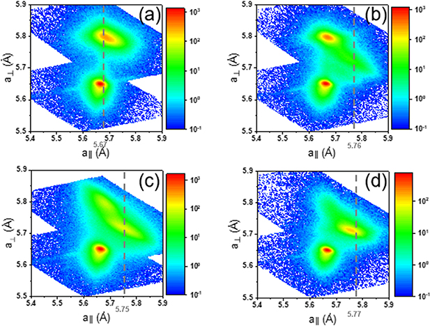
Figure 4. HRXRD space mapping with in-plane a|| and out of plane a⊥ lattice parameters for (a) as-grown and annealed samples with an energy density of (b) 0.4, (c) 0.5 and (d) 0.6 J cm−2. Additionally, the calculated in-plane lattice parameter obtained from the µ-Raman results (from table 2) are included with dashed grey lines. For a better visualisation, the reciprocal lattice parameter unit q was transferred into cell dimension units using a⊥ = 8π/q⊥ and a|| =  2π/q||.
Download figure:
Standard image High-resolution imageThe obtained values are summarised in table 1. The a|| and a⊥ for the as-grown Ge-virtual substrate are 5.6647 and 5.6503 Å, respectively, while the tabulated value for relaxed Ge is 5.6575 Å [23]. This means that the virtual substrate is slightly strained by || XRD = 0.009. In the as-grown sample, the GeSn peak is shifted to a larger a|| value compared to the Ge-virtual substrate peak. The in-plane lattice parameter of GeSn is a|| = 5.6928 Å, but the calculated value of a0 for relaxed Ge0.9Sn0.1 is 5.7502 Å. Hence, our Ge0.9Sn0.1 layer in as-grown state is under compressive strain || XRD = −0.010 because of pseudomorphic growth of Ge0.9Sn0.1 on Ge-virtual substrate. The a⊥ for as-grown Ge0.9Sn0.1 is 5.7944 Å due to the out-of-plane tensile strain. After PLM with 0.5 J cm−2 the new a|| and a⊥ from the top layer are 5.7478 and 5.7190 Å, respectively, while the lattice parameters from the non-molten layer remain almost unchanged. The in-plane strain is changed from compressive || XRD = −0.0100 in the as-grown sample to tensile || XRD = 0.0028 after PLM with an energy density of 0.5 J cm−2 and to || XRD = 0.0038 after PLM at 0.6 J cm−2. The Ge0.904Sn0.096 layer after PLM with 0.4 J cm−2 is still in plane compressive strained with || XRD = −0.0003, but strain is reduced compared to the as grown state. The a0 for top Ge1−x
Snx
layer is a bit different due to Sn redistribution after PLM (see figure 1(d)).
Table 1. HRXRD in-plane a|| and out-of-plane a⊥ lattice parameters and ||XRD strain calculated for as-grown and PLM-treated samples with their composition dependant relaxed lattice parameter a0. Geas-grown and GeSnas-grown belong to the material in the as grown state. The results of GeSn pertain to the not effected material by PLM (see figure 1(e)). GeSnPLM-0.4, GeSnPLM-0.5 and GeSnPLM-0.6 are samples annealed with 0.4, 0.5 and 0.6 J cm−2, respectively. The accuracy of the out of plane lattice parameter a⊥ is ±0.0001 Å and in plane a|| ±0.001 Å.
| Sn (at.%) | a|| (Å) | a⊥ (Å) | a0 (Å) |
|| XRD
| |
|---|---|---|---|---|---|
| Geas-grown | — | 5.665 | 5.6503 | 5.6575 | 0.0009 |
| GeSnas-grown | 11.1 ± 0.5 | 5.693 | 5.7944 | 5.7502 | −0.0100 |
| GeSn | 10.2 ± 0.5 | 5.681 | 5.7907 | 5.7430 | −0.0108 |
| GeSnPLM-0.4 | 9.6 ± 0.5 | 5.736 | 5.7394 | 5.7380 | −0.0003 |
| GeSnPLM-0.5 | 8.9 ± 0.5 | 5.748 | 5.7190 | 5.7316 | 0.0028 |
| GeSnPLM-0.6 | 8.9 ± 0.5 | 5.754 | 5.7149 | 5.7318 | 0.0038 |
Table 2. Strain calculation by using the LO-Ge–Ge phonon mode. ωGeSn-measurment is the obtained peak position of the samples after Lorentz fitting and ΔωGeSn-alloy relaxed is the expected peak shift due to alloying Ge with Sn according to equation (3). The Sn concentration xSn is obtained by XRD. As a comparative value the in plane strain || XRD was obtained from table 1. The accuracy of the measured LO-Ge–Ge phonon mode is 0.1 cm−1.
| Sample | ωGeSn-measurement (cm−1) | ΔωGeSn-alloy relaxed (cm−1) | Δωstrain (cm−1) | xSn (at.%) |
|| Raman
|
|| XRD
|
|---|---|---|---|---|---|---|
| As grown | 296.2 | −9.2 | 5.0 | 11.1 ± 0.5 | −0.0132 | −0.0100 |
| PLM-0.4 J cm−2 | 291.2 | −8.0 | −1.3 | 9.6 ± 0.5 | 0.0035 | −0.0003 |
| PLM-0.5 J cm−2 | 290.6 | −8.5 | −1.4 | 10.2 ± 0.5 | 0.0038 | 0.0028 |
| PLM-0.6 J cm−2 | 290.7 | −7.4 | −2.4 | 8.9 ± 0.5 | 0.0064 | 0.0038 |
In order to validate the HRXRD results and investigate the in-plane strain distribution of the as-grown and the annealed states, µ-Raman measurements are performed. Figure 5 shows the µ-Raman spectra obtained from the Ge0.89Sn0.11 samples before and after PLM with energy densities between 0.2 and 0.6 J cm−2.

Figure 5. Normalised µ-Raman spectra for the Ge–Ge longitudinal optical phonon mode of the as-grown and PLM treated Ge1−x Snx alloys with energy densities of 0.20, 0.25, 0.30, 0.35, 0.40, 0.50 and 0.60 J cm−2. The Raman spectrum of Ge is shown for reference. The peak position of each spectra was fitted with Lorentzian peak function.
Download figure:
Standard image High-resolution imageThe Ge–Ge longitudinal optical (LO) phonon mode in relaxed Ge ωGe is at 300.5 ± 0.1 cm−1, as also seen in the figure 5 [24]. Due to the pseudomorphic growth of Ge0.89Sn0.11 epitaxial on a Ge-virtual substrate with a smaller lattice parameter, the Ge0.89Sn0.11 layer is compressively strained. Hence, the Ge–Ge phonon mode in as-grown Ge0.89Sn0.11 is located at 296.6 cm−1 instead of 291.3 cm−1. The PLM process leads to strain relaxation and a slight Sn redistribution within the annealed Ge1−x
Snx
layer. This strain relaxation is visible as the shift of the Ge–Ge phonon mode after PLM towards lower wavenumber. The sample annealed with 0.20 J cm−2 has only a slight red shift because the laser energy is close to the melting threshold. This can be confirmed by the RBS/R spectra revealing the same Sn distribution like in the as-grown sample (see supplementary materials S1(a)). All other samples annealed with the pulsed laser energy densities of 0.25 J cm−2 and higher show the main Ge–Ge phonon mode at about 290 ± 1 cm−1. The penetration depth of the green laser in Ge, used for sample excitation in the micro-Raman spectroscopy, is approximately 20 nm from the surface [25]. Due to alloying with Sn, the penetration depth of the green laser in Ge1−x
Snx
layer can be even smaller. Hence, the detected micro-Raman spectra can be used to determine the strain distribution in the top layer of about 15 nm thick only. The measured phonon peak position is influenced by the composition of the Ge1−x
Snx
alloy Δωalloy and the strain Δωstrain. This can be expressed by equation (2). Δωalloy is influenced by (a) the different mass Δωmass of the Ge and Sn atoms in the alloy and (b) the change of bond length Δωbond between Ge atoms due to alloying with Sn. Since the strain, mass difference and bond length depend linearly on the concentration of Sn, the value for Δωalloy can be calculated with equation (3). By using the disorder parameter b, which is reported as b = −83.11 [26], the Raman shift in a fully relaxed Ge1−x
Snx
with a low concentration of Sn can be calculated. The shift due to the in-plane strain || Raman can be calculated using equation (4). The strain coefficient c = −374.53 [26] was used


Since there is no contribution of the Sn rich filaments to the Raman spectra, the in-plane strain || Raman can be calculated by using equation (4). The results for the as grown state and the PLM samples with 0.4, 0.5 and 0.6 J cm−2 are shown in table 2.
By comparing the results of the in-plane strain from HRXRD || XRD with the µ-Raman results in table 2, we can conclude that the Ge1−x
Snx
layer is compressively strained before annealing and tensile strained after annealing. In fact, the strain obtained by XRD and Raman for the PLM samples are different, but this can be explained with the different penetration depths of the methods. With µ-Raman we get signals only from the top ca. 15 nm and with XRD one measures the whole layer. Additionally, the disorder parameter b and the strain coefficient c are determined for Ge1−x
Snx
alloys with x = 0.025 and 0.077 [26]. In our case, the Sn concentration is significantly higher. Therefore, slight differences can be expected. Further, by converting the in-plane strain into in-plane lattice parameter and adding this value in figure 4 it is visible that some surface generated tail regions of the Ge1−x
Snx
RSM matches the Raman results.
The change of the fundamental optical transition in Ge1−x Snx alloys after PLM with 0.4 and 0.5 J cm−2 is determined by PR spectroscopy. The results of the measurements are displayed in figures 6(a)–(c). The obtained low temperature PR signal is fitted with the low-field electromodulation Lorentzian line-shape function form known as the Aspnes formula equation (5) [27]

Figure 6. Photoreflectance spectra of the samples: (a) in the as grown state, (b) after PLM with 0.4 J cm−2, and (c) after PLM with 0.50 J cm−2 and (d) optical transition energies as function of in-plane strain. (a)–(c) Experimental results are marked by solid black lines. Curves fitted to the strongest resonances are depicted by coloured solid lines and are related to optical transitions in Ge (blue) and Ge1−xSnx (red and purple). Moduli of each single resonance are presented by area charts below the corresponding fitted lines with the value scale same as for photoreflectance. The moduli are plotted with an offset, such that zero value is on the bottom of each chart. (d) Energies related to observed resonances are depicted by squares. Calculated energies of optical transitions involving heavy holes (solid lines) and light holes (dashed lines) are plotted for Ge0.89Sn0.11 (red) and for Ge0.92Sn0.08 (purple) alloys.
Download figure:
Standard image High-resolution image
where  is the energy dependence of PR signal, n is the number of PR resonances used to simulate PR signal,
  is the photon energy of the probe beam, Ej
is the energy of optical transition, and Γj, Cj
and θj
are the broadening, amplitude and phase angle of PR resonance, respectively. At 30 K, the nature of optical transitions (PR resonances) in Ge1−x
Snx
alloys is excitonic and therefore the exponent mj
is assumed to be 2. The fitting curves are plotted in figures 6(a)–(c) by colour lines together with the moduli of the individual PR resonances (colour lines with filling), which are obtained from the equation (5) with parameters derived from the fit according to the equation (6)
is the photon energy of the probe beam, Ej
is the energy of optical transition, and Γj, Cj
and θj
are the broadening, amplitude and phase angle of PR resonance, respectively. At 30 K, the nature of optical transitions (PR resonances) in Ge1−x
Snx
alloys is excitonic and therefore the exponent mj
is assumed to be 2. The fitting curves are plotted in figures 6(a)–(c) by colour lines together with the moduli of the individual PR resonances (colour lines with filling), which are obtained from the equation (5) with parameters derived from the fit according to the equation (6)
So far, the Aspnes formula has been widely used to analyse electro-reflection spectra in a variety of semiconductor materials, including GeSn [28–30]. The dependence of the energies extracted from the spectra on the in-plane strain || XRD, given in table 1, is shown in figure 6(d). Resonances at around 0.86 and 1.14 eV are related to optical transitions in the Ge layer beneath the Ge0.89Sn0.11 layer. The resonance at 0.86 eV is associated with the direct band gap of Ge [31], while the resonance at 1.14 eV is separated from it by the value of spin–orbit split-off energy of Ge [27]. The energies assigned to resonances at around 0.55 eV for as-grown samples are in good agreement with the values calculated for Ge0.89Sn0.11 at 30 K when the lateral compressive strain of −1% is applied. Therefore, the PR resonance at 0.51 eV is attributed to the optical transition between the heavy-hole band and the conduction band, while the resonance at 0.58 eV is attributed to the optical transition between the light-hole band and the conduction band. The effect of strain on the band gap is also known from strain investigations on Ge [32]. It is worth noticing that these resonances may show a Franz–Keldysh oscillation [27], which complicates the analysis of PR spectra with two Aspnes resonances and the determination of the optical transition at higher energy (light-hole and heavy-hole transition, respectively, in the case of compressive and tensile strain). Therefore, clear interpretation of the optical transition energies for Ge1−x
Snx
(around 0.55 eV) in the samples after PLM is difficult, due to both the more complex structure of the materials after the melting process and the possible Franz–Keldysh oscillations in the measured spectra. Nevertheless, these spectra are fitted with two resonances and the obtained values undoubtedly support simultaneous change of the average content of Sn in the alloy and the reduction of the in-plane compressive strain such that the tensile strain can be observed, see figure 6(d).
4. Conclusions
Single crystalline Ge0.89Sn0.11 on Ge-virtual substrate could be successfully grown by MBE. Due to the pseudomorphic growth, the Ge0.89Sn0.11 alloy is under compressive strain. Using post-growth PLM, efficient strain engineering can be achieved for Ge1−x Snx alloys. Therefore, the ns-range PLM combined with MBE can be an effective approach for growing strain-free Ge1−x Snx layers with Sn-concentration up to 11 at.%. The Ge0.89Sn0.11 alloy begins to melt at energy densities between 0.20 J cm−2 and 0.25 J cm−2 and the melting depth depends linearly on the used energy density of ns-laser pulse. Energy densities higher than 0.5 J cm−2 converts the in-plane compressive strain to tensile strain. After PLM, the Ge1−x Snx layer is single crystalline with small redistributions of Sn. Due to the strain in the Ge1−x Snx layers, the valence band is divided in light and heavy holes. In case of the compressively strained as grown material, an optical transition between heavy holes to the conduction band takes place at 0.51 eV. In contrast after PLM in the tensely strained material, the transition occurs at around 0.52 eV (0.5 J cm−2) and 0.53 eV (0.4 J cm−2), respectively. This is explained by the change of strain and Sn concentration in the molten layer.
Acknowledgments
The authors thank Romy Aniol for TEM specimen preparation. Furthermore, the use of the HZDR Ion Beam Center TEM facilities and the funding of TEM Talos by the German Federal Ministry of Education and Research (BMBF), Grant No. 03SF0451, in the framework of HEMCP are acknowledged. This work was supported by the Bundesministerium für Bildung und Forschung (BMBF) under the project 'ForMikro': Group IV heterostructures for high performance nanoelectronic devices (SiGeSn NanoFETs) (Project-ID: 16ES1075). We gratefully acknowledge the HZDR Ion Beam Centre for their support with RBS.
Data availability statement
All data that support the findings of this study are included within the article (and any supplementary files).
Supplementary data (0.5 MB PDF)