
Abstract
This paper describes the development of flexible energy harvesters using PVDF–graphene nanocomposites. Nanocomposite films are prepared by simple solution casting of polyvinylidene fluoride/graphene oxide (PVDF/GO) solution. PVDF/reduced graphene oxide (PVDF/RGO) films are produced by in situ thermal reduction of PVDF/GO films. The effects of the presence of GO and RGO on the characteristics of the PVDF are examined through scanning electron microscopy (SEM), energy dispersive spectroscopy (EDS), Fourier transform infrared spectroscopy (FTIR) and x-ray diffraction (XRD) measurements. The ferroelectric behavior and dielectric constant of the nanocomposite show remarkable increase compared to those of pure PVDF for a value of 0.1 wt% of GO loading. The PVDF/RGO film-based energy harvesting (EH) device generates higher energy compared to those of PVDF and PVDF/GO films. The nanocomposite EH device scavenges a maximum power of 36 nW against a load resistance of 704 kΩ.
Export citation and abstract BibTeX RIS
1. Introduction
A piezoelectric material generates electrical charge from mechanical stress, referred to as 'the direct piezoelectric effect', and produces mechanical strain from an electrical field, 'the converse piezoelectric effect'. The direct piezoelectric effect is very effective in structural measurement, pressure sensors and vibrational energy scavenging, while the converse piezoelectric effect is utilized for active vibrational dampening, shape control, and actuation [1, 2]. Lead zirconate titanate (PZT), zinc oxide (ZnO) and PVDF are representative piezoelectric materials used in microelectromechanical system (MEMS) piezoelectric transducers [3]. Most previous piezoelectric work has focused on PZT due to its high piezoelectric coefficient. The main problems of PZT come from its toxicity and brittleness [4]. ZnO nanowires can generate decent values of energy outputs with which light emitting diodes (LEDs) are powered [5–7]. However, the structural length of these nanowires is around a few micrometers which could limit their energy harvesting capacity. Furthermore, the manufacturing process is very complicated due to the high processing temperature and difficulty in controlling the orientation of individual wires [8]. Polymer-based piezoelectric materials could be an alternative approach.
The discovery of piezoelectricity in polyvinylidene fluoride (PVDF) by Kawai in 1969 introduced a highly flexible and processable material [9]. The piezoelectricity of PVDF allowed for the development of a relatively new class of elastically compliant, low dielectric materials, referred to as electroactive polymers (EAPs). However, their low voltage and force generation capabilities have greatly constrained their applications [10]. To overcome the shortcomings of current EAPs, notably PVDF, inorganic fillers with high dielectric permittivity, such as ceramic powders, barium titanate (BaTiO3), lead titanate (PbTiO3), lead zirconate titanate (PZT) and lead magnesium niobate–lead titanate (PMN–PT) have been incorporated into PVDF matrices. However, the dielectric permittivity of PVDF composites is still not high enough, even at high concentration of ceramic filler [11–15]. The weak interfacial interaction and pores in composites might be responsible for the low dielectric permittivity of the composites. Moreover, the use of ceramic fillers deteriorates the flexibility of the polymer matrix due to the high concentration of the rigid ceramic particles [11–15].
Apart from electrical properties, carbon nanotubes (CNTs) also impart better mechanical properties to composites at relatively low filler content. CNT-based composites offer superior dielectric properties because of the higher surface area and larger aspect ratios of nanotubes [16, 17]. However, the agglomeration of CNTs and their compatibility with polymer matrices are the primary concerns of researchers in this field. Although different strategies such as modification of nanotubes are still being investigated, overcoming these problems remains a significant challenge in this field [18].
Single layer graphite, known as graphene, has attracted considerable scientific interest in recent years owing to its outstanding mechanical, thermal and electrical properties as well as large surface area [19–21]. Thus, graphene has been considered to be an ideal nanofiller for improving the mechanical, electrical and thermal properties of polymers [22]. Most of the research in the field has focused on graphene oxide (GO) or the reduction of GO (RGO) prior to its dispersion into polymer. These nanocomposites produce multilayer platelets rather than single layer sheets [23, 24]. Tang et al first demonstrated that solution cast film can be thermally reduced without employing any hazardous reducing agents, like dimethylhydrazine [25]. Isolated single layer RGO was found to enhance the thermal and electrical properties at very low percolation values. However, no comprehensive study of piezoelectric enhancement of this composite film has been reported.
In this paper, nanocomposites of PVDF and GO (PVDF–GO) and in situ thermal reduction of GO (PVDF–RGO) are analyzed in terms of the ferroelectric behavior and enhancement mechanism. The analysis provided herein also explores the changes in the PVDF film characteristics, the phase transition, the relative dielectric constant and the dielectric loss with a very low GO loading. A comprehensive study of the energy scavenging capability of PVDF and its composites is also discussed.
2. Experimental section
2.1. Preparation of GO
GO was prepared from graphite powder according to the Hummers and Offman (1958) method, as described elsewhere [26]. Extra pure graphite powder (2.0 g, Merck, 12.0 g mol−1, 99.5%) was pre-oxidized by slowly adding it to a solution of sulfuric acid (H2SO4, 50 ml, Dongwoo fine-chem, 95%–97%) and nitric acid (HNO3, 50 ml, Dongwoo fine-chem, 68%–70%) followed by stirring at 80 ° C for 4 h. The mixture was cooled down to room temperature and then washed with de-ionized water until the pH value was neutral, followed by drying at 40 ° C overnight. The resultant pre-oxidized graphite was dispersed into cold concentrated H2SO4 in a reaction vessel, which was kept in an ice bath and stirred followed by slow addition of potassium permanganate (KMnO4, 10 g, Sigma Aldrich, 97%). The temperature was held below 10 ° C during the addition. The mixture was stirred at 35 ° C for 2 h, during which time the solution thickened and turned a brownish gray in color. Then, 250 ml of de-ionized water was added and the temperature was raised to 100 ° C for 15 min. Over this time, the solution became brown in color. The addition of 700 ml of de-ionized water with 30 ml of hydrogen peroxide (H2O2, Dongwoo fine-chem, 30%) followed by stirring for 1 h removed the Mn+ ions, resulting in a yellow-brown colored solution. The solid product collected from the solution after 12 h was washed with 5% hydrochloric acid (HCl) until sulfate ions were no longer detectable with barium chloride (BaCl2). Then the sample was re-dispersed in de-ionized water five times in order to remove the impurities. Further centrifugation at 3000 rpm for 5 min was carried out to remove all visible particles from the precipitate (unexfoliated GO). The supernatant was then subjected to high-speed centrifugation at 10 000 rpm with a g force of 12 298 for 10 min, and the resulting sediment was dried at 60 ° C in a vacuum oven to yield GO powder.
2.2. Preparation of polymer nanocomposites
Solef PVDF 21 510 was supplied by Solvay Korea Co. N-N dimethylformamide (DMF, anhydrous 99.8%) was purchased from Sigma Aldrich. The dried GO powder was dispersed in DMF solvent (1 mg ml−1) and ultra-sonicated for 2 h below 60 ° C, as the flash point of DMF is around 60 ° C. PVDF powder (2.5 g) was separately dispersed in 50 ml of DMF under magnetic stirring for 2 h at 30 ° C. Then, a GO/DMF solution with 0.1 wt% of GO was added to the PVDF/DMF solution. 0.1 wt% of GO was chosen because it is possible to obtain the purely piezoelectric β-polymorph at this concentration level [27]. Good dispersion of GO in PVDF was achieved after 5 min of ultra-sonication. The nanocomposite solution was stirred at 500 rpm at 60 ° C for 1 h to achieve good dispersion and interaction of the GO with the PVDF. The nanocomposite solution was then placed on a glass substrate and cast using a film casting knife. The films were kept in a vacuum oven overnight at 70 ° C to evaporate the solvent. Three different films were made: one with only PVDF and two films with PVDF/GO. One of the PVDF/GO films was subjected to a hot press at 150 ° C for 2 h, well below the melting temperature of PVDF, in an effort to avoid altering the dispersion of GO. The PVDF/GO nanocomposite synthesis method and further in situ thermal reduction process at 150 ° C to obtain PVDF/RGO nanocomposite helped to produce well dispersed functionalized graphene in the PVDF matrix. The corresponding solutions and films are shown in figures 1(a) and (b).
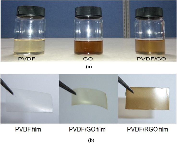
Figure 1. Images of (a) PVDF, GO and PVDF/GO hybrid gels and (b) their films.
Download figure:
Standard image High-resolution image2.3. Characterization techniques
The surface morphology and thickness of the GO nanosheets were investigated using a scanning probe (Multimode V, Veeco, USA) atomic force microscope (AFM). The chemical compositions of the films were studied by Fourier transform infrared spectroscopy (FTIR). FTIR was carried out on a FTS-2000 Scimitar spectrometer. The analysis of the phase transition was carried out by an x-ray diffractometer (D/Max B, Rigaku) with Cu Kα1 (λ = 1.540 56 Å) radiation. The surface morphology of the films was imaged with the help of a field emission scanning electron microscope (SEM: JEOL JSM 6500F) equipped with an energy-dispersive spectrometer (EDS) for compositional analysis. The dielectric permittivity and loss tangent were measured by a 4192A LF impedance analyzer from 10 Hz to 1 MHz. Hysteresis analysis was carried out using a Radiant Technologies precision premier ferroelectric testing device based on the modified Sawyer-tower technique. A magnetron sputtering system (KVS C4055) was used to deposit gold (40 nm) on the nanocomposite films as bottom and top contacts. A conventional cantilever beam was used to harvest the energy from the composite films. A function generator (SCO-01P), controller (LAS-200), amplifier (PA25E-CE), accelerometer (IEPE-8341) and vibrator (LDS-V201-M4) were used to produce the signal and control the vibration strength. An oscilloscope (LeCroy) was connected to the harvester in order to measure the generated output voltage with different frequencies, accelerations and load resistances.
3. Results and discussion
3.1. Characterization of the GO nanosheets
To confirm the exfoliation of the graphite oxide into individual graphene oxide nanosheets, GO powder dissolved in water was deposited on a Si substrate to carry out the AFM. AFM measurements in tapping mode were used to investigate the thickness and shape of the GO nanosheets, as shown in figure 2. The presence of irregularly shaped nanosheets with uniform thickness and different lateral dimensions can be clearly seen. As shown from the height profiles recorded at different locations, thickness variation between the rough Si surface and the graphene nanosheets was observed at ∼1.3 nm while the lateral dimensions ranged from ∼100 to ∼600 nm. One can conclude from the thickness that complete exfoliation of GO down to individual GO nanosheets was achieved. The thickness was slightly higher than that of pure graphene (∼1 nm) due to the presence of oxygen functional groups attached to both sides of the graphene nanosheets. We can see from the later sections that the in situ thermal reduction of the GO entirely reduced the presence of oxygen-containing functional groups.

Figure 2. AFM images taken in tapping mode and line profiles of the GO nanosheets.
Download figure:
Standard image High-resolution image3.2. Dispersion of GO in PVDF
To observe the morphology of GO and RGO, the GO solution was drop cast on SiO2/Si substrates. It was then hot pressed at 150 ° C for 2 h to achieve the RGO. Figures 3(a) and (b) show GO and RGO flakes on SiO2 at the microscale and the corresponding EDX element analysis. The EDS analysis indicated that the GO flakes were devoid of elements such as K, Mn and S, which are usually added to graphite powder during oxidation. The results of the EDX elemental analysis for C and O are listed in table 1. The C contents in the GO and RGO were 38.24% and 39.37%, respectively. However, the O content of RGO was significantly reduced to 3.3% from 23.31% in the GO. The mass ratio of C/O was 1.6 in GO and increased to 11.9 in RGO. The O content in RGO was 3.3%, indicating that some oxygen-containing functional groups were still present in the RGO sample. Figures 3(c)–(e) show the corresponding EDS analysis for PVDF, PVDF/GO and PVDF/RGO. Elemental analysis results for pure PVDF and its composites are listed in table 2. The C contents of the PVDF, PVDF/GO and PVDF/RGO were 57.13, 58.53, and 50.70%, respectively, whereas the O contents of the PVDF/GO and PVDF/RGO were 2.26 and 0.81%, respectively. RGO nanoflakes with broad wrinkles or folds indicated the presence of few layer reduced graphene oxide, as shown in figure 4(a).
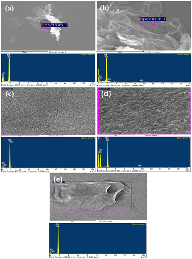
Figure 3. EDS analysis of (a) GO, (b) RGO, (c) PVDF, (d) PVDF/GO and (e) PVDF/RGO.
Download figure:
Standard image High-resolution imageTable 1. Result of the EDS elemental analysis for C and O.
| Element (wt%) | GO | RGO |
|---|---|---|
| C | 38.24 | 39.37 |
| O | 23.31 | 3.30 |
| Si | 38.45 | 57.33 |
| C/O ratio | 1.6 | 11.9 |
Table 2. Elemental analysis results for pure PVDF and its composites.
| Element | PVDF | PVDF/GO | PVDF/RGO |
|---|---|---|---|
| C | 57.13 | 58.53 | 50.70 |
| O | — | 2.26 | 0.81 |
| F | 12.91 | 8.06 | 7.67 |
| Si | 29.96 | 31.15 | 40.82 |
| C/O ratio | — | 25.89 | 62.5 |
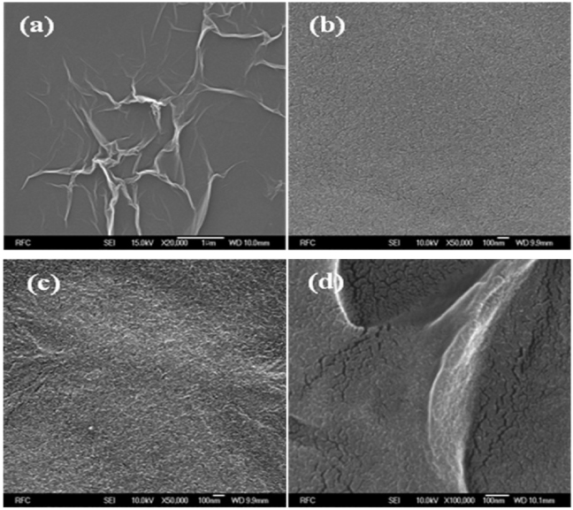
Figure 4. SEM images of (a) GO, (b) PVDF, (c) PVDF/GO and (d) PVDF/RGO.
Download figure:
Standard image High-resolution imageTo further study the original enhanced electrical properties of the nanocomposite films, the typical morphology of GO/RGO in the polymer matrix was analyzed. The typical FESEM image in figure 4(b) illustrates the morphology of pure PVDF. Figure 4(c) demonstrates that the GO nanosheets are well dispersed in the PVDF matrix, whereas figure 4(d) discloses a wrinkled topography of the PVDF/RGO nanocomposite film compared to the pure PVDF film.
3.3. Characterization of the nanocomposite films
The FTIR spectra of the drop-cast GO and thermally reduced GO on SiO2/Si are shown in figure 5(a). The oxygen-containing functional group of GO is represented in bands at 1419 and 1743 cm−1, corresponding to C–O–H deformation and C=O stretching of COOH groups, respectively. The peaks at 1635 cm−1 in GO and 1574 cm−1 in RGO represent the skeletal vibration of unoxidized graphitic domains. The broad absorption band at 3400 cm−1 indicates the presence of the O–H group in graphene oxide [28–31]. However, the oxygen-containing functional groups were almost entirely removed during the thermal reduction process. The peak at 3443 cm−1 in GO is absent in RGO due to the reduction process. Moreover, we cannot see the oxygen containing functional groups at 1419 cm−1 and 1743 cm−1 of GO in RGO. Hence, one can conclude that the absence of oxygen-containing functional groups in RGO may reduce the thickness of the GO (∼1.3 nm) to the thickness of pristine graphene (∼1 nm).
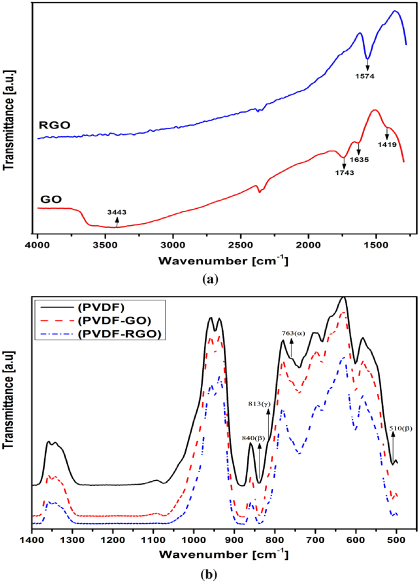
Figure 5. FTIR spectra of (a) GO and RGO, and (b) PVDF, PVDF/GO and PVDF/RGO.
Download figure:
Standard image High-resolution imagePVDF is known to have various crystalline phases based on the processing method, and alpha and gamma phases are predominantly obtained by the solution casting method. The beta phase in PVDF can be achieved by stretching and polling the film under a controlled environment. Knowledge of the microstructure changes of PVDF due to interaction with the various functional groups in GO and with the nanofillers of RGO is required to understand the mechanism of property enhancement.
Figure 5(b) depicts the FTIR spectroscopy results for the GO and RGO with PVDF. As shown, the PVDF made through our processing method yields a microstructure that is predominantly beta phase. The peaks at 510 cm−1 and 840 cm−1 represent the beta phase, whereas 763 cm−1 and 813 cm−1 represent the alpha and gamma phases, respectively. The beta and gamma phases produced in the microstructure are very similar. The dipole moment of DMF is mainly responsible for producing the gamma phase in PVDF [32]. In addition, the results confirm that the beta and gamma phases are not altered in the PVDF nanocomposites with the addition of GO and RGO. There is less alpha phase at 763 cm−1 in the PVDF/GO films due to the strong and specific interaction between the carbonyl group (>C = O) in the GO surface and fluorine groups (>CF2) in the PVDF. However, the peak almost disappears in PVDF/RGO due to the influence of conductive nanofillers offered by the partially reduced graphene oxide.
X-ray diffraction (XRD) measurements were carried out at 2θ angles from 5° to 30° to examine the crystalline phases in the solution cast films, as shown in figure 6. The peaks at 18.21° and 26.5° are attributed to the alpha phase and those at 20.22° belong to the beta phase. The addition of 0.1 wt% GO in PVDF reduced the prominent alpha phase. However, the peaks were not entirely removed as was reported by Achaby et al [27]. Although the beta phase was unaltered after reducing the GO, the alpha phase was slightly reduced relative to that of pure PVDF. This is possibly because RGO contains an insufficient amount of carbonyl groups to nucleate all PVDF chains into the required trans–trans (TT) conformation of beta phase. To obtain purely beta phase, the interaction between the carbonyl groups (>C = O) in RGO and the fluorine groups (>CF2) in PVDF can be enhanced by the inclusion of more GO and hence RGO. Although the RGO contains a very small amount of oxygen-containing functional groups, the EDS analysis indicated that still there was a presence of 0.81% of O content. Therefore, the inclusion of more RGO will increase the amount of carbonyl groups to nucleate all PVDF chains.

Figure 6. XRD spectra of PVDF, PVDF/GO and PVDF/RGO.
Download figure:
Standard image High-resolution image3.4. Electrical properties of the nanocomposite films
Figure 7 shows a comparison of dielectric permittivity and dielectric loss of pure PVDF and PVDF nanocomposites as a function of frequency at room temperature. PVDF/RGO, achieved by hot pressing at 150 ° C for 2 h, shows remarkable improvement in dielectric constant even at 0.1 wt% of GO. The dielectric constants of PVDF, PVDF/GO and PVDF/RGO are 16, 35 and 52, respectively, at 1 kHz. Although the dielectric constant is more than three times higher than that of PVDF at 1 kHz, the dielectric loss at 1 kHz is 1.12 for PVDF/RGO. The dielectric losses of PVDF and PVDF/GO are 0.5 and 0.64, respectively. The dielectric loss indicates that when the GO/PVDF nanocomposites are hot pressed, not all the functional groups in the GO are decomposed. We produced partially reduced graphene–PVDF nanocomposites. However, reduced graphene may not have the same properties as graphene. Thus, we achieved an increase in dielectric permittivity and dielectric loss, but not to the extent where the dielectric loss is greatly affected. Hot pressing of these films for a longer time may lead to complete decomposition of the functional groups in GO, which in turn may lead to high dielectric loss.
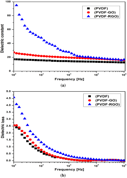
Figure 7. Comparison of (a) dielectric constant and (b) dielectric loss.
Download figure:
Standard image High-resolution imageThe improved dielectric constant of PVDF/RGO can be further explained by the microcapacitor model [33, 34]. Two neighboring RGO fillers can be regarded as electrodes in a local capacitor with a very thin PVDF layer as the dielectric. Each microcapacitor contributes an abnormally large capacitance, which can then be correlated with a significant increase in dielectric constant. The individual GO sheets are randomly distributed during the solution casting process. The graphene oxide sheets tend to align parallel to the film surface during solution flow and the solvent evaporation process due to the gravitational forces at the time of solution flow and the solvent evaporation process [35]. The alignment is further consolidated and partially reduced graphene oxide is formed due to the hot pressing.
3.5. Hysteresis testing
The effect of creating internal charge can be examined through hysteresis measurements. Figure 8 depicts the measured electrical polarization (P) of the samples versus applied electrical field (E), which is referred to as the PE hysteresis curve before and after poling. PE curves are necessary for validating a material's ferroelectric behavior at a particular temperature and frequency. The energy dissipation of the material produces a phase separation between the charge and voltage signals, giving a loop with a definable area under the curve. This area indicates the charge storage capability of the material. In an ideal ferroelectric polymer, we would expect that the charge accumulation would be due to the polarization of molecular dipoles. However, in a dielectric composite material, interfacial polarization occurs due to a swelling of charge at the inner dielectric boundaries of the conductively heterogeneous material [36]. In this situation, the nanoparticles are more conductive than the polymer, resulting in charge mobilization along the particles' perimeter, thus facilitating hetero polarization in the material [37]. Figure 8(a) represents the hysteresis loop without poling. The lower electrode of the film was gold whereas the upper electrode was platinum. The area of the upper electrode for all cases was 0.0254 cm2 and the thickness of the films was 50 μm. At a low electric field (50 kV cm−1), the remnant polarizations were 0.279, 0.316 and 0.434 μC cm−2 for pure PVDF, PVDF/GO and PVDF/RGO, respectively. The charge in PVDF/GO slightly increases from the pure PVDF due to the strong and specific interaction between the carbonyl groups (>C = O) on the GO surface and the fluorine groups (>CF2) in the PVDF. On the other hand, the remnant polarization in PVDF/RGO increases due to the hetero polarization.

Figure 8. Hysteresis loops: (a) before poling, (b) after poling.
Download figure:
Standard image High-resolution imageFilms with similar dimensions were subjected to corona poling under a high voltage of 12 kV at 60 ° C for 30 min. The electrodes were deposited in the same way. The hysteresis loop after poling is depicted in figure 8 (b). This time, the charge accumulation is increased due to the oriented molecular dipoles. Remnant polarizations of 0.89, 0.969 and 1.364 μC cm−2 were achieved for PVDF, PVDF/GO and PVDF/RGO, respectively.
3.6. Energy harvesting
The films were attached to a conventional cantilever beam to compare the energy harvesting capability of PVDF, PVDF/GO and PVDF/RGO. FR-4 material was used as the substrate. The length, width, and thickness of the cantilever beam were 25 mm, 10 mm and 400 μm respectively. The length, width and the thickness of the films were 14 mm, 10 mm and 50 μm respectively. The experimental setup for testing the proposed device is depicted in figure 9.

Figure 9. Experimental setup for energy harvesting.
Download figure:
Standard image High-resolution imageFigure 10(a) illustrates the peak–peak output voltages for PVDF, PVDF/GO and PVDF/RGO. PVDF/RGO shows clearly a higher voltage than those of the pure PVDF and PVDF/GO. The peak–peak voltages of PVDF/RGO, PVDF/GO and PVDF were around 1.3, 0.9 and 0.7 V respectively. Figure 10(b) depicts the comparison of Vrms voltage for different frequencies when the applied acceleration was 1g. The resonance frequency was 41 Hz. At this resonance frequency, the maximum Vrms voltages of PVDF/RGO, PVDF/GO and PVDF were 436, 312 and 288 mV respectively. The hysteresis loop indicates the charge storage capability of a material. The remnant polarization is directly proportional to the material's piezoelectric response [38]. As the remnant polarization of PVDF/RGO is higher than those of the PVDF/GO and PVDF, the output voltage is superior in the case of PVDF/RGO.
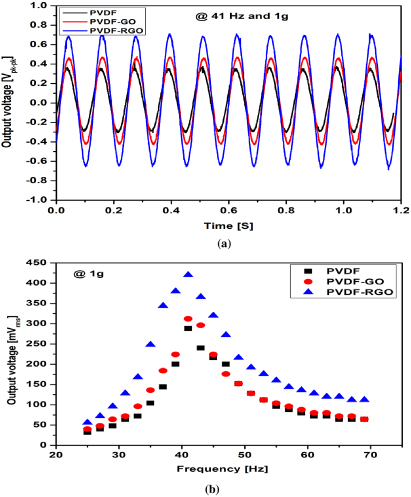
Figure 10. Output voltage: (a) waveforms, (b) comparison of output voltage with respect to the frequency.
Download figure:
Standard image High-resolution imageThe output voltage and power of PVDF/RGO with respect to various load resistances are shown in figure 11 for a resonance frequency of 41 Hz and an acceleration of 1g. The output voltage increased with the load resistance, and the output power of the harvester reached its maximum value at 704 kΩ. The harvester can generate a maximum power of 36 nW.

Figure 11. Output voltage and power for various load resistances.
Download figure:
Standard image High-resolution image
4. Conclusions
It was demonstrated that, through the addition of GO and in situ thermal reduction of the GO at a concentration of 0.1 wt%, the piezoelectric property can be enhanced to double that of pure PVDF. The property enhancement is due to the heterogeneous polarization offered by the conductive RGO nanofiller and the specific interaction between the PVDF chain and the partially reduced graphene oxide functional group. The remnant polarization of the PVDF/RGO was increased by 53.2% compared with pure PVDF. The output Vrms voltage of PVDF/GO (312 mV) was slightly higher than that of pure PVDF (288 mV), but it was 51.38% higher in the case of PVDF/RGO with respect to pure PVDF. The energy harvesting capability of PVDF/RGO showed better performance than the pure PVDF and PVDF/GO. These performance differences offer a new specific polymer-based material. Such novel piezoelectric partially reduced graphene nanocomposites could be of great value for future applications, ranging from broadband sensing to wearable energy scavenging.
Acknowledgments
Following are results of a study on the 'Leades INdustry-University Cooperation' Project, supported by the Ministry of Education, Science and Technology (MEST).