
Abstract
Conductive polymer composite, which can be used as the piezoresistive material of a flexible pressure sensor, has viscoelasticity. Therefore, the piezoresistivity is time dependent, introducing detrimental effects for sensor development. To reduce the time dependence, we designed a piezoresistive element with a novel structure called a 'nonalignment electrodes element (NAEE)', which is different from a traditional sandwich element (TSE). The experimental data under constant pressure show that the attenuation of the output resistance of a NAEE is much lower than that of a TSE, and the tend-to-stable-time (i.e. the shortest time needed to ensure that the output resistance of the element goes to a stable level) of a NAEE is far less than that of a TSE. The results verify the feasibility to reduce the time dependence substantially by using a NAEE.
Export citation and abstract BibTeX RIS
1. Introduction
Soft electronic elements are needed urgently in many modern industry fields [1–4], such as in fabricating flexible sensors and developing electronic skin. How to develop flexible pressure sensing elements has become a focus of attention. As external pressure can cause changes in the macroscopic electrical characteristics of functional materials (e.g. resistance, capacitance), pressure measurements can be realized through measuring these macroscopic electrical characteristics [5–11]. Therefore, many researchers have been engaged in developing flexible pressure sensors based on the piezocapacitive effect, piezoelectric effect, and piezoresistive effect. Recently, some researchers have fabricated flexible capacitive pressure sensing elements [12–16]. For example, Dobrzynska et al studied a polymer-based flexible capacitive sensor for three-axial force measurements [12]. Their results indicated that their transducer has great potential for use in skin-like sensing applications. Lei et al developed a flexible capacitive pressure sensor by using polydimethylsiloxane (PDMS) material as the dielectric layer because of its advantages of high dielectric constant and tunable elasticity [13]. Their sensor can measure pressures up to 945 kPa and is capable for most planar pressure measurements in biomechanical applications. Some other researchers have also used other membrane-based methods to develop flexible pressure elements [17–19]. For example, Chang et al used polyvinylidene fluoride (PVDF) and PDMS to develop a flexible piezoelectric sensor for microfluidic applications [18]. The flexible piezoelectric PVDF they fabricated can detect flow rates and impulse pressure signals. Apart from the aforementioned methods based on the piezocapacitive effect and the piezoelectric effect, the piezoresistive effect is a classic method to realize pressure measurements. The piezoresistive sensor can realize static pressure measurement, the method of the design circuit is mature, and the signal process system can be developed easily. Therefore, there is much research on piezoresistive sensors [20–24]. Conductive polymer composite is a popular material with flexibility and piezoresistivity [25–31]. Therefore, this kind of composite can be used to develop flexible piezoresistive elements [32–37]. However, this composite possesses viscoelasticity, leading to a time dependence of the piezoresistivity. Therefore, the electrical resistance of the composite changes with time under constant pressure [38, 39], which creates difficulties in developing a sensor. Many researchers have made great progress in studying the piezoresistive effects of the composites [40–43]. However, 'time' was seldom mentioned. Although there has been some research on the time dependence of the piezoresistivity of the composite [44–48], most only considered the time dependence from the viewpoint of mathematical analysis, without attempting to reduce it to facilitate the development of a sensor. Recently, some researchers have attempted to decrease the time dependence by adding nano-powders (e.g. nano-sized SiO2 fillers) into the polymer matrix [49, 50]. This method can reduce the time dependence to a certain extent. However, the reduction is not sufficient. Furthermore, adding nano-powders may lead to deterioration of the mechanical properties of the composite (e.g. flexibility). In this paper, we designed a piezoresistive element with a novel structure called a 'nonalignment electrodes element (NAEE)', the structure of which is different from that of the traditional sandwich element (TSE). The 'resistance creeps (the change in the resistance under a constant pressure is defined as "resistance creep" [38, 39])' of NAEEs and TSEs have been researched and compared. The experiment results show that the time dependence of the output resistance is reduced substantially by using NAEEs.
2. Experimental details
TSEs and NAEEs are composed of three layers (figure 1). The two outer layers are encapsulation films composed of insulating films (polyimide films) covered with copper electrodes. The medium layer is composed of the piezoresistive composite. Multi-walled carbon nanotubes were used as the conductive phase. They were obtained from Shenzhen Nanotech Port Co Ltd. They were made via chemical vapor deposition, with a purity of >95%. The average diameter and length are 50 nm and 10 μm. Room temperature vulcanized liquid silicone rubber (107#) is used as the insulating phase. It was obtained from Shenyang Silicone Plant. The dielectric constant and the dielectric strength are 3.0 and 15 kV mm−1. The mass ratio of carbon nanotubes to silicone rubber is 0.09. Hexane was used as solvent. After 6 h of vigorous mechanical mixing along with ultrasonic vibration, the solvent is evaporated. The viscous mixture is applied onto the surface of the encapsulation film. Then another encapsulation film is applied on top of the mixture. The entire structure is clamped between parallel plates during cross-linking. After the vulcanization, the two insulating films are adhered to each other. Pressure (0–0.5 MPa) is applied on the element by adding a force on the head (10 × 10 mm2). The electrical resistance was recorded by a digital multi-meter. The difference between the two elements is the configuration of the electrodes. For a TSE (figure 1(a)), the electrodes are vertically aligned. They are located in the pressure sensitive area. The sizes of the composite and the electrodes are 10 mm × 10 mm. For a NAEE (figures 1(b) and (c)), the electrodes are not aligned. They are situated outside the pressure sensitive area, and located on the different sides of the composite. The composite is a rectangular film (20 mm × 30 mm × 2 mm). The electrode is a rectangular sheet (5 mm × 5 mm × 0.3 mm). The distance between the centers of the electrodes is 25 mm. Figure 2 shows photos of the encapsulating films and a NAEE.
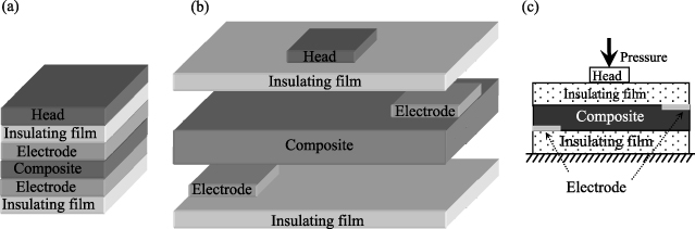
Figure 1. Schematics of a TSE and a NAEE. (a) Image of a TSE. (b) Image of a NAEE. (c) Cross-sectional view of a NAEE.
Download figure:
Standard image High-resolution image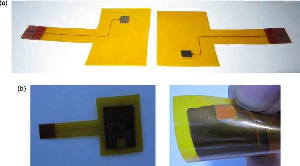
Figure 2. Photos of encapsulating films and a NAEE. (a) Insulating films and electrodes. (b) Picture of a NAEE.
Download figure:
Standard image High-resolution image3. Results and discussion
Figure 3 shows the five applied pressures and the outputs of a TSE and a NAEE. We can see that the resistances of the TSE and NAEE increase suddenly at the moment immediately after the pressure is applied, and then attenuate over time when the pressure is constant. To further study the resistance creep (the resistance attenuation under a constant pressure is defined as a resistance creep), the relative change in the resistance α of the element during the resistance creep is defined by:

where R(0−) is the resistance at the moment just before the compression, R(0+) is the resistance at the moment immediately after the compression, and R(60) is the resistance at the 60th second after the compression.
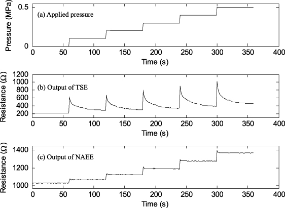
Figure 3. Applied pressures and outputs of a TSE and a NAEE.
Download figure:
Standard image High-resolution imageThe mean value of α for a NAEE is less than 21%, whereas that for a TSE is more than 89%. This indicates that the change in the resistance of a NAEE is far less than that of a TSE under constant pressure. The rate of change of the output signal of the element during the creep is defined as the average attenuation of the normalized resistance per second (the normalized resistance is the ratio of the resistance to the resistance at the initial moment of the creep). For practical implementation, the output signal of the element can be considered as stable when the rate of change of the normalized resistance is less than 0.001 s−1. The shortest time to ensure that the output resistance of the element reaches a stable level is called as the 'tend-to-stable-time'. The experimental data in figure 3 indicate that the average 'tend-to-stable-time' of a TSE is between 40 and 50 s, whereas that of a NAEE is between 3 and 4 s. We also use the traditional method (adding nano-powders into the composite) to fabricate sandwich elements with SiO2 (1–5 wt%) and test their resistance creeps. The results for the sandwich element with SiO2 indicate that the average 'tend-to-stable-time' is 15–25 s and α is around 45%. The aforementioned results show that the 'tend-to-stable-time' and α of a NAEE are not only much less than those of a TSE, but also far lower than those of the sandwich element with SiO2. Therefore, a NAEE can be used to reduce the time dependence effectively. As shown in figure 3, the sensitivity of a NAEE is lower than that of a TSE. The results indicate that the time dependence is reduced at the cost of some sensitivity. For applications without high demand for sensitivity, a NAEE can be used to reduce the time dependence.
Each test is repeated for 100 cycles. The results indicate that the element can withstand at least 100 measurement cycles. In the future, we will increase the number of the measurement cycles to determine the upper limit of the element. For the first ten measurement cycles, there are some deviations in the piezoresistivities, including the sensitivity, the reversibility, and the initial resistance at zero pressure. The sensitivity and the initial resistance at zero pressure degrade with an increasing number of measurement cycles, and there exist deviations from reversibility. However, the aforementioned deviations can be decreased by increasing the number of compression cycles. After the 10th measurement cycle, the variations in the sensitivity are very small, the deviation of the initial resistance at zero pressure is less than 0.5%, and the deviation from reversibility is also less than 0.5%. Therefore, in engineering applications, the problems (e.g. the variations in sensitivity, deviations from reversibility and the resistance under the zero pressure) can be overcome by applying several pre-compression cycles on the element. The experimental data in figure 3 are the test results in the 20th measurement cycle.
The temperature in the engineering application is around 25 ° C. Therefore, the aforementioned tests are done within this temperature range (24–26 ° C). The test results indicate that the deviation in the changes in piezoresistivity in this temperature range is less than 0.1%. In the future, we will widen the temperature range to study further the temperature sensitivity.
As shown in figure 2, the NAEE is now flexible. To study what happens if it is bent, we test the piezoresistivities of the element between the contacting surfaces with different radii of curvature (125, 150, 175, and 200 mm). The effects of bending on the output signal of the element are discussed as follows. The noise of the element is caused by the contact resistance between the composite and the electrodes. We use the method called 'vulcanization directly between electrodes' to fabricate the element. The composite is vulcanized directly between the electrodes. This method can reduce the contact resistance substantially. We have obtained a patent for this method [51]. Therefore, provided a good contact between the electrode and the composite is maintained, there is little noise when it is bent. Furthermore, the changing tendencies in the resistances of the element for different curvatures are similar to the results shown in figure 3. However, there exist deviations among the piezoresistivities of the same element with different curvatures (the maximum deviation is less than 10%). The sensitivity and the initial resistance also vary with the radius of curvature. The present results indicate that there are no definite relations between the radius of curvature and the sensitivity/initial resistance. The deviation in the initial resistance under zero pressure is less than 6%, and the deviation in the sensitivity is less than 5%. The aforementioned phenomena are caused by the different changes in the conductive networks of the composites under external pressure, which is induced by the different extent of curvature of the composite. Due to the existence of the aforementioned deviations among the piezoresistivities (sensitivity, initial resistance), using only one fitting curve to calibrate different elements will increase the measurement error. Therefore, the sensing elements should be calibrated separately for different radii of curvature. In many engineering applications, the sensor probes will not be moved after they are mounted when measuring the interlaminar pressure. Therefore, it is feasible to use the aforementioned calibration method before application.
Figures 4(a) and (b) show the schematics for the inner structures of a TSE and a NAEE. Each structure of the element is a three-dimensional network composed of carbon nanotubes and silicone rubber. The resistivity of silicone rubber is far higher than that of the carbon nanotubes. Therefore, the carbon nanotubes can be considered as electrodes, and the silicone rubber between the adjacent carbon nanotubes can be considered as the insulating film between the electrodes. According to the classic conclusions, we know that 'if two electrodes are separated by a thin insulating film, and the film is sufficiently thin, current can flow between the two electrodes by means of the tunnel effect' [52, 53]. Similarly, the tunneling effect occurs if the gap between the adjacent carbon nanotubes is small enough. Figure 4(c) shows the schematic of the tunneling effect in the composite. The silicone rubber film between the carbon nanotubes, where the tunneling effect occurs, is defined as 'tunneling film'. Based on the previous research [54–56], the resistance of the tunneling film can be calculated by:

where re is the value of the equivalent resistor of the tunneling film, D is the thickness of the tunneling film, φ is the height of potential barrier, c is the electron charge, m is the electron mass, h is Planck's constant, and S is the effective cross-sectional area of the tunneling film.

Figure 4. Schematics for the inner structures of a TSE and a NAEE. (a) Inner structure of a TSE. (b) Inner structure of a NAEE. (c) Schematic of the tunneling effect.
Download figure:
Standard image High-resolution imageUnder external pressure, the changes in the tunneling films and carbon nanotubes contribute to the variations in the electrical resistance of the composite. Therefore, the inner structure of the composite can be considered as a piezoresistive network composed of the tunneling films and carbon nanotubes. The piezoresistive network can be equivalent to a resistor network. Figure 5 shows the equivalent resistor networks of a TSE and a NAEE. Each equivalent resistor is composed of tunneling film and carbon nanotubes. Only the equivalent resistors located in the pressure sensitive area (the dotted line frame in figure 5(b)) can be changed by the pressure. They are defined as variable equivalent resistors (VERs). The equivalent resistors outside the sensitive area are defined as invariable equivalent resistors (IERs). Based on previous research on the piezoresistive effect of TSEs [42, 55, 56], the effective conductive path (ECP), which is composed of tunneling films and carbon nanotubes, can be considered as an elementary conductive unit of the composite. As shown in figure 5, each ECP connects the two electrodes. The changes in the ECPs lead to changes in the resistance of the element.
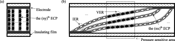
Figure 5. Equivalent resistor networks of a TSE and a NAEE. (a) Equivalent resistor network of a TSE. (b) Equivalent resistor network of a NAEE.
Download figure:
Standard image High-resolution imageAs shown in figure 5(a), there are Ny pieces of ECPs and Myny VERs in the (ny)th ECP in the equivalent resistor network of the TSE. Ny,ny and Myny are positive integers. The total resistance of the TSE Y can be calculated by:
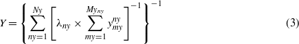
where  is the value of the resistance of the (my)th VER in the (ny)th ECP, λny is the (ny)th switch quantity for the (ny)th ECP of the TSE.
If λny equals 1, the corresponding ECP can contribute to the conductivity of the TSE. If λny equals 0, the corresponding ECP cannot contribute to the conductivity of the TSE, which is caused by the destruction of the ECPs in the TSE under the pressure.
As shown in figure 5(b), there are Nx pieces of ECPs in the resistor network of the NAEE. There are MXnx IERs and Mxnx VERs in the (nx)th ECP. Nx,nx,MXnx and Mxnx are positive integers. The total resistance of the NAEE X can be calculated by:
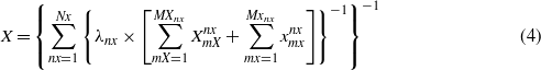
where  and
and  are the resistance of the (mX)th IER and the (mx)th VER in the (nx)th ECP, λnx is the (nx)th switch quantity for the (nx)th ECP of the NAEE.
If λnx equals 1, the corresponding ECP can contribute to the conductivity of the NAEE. If λnx equals 0, the corresponding ECP cannot contribute to the conductivity of the NAEE, which is caused by the destruction of ECPs in the NAEE under the pressure.
Based on the aforementioned analysis, there are two opposite changing trends of the resistance of the element under the pressure. Influence factors that contribute to an increasing trend of resistance are defined as 'positive factors', while influence factors that contribute to a decreasing trend are defined as 'negative factors'. Based on equations (2)–(4), the positive factors include the decrease in the number of ECPs caused by the destruction of the existing ECPs, the increase of the thickness of the tunneling film, and the decrease in the effective cross-sectional area of the tunneling film. The negative factors include the increase in the number of ECPs caused by the formation of new ECPs, the decrease in the thickness of the tunneling film, and the increase in the effective cross-sectional area of the tunneling film. For the convenience of discussion, the effect of the negative factors is called the destruction effect of the piezoresistive network, whereas the effect of the positive factors is called the formation effect of the piezoresistive network. The two opposite effects occur under pressure.
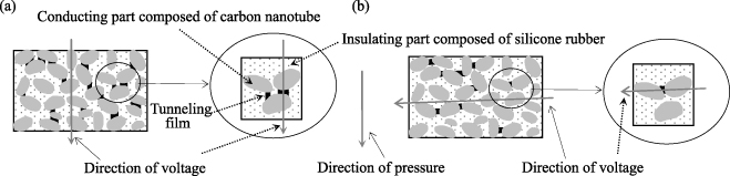
As shown in figure 3, the changes in the piezoresistive network can be divided into two stages. In the first stage (the element is loaded to a certain pressure), there is a sudden change in the piezoresistive network and the destruction effect is dominant. In the second stage (the element is under constant pressure after the load), the piezoresistive network continues to change and the formation effect is dominant. The reasons for the differences between the resistance creeps of NAEEs and TSEs are as follows. The different location of the electrodes leads to different directions for the voltage. The direction of the voltage for a TSE is parallel to the uniaxial direction of the element, whereas that for a NAEE is almost perpendicular to the uniaxial direction of the element. The different direction of voltage causes different directions of the current flowing the network, leading to a different shape of tunneling film (figures 6(a) and (b)). Therefore, although the morphology of the composite layer for NAEEs is the same as that for TSEs, the structure of the piezoresistive network for NAEEs is different from that for TSEs. Furthermore, the direction of the output signal of the piezoresistive network for TSEs is parallel to the direction of the pressure, whereas that for NAEEs is almost perpendicular to the direction of pressure (figures 6(a) and (b)). Moreover, the pressure sensitive area covers the whole piezoresistive network of TSEs (figure 4(a)), whereas the pressure sensitive area only covers the partial piezoresistive network of NAEEs (figure 4(b)). The aforementioned reasons contribute to the differences in the responses of the piezoresistive networks to pressure, leading to the difference between the resistance creep of NAEEs and that of TSEs.
Figure 6. Schematics for the piezoresistive networks of TSEs and NAEEs. (a) Local piezoresistive network of TSEs. (b) Local piezoresistive network of NAEEs.
Download figure:
Standard image High-resolution image
4. Conclusions
In conclusion, the resistance attenuation of NAEEs is far less than that of TSEs under constant pressure, and the tend-to-stable-time of NAEEs is also much lower than that of TSEs. The theoretical purpose of this work is to research the piezoresistive effect of conductive polymer composite with a new structure (NAEE). The application value is in verifying the feasibility of using NAEEs to reduce substantially the time dependence of the output of piezoresistive elements based on conductive polymer composite.
In the future, the key technologies of sensor systems based on NAEEs should be further studied, including improvements in the encapsulation of the sensor probe, the development of the signal processing system, among others. Furthermore, the piezoresistive mechanism of NAEEs should be further researched, e.g. the establishment of a precise model for the piezoresistivity of NAEEs. Moreover, the effects of other sensing factors (e.g. temperature sensitivity, fatigue life, dielectric constants, etc) should be further investigated.
Acknowledgments
This work was supported by 'Specialized Research Fund for the Doctoral Program of Higher Education' (No. 20100042120037), 'Shenyang's Science and Technology Plan Project' (F12-277-1-16, F10-205-1-63), and 'the Fundamental Research Funds for the Central Universities' (N110404028, N090404002).