
Abstract
We present high-speed force probes with on-chip actuation and sensing for the measurement of pN-scale forces at the microsecond timescale. We achieve a high resonant frequency in water (1–100 kHz) with requisite low spring constants (0.3–40 pN nm−1) and low integrated force noise (1–100 pN) by targeting probe dimensions on the order of 300 nm thick, 1–2 μm wide and 30–200 μm long. Forces are measured using silicon piezoresistors, while the probes are actuated thermally with an aluminum unimorph and silicon heater. The piezoresistive sensors are designed using the open-source numerical optimization code that incorporates constraints on operating temperature. Parylene passivation enables operation in ionic media and we demonstrate simultaneous actuation and sensing. The improved design and fabrication techniques that we describe enable a 10–20-fold improvement in force resolution or measurement bandwidth over prior piezoresistive cantilevers of comparable thickness.
Export citation and abstract BibTeX RIS
1. Introduction
A variety of instruments have been developed for the precise measurement of force and displacement over the past 25 years. The most commonly used techniques are atomic force microscopy, magnetic tweezers and optical tweezers [1]. These tools are capable of measuring force (10−14–10−8 N), displacement (10−10–10−4 m) and time (10−4–102 s) over many orders of magnitude [2]. However, none are capable of simultaneously measuring and delivering pN-scale forces with microsecond time resolution.
The ideal force probe should have comparable stiffness to the sample of interest (e.g. 0.1–10 pN nm−1 for cells and molecules) while maintaining a high resonant frequency during operation in liquid. Optical and magnetic tweezers can be built with vanishingly small spring constants (e.g. 10−3 pN nm−1) but their bandwidth is limited to 1–10 kHz by the mass of the bead and maximum trap spring constant. Atomic force microscopy cantilevers have been fabricated with resonant frequencies of several hundred kilohertz in water [3], but their spring constants have been correspondingly large (e.g. 200–300 pN nm−1) due to a minimum feature size set by the laser beam spot size.
We have addressed this technological gap with the development of force probes with integrated piezoresistive force readout and thermal actuation. A cantilever beam structure minimizes the probe mass while allowing simple spring constant adjustment via probe length. Piezoresistive sensing enables sub-micron cantilever dimensions [4] and simple integration with on-chip thermal actuation for sub-millisecond force delivery.
Microcantilevers with integrated sensing and actuation have been reported previously [5–8]. However, they were designed for high-speed scanning probe microscopy, so were relatively large (e.g. 100 μm wide × 3 μm thick) and optimized displacement resolution at the expense of force resolution. In contrast, our devices are optimized for single point force measurements and are one to two orders of magnitude smaller than prior integrated devices. In this paper we present the design, fabrication and performance characterization of high-bandwidth force probes with integrated piezoresistive sensing and thermal actuation.
2. Design
The force probe layout and dimensions are presented in figure 1. The probe consists of a narrow, soft sensor at the end of a wide, stiff actuator. Actuation is achieved by dissipating electrical power in a silicon heater in order to induce a temperature increase and thermal expansion in an overlaid Al film. We have designed and fabricated two different probe varieties: sensor-only devices and probes with integrated sensing and actuation. The sensor-only devices do not include an actuator but retain the stiffened base, which minimizes spring constant and resonant frequency variation between devices from the relatively imprecise backside release etch. We will show that placing the actuator at the base rather than the tip, in contrast with prior work [7], maximizes the tip deflection range, maximizes the overall resonant frequency of the probe, minimizes the thermal actuator time constant and decouples the mechanical design of the sensor and actuator portions. The fact that the sensor will have a much smaller spring constant and resonant frequency than the actuator allows the independent design and optimization of each portion of the force probe.

Figure 1. Layout of a force probe with integrated piezoresistive sensing and thermal actuation. The probe consists of a narrow, soft sensor attached to the end of a wide, stiff actuator. Placement of the actuator at the base rather than the tip leads to numerous performance benefits and decouples the mechanical and thermal designs of the actuator and sensor. Inset: power dissipation in the silicon heater induces a temperature increase and actuation through the expansion of the Al film. Heat is conducted along the length of the force probe and directly into the surrounding fluid.
Download figure:
Standard image2.1. Piezoresistive sensor
Force probes that are simultaneously soft and fast must be made as small as possible. While a zero-dimensional probe (i.e. a bead) minimizes the mass, its spring constant cannot be easily adjusted which limits the maximum measurement bandwidth. A one-dimensional probe (i.e. a cantilever beam) remedies this limitation by allowing bandwidth adjustment via the cantilever beam length. Any additional dimensions (e.g. tines for capacitive readout) simply contribute additional mass. Accordingly, we chose to use a cantilever beam geometry. Piezoresistive transduction allows the lateral probe dimensions to be limited only by the available fabrication technology [4].
The cantilever spring constant to resonant frequency in vacuum ratio scales as
where lc, wc and tc are the length, width and thickness of the cantilever, while Ec and ρc are its elastic modulus and density. We opted for a cantilever beam thickness of 300 nm because the reduction in thermal conductivity [9] and uncertainty in the effective elastic modulus [10, 11] of thinner probes lead to diminishing performance returns for piezoresistive cantilevers [12].
A thin cantilever beam requires a shallow piezoresistor. Sub-micron thick piezoresistive cantilevers have been fabricated using epitaxy [13, 14], ion implantation [15, 16] and diffusion [17]. For our application, diffusion yields higher performance than ion implantation and is far simpler than epitaxy while matching its performance. We chose to use POCl3 rather than BBr3 predeposition to avoid the formation of a boron-rich surface layer [18], to orient the piezoresistors in the 〈1 0 0〉 direction to minimize Ec and for the performance advantage of n-type piezoresistors for force sensing applications [19]. The piezoresistor is electrically isolated by a reverse-biased p–n junction and the substrate is grounded.
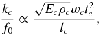
We have written extensively about piezoresistive cantilever design and optimization [19–22, 12]. The cantilever design is chosen to minimize the RMS force noise, equal to the minimum detectable force (MDF), in the intended measurement bandwidth. The MDF is calculated from

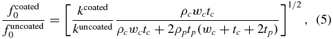
where VJ, VH, VA and VTMN are the integrated Johnson, 1/f, amplifier and thermomechanical voltage noise, respectively, while SFV is the voltage-referred force sensitivity of the piezoresistive sensor. Johnson and 1/f noise typically limit the resolution of optimized piezoresistive cantilevers, and the force resolution can be approximated as
where Tpr is the average piezoresistor temperature, Rpr is the piezoresistor resistance, fmin and fmax define the measurement bandwidth, Vb is the Wheatstone bridge bias voltage, α is the Hooge factor, Neff is the effective number of carriers and πmaxL is the maximum possible piezoresistive coefficient for the given dopant type and orientation [22]. The resistance factor (γ) is the ratio of the piezoresistor resistance to the total resistance including interconnects and contacts, while the sensitivity factor (β*) is calculated from the dopant concentration profile and accounts for both the finite depth of the piezoresistor and the decrease in piezoresistive coefficients with increasing dopant concentration [21].
The piezoresistive cantilever design, even before we account for self-heating and fluid damping, is clearly too complex for analytical design optimization. Instead, we design the force probe sensor using numerical optimization [19]. Although the piezoresistor design problem is not convex, seeding the numerical optimizer with several random initial guesses yields a globally optimal design. The optimization code that we have developed is open source and can handle ion-implanted, diffused and epitaxial piezoresistors. Ion-implanted piezoresistors are designed from a precompiled lookup table, while diffused piezoresistors are designed from an experimentally validated analytical model [23].
The cantilever designs are optimized to minimize the MDF for a given measurement bandwidth. The damped resonant frequency and quality factor in both air and water are calculated from the existing theory [24]. Amplifier and thermomechanical noise (TMN), which are neglected in (2), are included in the model. The amplifier noise characteristics play a large role in determining the optimal piezoresistor resistance. Second-order effects, such as the slight reduction in sensitivity due to the transverse current flow at the end of the piezoresistive loop, are also included in the numerical model and become increasingly important as the piezoresistor size decreases.
The code includes an experimentally validated thermal model in order to enable the temperature-constrained cantilever design [12]. The probes are designed to limit the maximum and tip temperature increases to approximately 5 and 1 K during operation in water to avoid damage to biological samples. The temperature-constrained piezoresistor design leads to a shorter piezoresistor than the more conventional power-constrained design approach [12]. An additional benefit of a shorter piezoresistor is a reduction in the static device curvature due to the high dopant concentration near the piezoresistor surface [25, 26]. One final benefit of modeling the cantilevers numerically is that the static deflection range due to intrinsic stress in the deposited films can be predicted using the Monte Carlo method.
We designed force sensors ranging from 30 to 200 μm long in order to span wide spring constant (0.3–40 pN nm−1), resonant frequency (20–400 kHz in air, 1–100 kHz in water) and force resolution (1–100 pN) ranges. We opted to fabricate the force probes using optical lithography, leading to a minimum feature size of 500 nm. The overall sensor width is constant along the entire probe length and split between the two piezoresistor legs. We opted to design and fabricate both 1 and 2 μm wide sensors, and several specific designs will be described later in this paper.
2.2. Thermal actuator
The actuator consists of a silicon heater underneath layers of SiO2 and Al (figure 1). The heater increases the temperature of the actuator, deflecting the probe tip due to the mismatch in thermal expansion coefficients between Si (2.6 ppm K−1) and Al (23 ppm K−1). The electrical power dissipated in the heater is transported to the base of the force probe and into the surrounding fluid via thermal conduction. The thermal actuator design is a tradeoff between tip deflection, operating temperature and heater time constant. For example, a longer actuator enables larger tip deflections for a given temperature but increases the heater time constant.
Tip deflection scales with the actuator curvature, which is linearly proportional to the moment generated by the actuator about its neutral axis and inversely proportional to its second moment of area. The actuator curvature is calculated from [27]
where zi, Ei, Ai and Ii are the distance from the bottom of the actuator to the layer midpoint, the elastic modulus, the cross-sectional area and the moment of inertia of layer i. The actuator is modeled as a cantilever beam with Si (i = 1), SiO2 (i = 2) and Al (i = 3) layers, while the sensor consists of a single layer of Si. The actuator curvature is integrated twice in order to obtain the force probe deflection. Although the curvature drops to zero beyond the end of the actuator, the sensor mechanically amplifies the actuator motion. The tip deflection is maximized for a given temperature increase by choosing the SiO2 and Al thicknesses to place the neutral axis at roughly the SiO2–Al interface.
The electrical power dissipated in the silicon heater needs to heat up the overlaid Al in order to actuate the device; however, the two layers are separated by SiO2. The oxide layer should be as thin as possible to maintain good thermal coupling between the two layers, while remaining thick enough to provide an etch stop when the Al is patterned during fabrication. We opted for a SiO2 thickness of 100 nm, yielding a thermal resistance between the silicon heater and Al that is roughly ten times smaller than the thermal resistance from the heater to the base of the force probe.
The optimal Al actuator thickness, based purely upon actuation efficiency, would be about 300 nm. However, there are several other design considerations. First, the resonant frequency and spring constant of the actuator should both be significantly greater than that of the sensor in order to mechanically decouple their operation. Second, the silicon heater should extend at least 20 μm from the base of the probe in order to reduce the sensitivity to backside etch tolerances. Third, additional room is required at the end of the actuator for the piezoresistor-interconnect contacts. Excess resistance degrades the piezoresistor resolution, and we opted for 20 μm long contacts to limit the contact resistance to approximately 10% of the piezoresistor resistance. We balanced these requirements by choosing an actuator length of 60 μm, heater length of 20 μm and a 1 μm thick Al film, yielding a tip deflection of 100–300 nm K−1 depending on the sensor length.
Similarly, the overall width of the actuator section (20 μm) and the width of the heater (12 μm) are chosen to provide room for 2 μm wide interconnects to the piezoresistor with 2 μm wide gaps. The overall resonant frequency of the force probe, which we calculated numerically using the Rayleigh–Ritz method [28] and checked via finite element analysis (FEA), improves as the width of the actuator increases, further rationale for the placement of the actuator at the base of the force probe.
The steady-state temperature over the thermal actuator is calculated from a finite-difference-based model [12], while its dynamic response is calculated using a lumped parameter model. In the lumped parameter model, there are two paths for heat flow from the silicon heater to the ambient. The first heat flow path is along the length of the force probe from the heater to the silicon die at its base (Rcond). The second heat flow path is directly from the actuator into the surrounding fluid (Rconv). The overall thermal resistance (Ra) is calculated from the parallel combination of the two resistances, which are calculated from
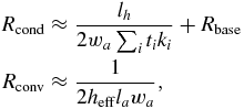
where wa and la are the overall dimensions of the actuator, lh is the length of the silicon heater, ti and ki are the thickness and thermal conductivity of each layer in the actuator and heff is the effective convection coefficient of the solid–fluid interface.
We include a non-zero thermal resistance (Rbase) between the base of the force probe and the large silicon die, which we previously showed was important in modeling cantilever self-heating [19]. The fixed thermal resistance is calculated as 1.4 and 1.1 K (mW)−1 in air and water, respectively, from a three-dimensional conduction–convection FEA model. We assume heff = 2000 and 50 000 W m−2 K−1 in air and water [19], while the thermal conductivities of the silicon and aluminum layers are taken as 100 and 200 W m−1 K−1, respectively [9, 29]. Radiated power is negligible because the devices operate near room temperature.
The heat capacity of the actuator is calculated over its entire volume as
where ρi and ci are the density and specific heat capacity of each layer in the actuator. Their values are taken from the literature [30].
The lumped parameter model is used to predict the actuator time constant (τ = RaCa), −3 dB frequency (f-3dB = 1/2πτ) and 10–90% rise time (tr ≈ 1/3f-3dB). The predicted time constant, −3 dB frequency and rise time in air are 13 μs, 13 kHz and 26 μs while in water they are 8.5 μs, 19 kHz and 17 μs, respectively. In comparison, the three-dimensional FEA model predicts rise times in air and water of 71 and 24 μs. The deviation between the lumped parameter and FEA models for air operation is due to the non-negligible thermal resistance between the heater and the distal end of the actuator. The additional time required for thermal transport to the end of the actuator results in a second, slower system response. The effect is smaller in water because more of the heat is conducted into the fluid before it reaches the end of the actuator.
Simulated actuator operation is presented in figure 2. The steady-state temperature profile of a force probe with a 61 μm long, 1 μm wide sensor and 60 μm long actuator operating in water is calculated using the finite-difference method and the model parameters that we have discussed. Joule heating in both the actuator and piezoresistor increase the temperature of the device. The simulated temperature profile is used to calculate the steady-state tip deflection (figure 2(b)).
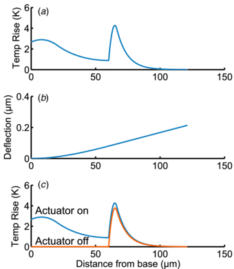
Figure 2. Thermal actuator operation. (a) Simulated steady-state temperature profile and (b) deflection along the length of a force probe with a 61 μm long, 1 μm wide sensor and 60 μm long actuator operating in water. The Wheatstone bridge bias and actuator voltage are both 1 V. (c) The average piezoresistor temperature increases approximately 250 mK for the simulated conditions when the actuator is turned on, leading to thermal crosstalk between the actuator and sensor.
Download figure:
Standard imageMechanical, thermal and capacitive crosstalk between the actuator and sensor present challenges for simultaneous actuation and sensing. For example, the average temperature of the piezoresistor increases approximately 250 mK during actuation (figure 2(c)), which is equivalent to approximately 90 times the piezoresistor noise floor. In order to compensate for actuator–sensor crosstalk, we fabricated all devices with two identical force probes and performed measurements differentially. Metal interconnects reduce both the excess interconnect resistance and mechanical crosstalk due to the lower gauge factor of Al compared with Si [6].
Mismatch between the dimensions and electrical properties of the main and compensation actuators can lead to differences in piezoresistor temperature if the same voltage is applied to both actuators. Later in this paper we will discuss a circuit-based compensation mechanism that uses a potentiometer to adjust the power dissipation in the compensation actuator to account for mismatch between the main and compensation force probes.
3. Fabrication
The seven-mask fabrication process is illustrated in figure 3. Force probes with and without integrated actuation are fabricated using the same process and identical film thicknesses. The process starts with a (1 0 0) oriented 100 mm diameter silicon-on-insulator (SOI) wafer with a 340 nm thick device layer, 400 nm thick buried oxide (BOX) and 400 μm thick handle wafer (Soitec). The device layer is p-type silicon with a resistivity of 10–20 Ω cm.

Figure 3. Fabrication process. (a) Alignment marks are patterned and etched. (b) The wafers are oxidized, coated with additional LTO and annealed. Windows are opened in the oxide mask and the contacts are POCl3 doped at 900 °C. (c) The oxide windows are opened further and the piezoresistors are POCl3 doped at 825 °C. (d) The oxide is stripped and the device layer is patterned and etched via RIE. (e) A layer of LTO is deposited and vias are opened. (f) The wafer is metallized and etched back via RIE. (g) An additional layer of LTO is deposited and cracks are patterned into the oxide stack. (h) The backside of the SOI wafer is patterned, a carrier wafer is bonded to the front side, the backside is etched via DRIE and the SOI wafer is debonded. (i) The BOX and LTO layers are etched via vapor HF in order to release the probes.
Download figure:
Standard imageAll lithography steps are performed using 0.7 μm thick SPR955 photoresist (unless otherwise noted) on an ASML PAS 5500/60 stepper with backside alignment capability. The critical dimensions and overlay tolerances of the device layouts are 0.5 and 0.25 μm, respectively. Small oxide vias (3–5 μm) are etched using buffered oxide etch (BOE) at several points in the process. In order to render the photoresist hydrophilic and ensure good etch uniformity, the wafers are exposed to 60 s of O2 plasma in a downstream asher prior to the wet etch.
Alignment marks are patterned and etched 120 nm into the device layer during the first step of the process. The wafer is rotated by 45° during the alignment mark exposure so that the piezoresistors will be oriented in the 〈1 0 0〉 direction ± 0.5° as set by the device layer orientation tolerance.
The oxide diffusion mask is formed next. A 90 nm thick thermal oxide layer is grown by oxidizing them in steam at 900 °C. The thermal oxidation decreases the thickness of the device layer from 340 to the target thickness of 300 nm. An additional 320 nm of low temperature oxide (LTO) is deposited on the wafers at 400 °C via low pressure chemical vapor deposition to increase the oxide thickness. The additional oxide is required to prevent phosphorus diffusion through the mask during the high temperature contact diffusion. Afterward the wafers are annealed in N2 at 1100 °C for 20 h in order to densify the LTO and reduce the residual strain gradient in the device layer. The thicknesses of the oxide films and silicon device layer are monitored throughout the process via variable angle spectroscopy ellipsometry.
The piezoresistive sensor is formed using two separate diffusions. First, the piezoresistor contacts are lithographically patterned and opened using BOE. The wafers are diffusion cleaned and the contacts are doped via POCl3 at 900 °C for 20 min. Afterward the wafers are dipped in 50:1 HF for 30 s to remove the thin surface layer of phosphosilicate glass (PSG) while leaving the underlying oxide mask intact. In the second diffusion, the window in the oxide diffusion mask is opened further using BOE to encompass both the contacts and piezoresistors. The earlier PSG removal reduces the undercut during this step. The piezoresistors are POCl3 doped at 825 °C for 30 min. Afterward the photoresist and remaining oxide are stripped.
The device layer is patterned and etched via Cl2/HBr reactive ion etching (RIE), with the Cl2:HBr ratio tuned to yield vertical sidewalls. Afterward the wafer is cleaned and 100 nm of LTO is deposited at 300 °C. The oxidation step at the start of the LTO deposition thins the device layer by 2–3 nm, yielding a 10–20% increase in the piezoresistor sheet resistance.
Oxide vias are lithographically patterned and etched in BOE, the wafers are diffusion cleaned and the native oxide is removed with a brief 50:1 HF dip before rapidly transferring the wafers to the sputterer load lock. In the load lock, the wafers are heated to 200 °C for 3 min via quartz lamps to drive off any moisture before 50 nm of Ti and 1000 nm of Al are sequentially deposited in the main process chamber. The Ti layer provides a lower barrier height than Al to n-type silicon and serves as a contact diffusion barrier [31–33].
The metal is lithographically patterned and etched back via Cl2/BCl3/N2 RIE, stopping on the underlying LTO layer. Afterward the wafers are rinsed in water to eliminate residual HCl on the wafer before the photoresist mask is stripped. Next a 400 nm thick LTO layer is deposited on the wafer and a trench is patterned and etched via CHF3/O2 RIE into the oxide around the force probe. The trench prevents cracks in the BOX from snapping the force probes, and increases probe yield from about 30% to 80% [34].
The backside of the wafer is patterned with a 7 μm thick layer of SPR220 and baked for 2 h at 90 °C to harden it. The front side of the wafer is left unprotected in order to maximize heat transfer during the backside deep reactive ion etch (DRIE). The wafers are shipped to the Lurie Nanofabrication Facility at the University of Michigan for the backside etch. The device wafers are bonded to a carrier wafer using CrystalBond 555 to facilitate the return shipment. A 25 mm diameter CrystalBond puddle is melted onto the carrier wafer at 110 °C, the front side of the device wafer is brought into contact with the carrier and vacuum is applied for 3–5 min. After the wafers are etched and shipped back, the backside photoresist is stripped and the carrier wafer is detached by immersion in 70 °C water for 30 min. The LTO coating deposited earlier prevents metal corrosion during this step. Afterward the wafer is cleaned in fresh DI water and air dried.
The wafers are cleaned in a downstream O2 plasma asher to remove residual DRIE passivation polymer. However, a thin layer of fluorocarbon polymer remains on the wafer because it is not volatile in pure O2 plasma [35]. Without further cleaning, a thin web of polymer remains on the wafer, rendering most of the devices unusable. A second polymer cleanup step is performed in a CF4/O2 plasma (100 mTorr, 9:1 O2:CF4) in order to remove the remaining fluorocarbon polymer. The silicon is protected from the plasma by the LTO encapsulation.
Finally, the BOX and LTO layers are etched in vapor HF in order to release the force probes. The wafers are etched from the front side, but cracks in the BOX allow the vapor HF to attack the BOX and LTO layers from both sides at once. The front side LTO thickness is chosen to match the BOX thickness in order to minimize undercut of either the LTO or BOX. Releasing the probes with pad etch led to stiction of the softest designs if a critical point drying step was not included, while backside RIE damaged the shallow piezoresistors. No forming gas anneal is used because it has a detrimental effect on the contact resistivity due to the shallow piezoresistors.
Scanning electron micrographs (SEMs) of finished sensor-only and sensor–actuator devices are presented in figure 4. After cleanroom fabrication is complete, the devices are snapped out of the wafer using snap tabs defined during the backside DRIE step. The devices are epoxied (5-Minute Epoxy, Devcon) to custom printed circuit boards (PCBs) and ultrasonically wirebonded with Al wire. Afterward the wirebonds are coated with epoxy and the entire assembly is coated with a 220–250 nm thick layer of parylene N (PDS 2010, Specialty Coating Systems). Passivation is required for operation in water to prevent corrosion and current leakage, but is not necessary for experiments in air or vacuum. The force probe PCB is connected to the readout circuit using a shielded RJ45 cable. Optical micrographs of a finished, assembled device are presented in figure 5. Two identical force probes are present on every silicon die for temperature and actuator crosstalk compensation, while a long extension enables compatibility with both upright and inverted microscopes.
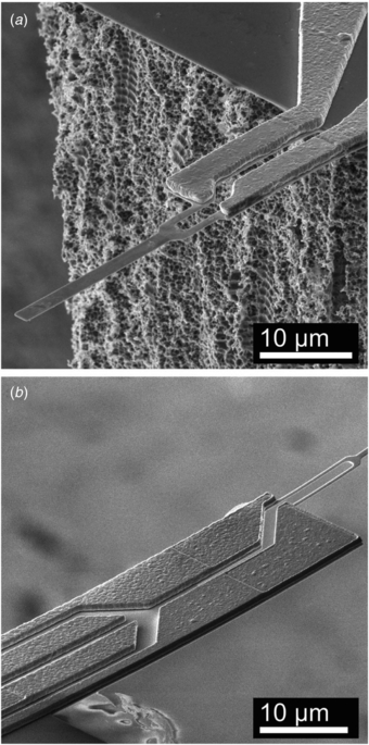
Figure 4. SEMs of completed force probes with (a) only piezoresistive sensing and (b) both piezoresistive sensing and integrated thermal actuation.
Download figure:
Standard image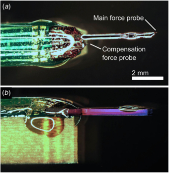
Figure 5. (a) Top and (b) side views of a fully assembled and passivated device. Two identical force probes are present on every silicon die. The main probe applies and senses mechanical forces, while the compensation probe cancels out common-mode resistance changes from simultaneous actuator and sensor operation or ambient temperature fluctuations.
Download figure:
Standard image4. Results and discussion
4.1. Force probe mechanics
We measured the resonant frequency, quality factor and spring constant of each sensor from its TMN [36]. The sensor tip deflection was transduced using a laser doppler vibrometer (LDV) with a 5 μm diameter laser beam spot size and measurement bandwidth of 800 kHz (Polytec OFV-2500). Noise spectra were averaged 200 times, recorded with a GPIB-controlled spectrum analyzer (HP 3562A) and converted from velocity to displacement noise spectra via the Laplace transform. TMN-based spring constant calibration is fast, non-contact, repeatable (to within about 5%) and does not depend on assuming any dimensions of the probe [37]. The resonant frequency (f0), quality factor (Q) and spring constant (kc) are calculated by numerically fitting a model to the measured spectra to minimize the squared sum of the relative residual error. The model includes the response of a thermally agitated simple harmonic oscillator and noise terms to account for the measurement system, and the displacement noise spectral density is calculated from
where kb is Boltzmann's constant, T is the ambient temperature, and A1, A2 and A3 are noise fitting parameters. The average cantilever temperature increase from the incident 1 mW, 633 nm laser is negligible (<10 K) because only a small fraction of the power (8%) is absorbed by the silicon. An example TMN spectrum is presented in figure 6. The measured TMN displacement spectral density is about 15 times the LDV noise floor (1 pm/ at 50 kHz) on resonance.
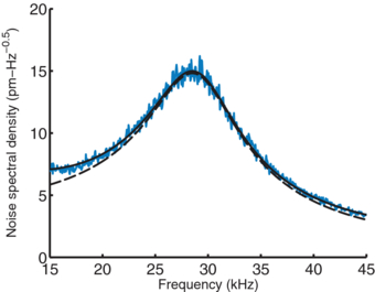
Figure 6. Example TMN spectrum for a 98 μm long and 2 μm wide force probe in air. The displacement noise spectral density of the probe is measured via LDV. The resonant frequency (f0 = 29.2 kHz), quality factor (Q = 3.3) and spring constant (kc = 1.4 pN nm−1) are extracted by numerically fitting a model (3) to the data (solid line) consisting of a simple harmonic oscillator at thermal equilibrium (dashed line) and noise terms.
Download figure:
Standard imageThe measured force probe resonant frequencies were slightly lower than expected (88 ± 8% of nominal, μ ± σ, N = 25), while their spring constants were slightly greater than expected (122 ± 28%). Both deviations are probably caused by residual oxide and sidewall stringers from the fabrication process. The results highlight the importance of calibrating small force probes with TMN rather than methods that depend on assumptions about the length, width or thickness of the devices.
The frequency responses of an example device in air and water are presented in figure 7. The model that we used to predict the resonant frequency and quality factor during the device design [24] matches the measured data to within 5% in both air and water based upon the nominal probe dimensions and fluid physical properties at room temperature.
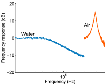
Figure 7. Frequency responses in air and water of a 35 μm long and 1 μm wide force probe. In air the resonant frequency and quality factor of the device are 290 kHz and 12.6 compared with predictions of 281 kHz and 12.8 from the model [24]. In water the resonant frequency and quality factor decrease to 85.2 kHz and 0.7 compared with model predictions of 84.3 kHz and 0.6.
Download figure:
Standard imageSurface passivation is required for operation in water due to corrosion of the Al interconnects and current leakage. The passivation layer should be as thin and soft as possible to minimize the impact on probe mechanics and force resolution. We utilized parylene N for surface passivation because it can be deposited in thin, conformal layers and has a relatively low elastic modulus. We previously demonstrated that parylene coating and water operation do not affect piezoresistor noise [19].
However, parylene passivation does affect the force probe mechanics. We measured the change in resonant frequency and spring constant of passivated probes over a range of parylene thicknesses (figure 8). The parylene thickness was measured via spectroscopic reflectometry and profilometry. The relative change in spring constant and undamped resonant frequency with passivation can be calculated from the standard multilayered linear elastic beam theory [27] as
where tp, Ep and ρp are the thickness, elastic modulus and density of the conformally deposited passivation coating. A schematic representation of a coated force probe is inset in figure 8. The best fit line (for 1 μm wide probes) corresponds to a parylene N elastic modulus of 5 GPa rather than the nominal 2.4 GPa. The stiffer than expected parylene may be due to the presence of a hardened surface layer observed by other researchers for similar deposition conditions [38]. We found that a coating of at least 230 nm is required to completely passivate the probes. Thinner coatings do not completely passivate the Al interconnects, potentially due to the undercut during the HF vapor release process.
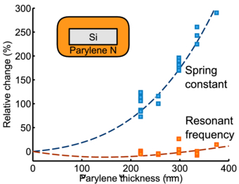
Figure 8. Experimental variation in spring constant and resonant frequency with parylene coating thickness. TMN spectra were recorded before and after parylene coating and the relative changes were calculated for matched pairs. The resonant frequency changes very little with coating, while the spring constant increases sharply. The best fit from (4) and (5) corresponds to an effective parylene elastic modulus of 5 GPa.
Download figure:
Standard imageAn additional issue with parylene coating is increased stiction of the softest force probe designs (< 3 pN nm−1). Soft uncoated devices often stick to the sidewall when removed from water but spring back to their initial shape. Parylene coated devices adhere more strongly to the sidewall and, if they come unstuck, often remain permanently bent due to plastic deformation of the parylene. We found that exchanging the water with a lower surface tension liquid (e.g. methanol) at the end of each experiment and applying heat until it completely evaporated eliminated this problem.
4.2. Piezoresistive sensor characterization
Each silicon die contains two identical force probes. The compensation probe, set far back from the tip of the device, provides both temperature and crosstalk compensation during simultaneous actuation and sensing. A Wheatstone bridge circuit transduces the resistance change of the piezoresistors into a voltage output. The silicon piezoresistors form the bottom two legs of the Wheatstone bridge while each side of the bridge is balanced with a wirewound potentiometer.
The Wheatstone bridge bias is generated by a 5 V voltage reference (ADR445), taken through a potentiometer-controlled voltage divider to set the desired bias and voltage buffered with an op–amp (AD8641). We found that a voltage reference yields comparable 60 Hz noise to a battery-powered circuit. The Wheatstone bridge output signal is amplified in two stages in order to maintain high bandwidth. First, a low noise instrumentation amplifier (INA103) amplifies the signal 100× (f-3dB = 800 kHz). A second-stage inverting op–amp (THS4031) provides further gain (1×, 10× or 100×) without degrading the system noise performance or measurement bandwidth. The frequency response of the entire signal conditioning path is calibrated by driving the instrumentation amplifier inputs with a 1 mV swept-frequency cosine (chirp) signal.
The electrical characteristics of the piezoresistive sensors are summarized in figure 9. The high dopant concentration at the surface of the contacts yields reliable ohmic contacts. The sheet resistance (110 Ω/□) and contact resistivity (10–20μΩ cm2) are measured from Van der Pauw and Kelvin Bridge test structures and match the measured resistances of the released force probes. The high contact doping minimizes both the contact resistivity and overall contact resistance, which is modeled as a one-dimensional ladder network. Overall, the contacts and metal interconnects contribute about 340 Ω of excess resistance, yielding resistance factors (γ) ranging from 0.83 to 0.96 depending on the piezoresistor length. In contrast, devices without the two-step diffusion and optimized metallization processes had excess resistances of 1–2 kΩ.
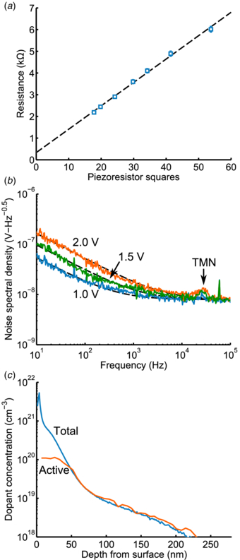
Figure 9. Summary of the piezoresistor electrical characteristics and noise performance. (a) The electrical resistance of released force probes with varying piezoresistor lengths. The contacts are ohmic and contribute 340 Ω of excess resistance. (b) The piezoresistors exhibit ideal 1/f noise and are capable of self-detecting their thermomechanical resonance in air (indicated). A noise model (1) is numerically fit to the spectra to calculate α based upon (c) the measured electrically active dopant concentration profile.
Download figure:
Standard imageExample piezoresistor noise spectra are presented in figure 9(b). The piezoresistor exhibits 1/f noise due to bulk mobility fluctuations. The Wheatstone bridge is biased to 1, 1.5 and 2 V and the power dissipation in the 2.8 kΩ piezoresistor ranges from 90 to 360 μW. When operated in air at these bias levels, the average piezoresistor temperature increase ranges from 7 to 30 K. The example device is capable of self-detecting its thermomechanical resonance in air (f0 = 30 kHz and Q = 3.6).
The Hooge factor, α, is calculated by numerically fitting the noise model, which includes Johnson, 1/f, amplifier and TMN, to the measured spectra. The simplified form of the noise model is presented in the numerator of (2). The electrically active dopant concentration profile is measured via spreading resistance analysis (Solecon Laboratories) and used to calculate the number of carriers in the piezoresistor (figure 9(c)). The total carrier concentration was measured via secondary ion mass spectrometry (Cameca NanoSIMS 50 L).
The spreading resistance measurements indicate a sensitivity factor (β*) of 0.23 ± 5% and an effective carrier density per unit area (Nz) of 4.13 × 10⁶ ± 23% (N = 3 for both measurements). The effective carrier density is about 20% smaller than the total carrier density due to variation in current density through the piezoresistor depth [39], and is calculated from
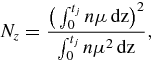
where z is the distance from the surface, n is the carrier density, μ is the carrier mobility [40] and tj is the junction depth. In this case, tj = tc because the piezoresistors are n-type doped throughout their thickness.
We measured α = 2.6 ± 1.4 × 10⁻⁵ (μ ± σ, N = 75), comparable with unannealed epitaxial boron piezoresistors [13], and confirmed that α was independent of piezoresistor length, width and bridge bias voltage. The Hooge factor is probably limited by interstitial phosphorus and the associated dislocations near the piezoresistor surface [41].
The piezoresistor displacement sensitivity is calibrated by applying a known deflection to the tip of the force probe. We mount the probe on a piezoelectric stage with capacitive position readout (Physik Instrumente P-517) and deflect the probe with a sub-micron ac deflection using a stationary, stiff AFM cantilever (42 N m−1, Nanoworld Arrow NCR). The experiment is performed underneath an upright microscope objective, with the probe placed on top of the AFM cantilever to avoid its sharp tip and to ensure that the contact point is within 1–2 μm of the force probe tip. Example calibration data are shown in figure 10. The measured and predicted displacement sensitivities match to within about 10%. Note that the displacement sensitivity (V m−1) is reported with respect to the Wheatstone bridge bias voltage (V (m−1 V)−1).
Figure 10. Example of displacement sensitivity calibration. The force probe is deflected 500 nm at 20 Hz and the output of the measurement circuit is recorded. The average displacement sensitivity for this 61 μm long and 1 μm wide force probe is 639 ± 17.9 V m−1 V−1 compared with a model prediction of 677 V m−1 V−1.
Download figure:
Standard imageThe force probe temperature during operation is monitored via the piezoresistor resistance. The resistance as a function of applied bias during operation in air and water is shown in figure 11. The corresponding temperature increase is calculated from the piezoresistor temperature coefficient of resistance (TCR). The TCR was calibrated as 1590 ± 150 ppm K−1 (μ ± σ, N = 5) using a temperature-controlled oven [12]. The change in piezoresistor temperature is used to validate the finite-difference-based thermal model (figure 11(b)) that we previously presented in [12] and to calculate the temperature along the entire length of the sensor during operation (figure 11(c)).
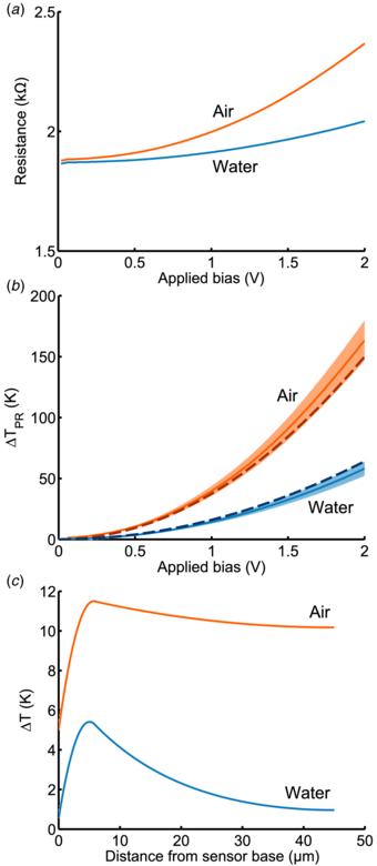
Figure 11. Force probe self-heating during operation. (a) The piezoresistor resistance of a parylene-coated force probe is measured as a function of the applied bias in air and water. (b) The corresponding temperature increase is calculated from the calibrated piezoresistor TCR. The average piezoresistor temperature predicted by a finite-difference-based thermal model [12] (dashed lines) matches the experimental data to within about 20%. (c) The validated model is used to predict the maximum and tip temperatures during operation at a 1 V bridge bias.
Download figure:
Standard imageFigure 12 compares the force resolution of the presented devices with prior single crystal silicon piezoresistive cantilevers operating in air [13, 17, 22, 42–45]. The cantilever dimensions, spring constant, resonant frequency, power dissipation and operating temperature vary significantly between devices. For example, the cantilevers that Harley reported in 1999 were 89 nm thick and operated with a maximum temperature increase of approximately 60 K in air compared with the present devices that are 300 nm thick and operate with a maximum temperature increase of less than 10 K. While piezoresistive cantilever operation in water has been reported previously, their integrated force noise was not stated [46, 47]. The performance of our devices has improved more than an order of magnitude over our earlier report of high-bandwidth piezoresistive force probes in 2009 due to both design optimization and fabrication improvements [45].
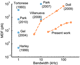
Figure 12. Force resolution comparison between this work and prior piezoresistive cantilevers operating in air. The fabrication and design advances described here enable a 10–20-fold improvement in force resolution or measurement bandwidth over prior devices of comparable thickness. The design and performance of the five devices from this work are described in more detail in table 1.
Download figure:
Standard imageThe design and performance of the five devices presented in figure 12 are described in more detail in table 1. The force and displacement resolutions are calculated for a 1 V bridge bias in order to limit the maximum and tip temperatures; resolution improves sub-linearly, while the temperature increases quadratically with the Wheatstone bridge bias. The piezoresistive sensors operate within a factor of 3–5 of the thermomechanical force noise floor in water.
Table 1. Summary of mechanical and sensor performance for selected devices operated at a Wheatstone bridge bias of 1 V. All of the probes are 300 nm thick and have a total width of 1 μm. Noise and resolution are calculated from 1 Hz to the resonant frequency of the sensor. Operation in water reduces the resonant frequency, quality factor and temperature increase from Joule heating, while the required parylene passivation layer increases the spring constant.
| Device number | 1 | 2 | 3 | 4 | 5 |
|---|---|---|---|---|---|
| lc (μm) | 96 | 75 | 61 | 46 | 35 |
| lpr (μm) | 9.5 | 7.7 | 6.6 | 5.2 | 4.1 |
| R (kΩ) | 5.16 | 3.97 | 3.94 | 3.15 | 2.65 |
| α × 10−5 (−) | 4.3 ± 1.3 | 3.0 ± 0.3 | 3.7 ± 1.5 | 2.7 ± 1.6 | 2.2 ± 1.7 |
| SXV (V m−1 V−1) | 352 ± 9.4 | 509 ± 29 | 639 ± 18 | 1160 ± 13 | 2080 ± 60 |
| Air operation (unpassivated) | |||||
| f0 (kHz) | 20.8 | 45.5 | 78.2 | 138 | 214 |
| Q (−) | 3.7 | 4.3 | 6.3 | 8.9 | 11.7 |
| kc (pN nm−1) | 1.12 ± 0.01 | 2.40 ± 0.21 | 4.72 ± 0.26 | 11.2 ± 0.97 | 20.8 ± 0.59 |
| ΔTmax/ΔTtip (K) | 7.2/1.5 | 7.6/2.5 | 7.9/3.6 | 8.4/5.2 | 8.9/6.6 |
| Vnoise (μV) | 2.49 | 2.83 | 3.40 | 3.76 | 4.06 |
| MDD (nm) | 7.1 ± 0.2 | 5.6 ± 0.3 | 5.3 ± 0.1 | 3.2 ± 0.0 | 2.0 ± 0.1 |
| MDF (pN) | 7.9 ± 0.2 | 13.3 ± 1.4 | 25.1 ± 1.5 | 36.2 ± 3.2 | 40.6 ± 1.7 |
| TMN floor (pN) | 0.9 | 1.2 | 1.4 | 1.8 | 2.2 |
| Water operation (220–250 nm of parylene N) | |||||
| fd (kHz) | 3.0 | 8.1 | 16.4 | 35.2 | 64.2 |
| Q (−) | 0.5 | 0.6 | 0.6 | 0.7 | 0.8 |
| kc (pN nm−1) | 2.32 ± 0.04 | 5.09 ± 0.37 | 9.91 ± 0.36 | 23.1 ± 0.76 | 43.4 ± 0.88 |
| ΔTmax/ΔTtip (K) | 3.0/0.0 | 3.4/0.0 | 3.6/0.0 | 3.9/0.0 | 4.1/0.2 |
| Vnoise (μV) | 1.83 | 1.90 | 2.29 | 2.49 | 2.74 |
| MDD (nm) | 5.2 ± 0.1 | 3.7 ± 0.2 | 3.6 ± 0.1 | 2.1 ± 0.1 | 1.3 ± 0.1 |
| MDF (pN) | 12.3 ± 0.8 | 18.8 ± 3.5 | 35.6 ± 2.9 | 50.4 ± 3.5 | 57.4 ± 3.6 |
| TMN floor (pN) | 3.5 | 4.7 | 6.6 | 9.3 | 12 |
4.3. Thermal actuator characterization
The frequency response of a force probe with a 61 μm long and 1 μm wide sensor combined with a 60 μm long actuator is presented in figure 13(a). For the measurements, the heater is dc biased (2 V) and then driven with a swept-frequency cosine (0.1 V). The dc bias provides a linear component to the actuation which simplifies the frequency response measurement. The transfer function is calculated from the power dissipation at the ac drive frequency. The measured dc actuator response of 560 nm mW−1 closely matches the 550 nm mW−1 (110 nm K−1) predicted from the finite-difference-based thermal model. However, the measured −3 dB bandwidth is 3.1 kHz compared with lumped parameter and FEA model predictions of 12.7 and 4.3 kHz, respectively. As noted earlier, the lumped parameter model overestimates the actuator bandwidth because it assumes negligible thermal resistance between the silicon heater and the rest of the actuator. For comparison, prior micromachined scanning probes with integrated thermal actuation have demonstrated −3 dB actuation bandwidths in air on the order of 300 Hz [48], 1 kHz [49] and 2 kHz [50].
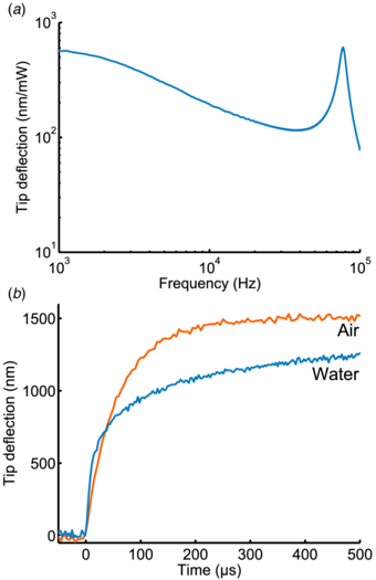
Figure 13. Thermal actuator frequency and step responses. (a) The frequency response in air has a significantly smaller bandwidth (3.1 kHz) compared with the lumped parameter model prediction (12.7 kHz). (b) The step response in air is characterized by a single time constant. In contrast, the step response in water has both fast and slow components due to heating of the surrounding liquid. The resulting 10–90% rise times in air and water are 92 and 80 μs, respectively.
Download figure:
Standard imageThe time-domain step responses of the same 61 μm long force probe design in air and water are presented in figure 13(b). The absolute deflection of the force probe tip was measured on an upright microscope by projecting the image of the tip onto a differential photodiode with a measurement bandwidth of 230 kHz. The heater power dissipation required for a given tip deflection is significantly greater in water (280 nm mW−1) than in air (560 nm mW−1) for a comparable tip deflection. Actuation in air is characterized by a single time constant (57 ± 1 μs). In contrast, the response in water is characterized by fast (10 ± 1.4 μs) and slow (108 ± 20 μs) components due to heating of the surrounding liquid. The 10–90% rise times in air and water are 92 ± 6.7 and 80 ± 4.9 μs. Actuation is about four times slower than the lumped parameter model predictions, indicating that variation in temperature throughout the actuator cannot be neglected.
Simultaneous actuation and sensing is demonstrated using the same force probe design (figure 14). The actuator is biased with a 1 V step (1.6 mW) filtered at 10 kHz with an eight-pole Bessel filter. The Wheatstone bridge is biased at 1 V, the signal is amplifier 1000-fold, filtered at 10 kHz and sampled at 100 ksps. The input referred crosstalk is on the order of 700 μVpp mW−1 if a board-level reference resistor is used to complete the Wheatstone bridge. The crosstalk decreases to 400 μVpp mW−1 if the resistor is swapped for an on-chip reference cantilever, but crosstalk is limited by electrical and thermal mismatch between the main and compensation actuators. Crosstalk decreases dramatically to 15 μVpp mW−1 if a resistor (50 Ω) and potentiometer are added in series with the thermal actuators (nominally 600 Ω) on the main and compensation probes, respectively. Adjustment of the potentiometer allows for fine tuning of the power dissipation in the compensation actuator to minimize any temperature mismatch between the main and compensation piezoresistors. The residual thermal crosstalk signal corresponds to a temperature mismatch of 40 mK mW−1 and has a time constant (50 ms) that is several orders of magnitude slower than the actuator time constant. The optimized crosstalk (15 μVpp mW−1) is equivalent to spurious deflection or force signals of 0.04 nm or 0.2 pN per nm of unloaded tip deflection.
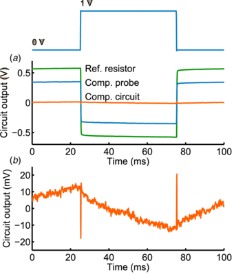
Figure 14. Simultaneous actuation and sensing. (a) Time-domain crosstalk between the thermal actuator and piezoresistive sensor for a 1 V (1.6 mW) step filtered at 10 kHz for three different crosstalk compensation strategies that use an off-chip reference resistor, on-chip compensation force probe, or the compensation probe combined with a resistive compensation circuit. (b) Detailed view of the fully compensated crosstalk performance. The residual input referred crosstalk is 15 μV mW−1 (40 mK mW−1). Capacitive coupling between the actuator and sensor is on the order of −90 dB at 10 kHz.
Download figure:
Standard imageOnce the thermal crosstalk is compensated, capacitive crosstalk becomes notable. The input referred capacitive crosstalk for an actuator step filtered at 10 kHz is −90 dB, smaller than the −70 dB [51] and −80 dB [6] results reported previously. Capacitive crosstalk is minimized through the combination of the compensation probe, metal rather than silicon interconnects to the piezoresistor, and the grounded, highly doped diffusion well that runs underneath the actuators for most of their length. However, improved capacitive crosstalk compensation will be necessary to take advantage of faster actuation methods [49].
5. Conclusions
We have presented high-speed force probes with on-chip actuation and sensing for the measurement of pN-scale forces at the microsecond timescale. We achieve a high resonant frequency in water (1–100 kHz) with requisite low spring constants (0.3–40 pN nm−1) and low integrated force noise (1–100 pN) by fabricating 300 nm thick, 1–2 μm wide and 30–200 μm long probes. We have demonstrated that the mechanical and electrical performance of the piezoresistive sensor matches the model predictions to within 10–20%. The improved design and fabrication techniques that we have described enable a 10–20-fold improvement in force resolution or measurement bandwidth over prior piezoresistive cantilevers of comparable thickness. We have also demonstrated thermal actuation in air and water with a bandwidth of 3 kHz and tip deflection of up to several microns. Thermal actuator speed could be increased in the future through decreased size, feedback control or input shaping. Finally, we demonstrated simultaneous thermal actuation and piezoresistive sensing with low thermal and capacitive crosstalk. We are currently using the force probes to study fast molecular and cellular mechanotransduction processes.
Acknowledgments
Fabrication work was performed at the Stanford and Lurie Nanofabrication Facilities (members of the NNIN) supported by the NSF under grant ECS-9731293. This work was supported by the Stanford Bio-X program, the NIH under grant EB006745, the NSF under CAREER Award ECS-0449400, COINS NSF-NSEC ECS-0425914 and CPN NSF-NSEC PHY-0425897, and by DARPA under YFA N66001-09-1-2089. Part of this research was conducted using a Cameca NanoSIMS 50 L, supported by the NSF under award no. 0922648. JCD was supported in part by NDSEG and NSF Graduate Research fellowships. The authors are grateful to A J Ricci and A W Peng (Stanford) for their helpful input on the probe design and for characterizing the actuator step response, and to S Martin and R Hower (U. Michigan) for their assistance with the backside DRIE.
: Appendix
The cantilever numerical modeling and optimization code is open source and freely available at http://microsystems.stanford.edu/piezoD. The code is written in object-oriented Matlab and requires at least Matlab R2008a with the optimization toolbox. Cantilevers based upon silicon piezoresistors (diffusion, epitaxy, ion implantation and polysilicon), metal strain gauges and piezoelectric films are supported in both end loaded and surface stress loaded configurations. The thermal and multilayered beam models are integrated into the code for both sensor and actuator designs.