

Abstract
An electrically pumped Sb-doped ZnO nanowire/Ga-doped ZnO p–n homojunction random laser is demonstrated. Catalyst-free Sb-doped ZnO nanowires were grown on a Ga-doped ZnO thin film on a Si substrate by chemical vapor deposition. The morphology of the as-grown titled nanowires was observed by scanning electron microscopy. X-ray photoelectron spectroscopy results indicated the incorporation of Sb dopants. Shallow acceptor states of Sb-doped nanowires were confirmed by photoluminescence measurements. Current–voltage measurements of ZnO nanowire structures assembled from p- and n-type materials showed a typical p–n diode characteristic with a threshold voltage of about 7.5 V. Very good photoresponse was observed in the UV region operated at 0 V and different reverse biases. Random lasing behavior with a low-threshold current of around 10 mA was demonstrated at room temperature. The output power was 170 nW at 30 mA.
Export citation and abstract BibTeX RIS
1. Introduction
Random lasers are gaining interest progressively for many promising applications, which include speckle-free projection, display and lighting, and medical diagnostics [1–3]. An essential requirement for strong random lasing is to achieve strong and recurrent scattering among the grain boundaries of a random medium for the formation of closed-loop feedback paths [4]. Zinc oxide (ZnO) is an excellent material for random lasing in the near-ultraviolet region, owing to its wide band gap (3.37 eV), large oscillator strength for high gain, and high refractive index for effective scattering [5]. Moreover, large exciton binding energy (60 meV) ensures abundant excitons at room temperature for low-threshold excitonic lasing by circumventing the population inversion requirement in regular electron–hole plasma lasing.
Current advancements in ZnO random lasing have been achieved from various low-dimensional structures such as nanocrystalline thin films [6], nanoribbon microcavities [7], nanowires [8], nanorods [9], and nanocombs [10]. While most of the reports demonstrate optically pumped random lasing in ZnO nanostructures [11, 12], electrically pumped ZnO-based random lasers with metal–insulator–semiconductor (MIS), heterojunction, and p–n junctions have also been reported [9, 13, 14]. However, there are very few reports on electrically pumped random lasers based on ZnO nanowires [9, 14–19]. Among all these types of devices, the p–n junction type remains desirable for high performance, but is still severely underdeveloped due to the issues of p-type doping. Sb, as one of the acceptor dopants for ZnO, has been demonstrated to produce p-type thin films [20] and nanowires [21]. Furthermore, homojunction LEDs [22], photodetectors [23], and Fabry–Perot (FP) diode lasers [24] have been reported. Nevertheless, no results on homojunction random laser devices based on Sb-doped p-type ZnO nanowires have been published. To realize the full potential of random lasing for the applications as outlined earlier, it is critical to further develop new devices aimed at higher performance such as lower threshold and higher optical power output compared with state-of-the-art devices. In this paper, the fabrication and characterization of a low-threshold Sb-doped ZnO nanowire/Ga-doped ZnO p–n homojunction random laser diode on Si is reported. With intentional growth of randomly distributed Sb-doped nanowires on n-type ZnO thin film, in contrast to strictly perpendicular ones, optical gain is obtained by light scattering among the nanowires to achieve random lasing rather than by constructive feedback inside the nanowires in the FP diode case [24].
2. Experimental details
Catalyst-free Sb-doped ZnO nanowires were grown by chemical vapor deposition (CVD) on high-quality Ga-doped ZnO thin film on an n-type Si (100) substrate. These Ga-doped ZnO thin films were grown using an SVTA radio frequency (RF) plasma-assisted molecular beam epitaxy (MBE) system. Effusion cells filled with elemental Zn (6N), Mg (6N), and Ga (6N) metals were used as Zn, Mg, and Ga sources. Zn, Mg, and Ga fluxes were controlled by the effusion cell temperatures. O2 (6N) gas was fed through the RF plasma generator as the oxygen source, and oxygen flow rate was precisely tuned by a mass flow controller. The Si substrates were cleaned using a standard RCA cleaning method. After being blown dry using a nitrogen gun, these substrates were immediately transferred to the MBE chamber. First, a thin MgO layer of ∼2 nm was grown on the Si substrate, followed by the growth of a ZnO buffer layer of about 10 nm at a substrate temperature of 450 °C. The Zn and Mg cell temperature was kept at 335 °C and 450 °C, respectively. The oxygen flow was 1.5 sccm and the RF power was 400 W. This MgO/ZnO bilayer helps improve the quality of the active ZnO film. Then, a Ga-doped n-type ZnO layer of about 500 nm was grown at a substrate temperature of 500 °C and a Zn and Ga effusion cell temperature of 340 °C and 565 °C respectively. The oxygen flow and RF power condition were kept the same as for the MgO/ZnO buffer growth. The growth time was 4 h. This thin film acts as both a seed for the subsequent growth of ZnO nanowires and an n-type component of the p–n junction laser device. Finally, the sample was taken out of the MBE chamber and transferred into a CVD tube furnace for ZnO nanowire growth. The ZnO film sample was positioned at the center of the furnace. A mixture of approximately 80% zinc and 20% Sb2O3 powder (volume ratio) in a glass bottle (O.D. × H = 15 mm × 45 mm) was placed ∼5 cm upstream of the sample. Both Zn and Sb2O3 were obtained from Sigma Aldrich and the purities were 99.999% and 99.99%, respectively. Under a constant flow of nitrogen gas (1000 sccm) for the whole growth period, the furnace was rapidly heated to 515 °C with a ramp rate of 30 °C min−1. A flow of the mixed argon/oxygen (molar ratio 99.5:0.5) gas of 320 sccm was introduced into the system after the substrate was heated to the desired temperature. The nanowire growth duration was 40 min, and then the furnace was cooled to room temperature. Part of the sample was covered by a piece of Si wafer during the growth for subsequent electrical contact deposition on the n-type ZnO film.
The structural properties of the nanowires were characterized by an XL30 scanning electron microscope (SEM). X-ray photoelectron spectroscopy (XPS) measurements were performed to determine the composition of the Sb-doped ZnO nanowires. XPS characterization was carried out using a Kratos AXIS ULTRADLD XPS system equipped with an Al Kα monochromated x-ray source and a 165 mm mean radius electron energy hemispherical analyzer. To estimate the acceptor activation energy of Sb-doped ZnO nanowires, temperature-dependent photoluminescence (PL) measurements were conducted. A He-Cd laser with an excitation wavelength of 325 nm and an excitation power of 5 mW was utilized in this experiment. To fabricate the ZnO homojunction diode, Ni–Au electrodes with thicknesses of 2 nm/5 nm were deposited on the p-type nanowires by the e-beam evaporation technique. On top of the Ni/Au contact, an indium tin oxide (ITO) glass slide (∼15–25 Ω sq−1) was used for reliable current feed through during electrical measurements. For the electrode of the n-type layer, Ti/Au (10 nm/100 nm) was deposited by e-beam evaporation. The device size was about 1 cm by 1.3 cm. Current–voltage (I–V) measurements were carried out using the combination of an Agilent 4155C Semiconductor Parameter Analyzer and a Signatone Probe Station (Model H150). Two probe arms of the station were used for this purpose. One of the arms was connected to the p-side of the device and supplied a variable voltage from −20 V to +20 V. The other arm held at 0 V served as the reference point and was connected to the n-side of the device. Photocurrent (PC) measurements were accomplished using a homebuilt system. The PC system includes an Oriel Xe arc lamp as the UV source. The light from the lamp travels through an Oriel 0.25 m monochromator and a specific wavelength light at its output port is produced. After chopping, the light is then radiated on the device. The generated PC signal is supplied to a lock-in amplifier from which the data are acquired. Electroluminescence (EL) of the device is collected in a similar way to PC measurement using another homebuilt system, which consists of an Oriel monochramator, a lock-in amplifer, and a chopper. The output power of the device was measured using a Thorlabs PM100 Optical Power Meter.
3. Results and discussion
Figures 1(a) and (b) show top-view and side-view SEM images of the nanowire array on the n-type Ga-doped ZnO seed layer, respectively. As seen from the images, most of the nanowires are randomly tilted by 20–25 degrees with respect to the normal of the substrate surface. The average length and diameter of these ZnO nanowires can be estimated as 1.5 μm and 110 nm, respectively. The size disparity of the nanowires may be attributed to the irregular grain sizes of the columnar ZnO seed layer. Typical hexagonal faceting of the ZnO nanowires is also evident from the images. The disordered nanowire morphology is generally beneficial for the random laser system since it increases the scattering of photons generated in the gain medium, thus increasing the dwell time or path length. As a result, light amplification is enhanced [25]. Figure 1(c) shows a representative XPS survey spectrum of the Sb-doped ZnO nanowires. Peaks relative to Zn, O, and Sb, together with a carbon peak can be observed in the spectrum. A carbon signal may originate from its exposure to air before the XPS measurements [26]. The O 1s peak overlaps with the Sb 3d5/2 and so quantification for this sample requires the use of a high-resolution spectrum over the Sb/O region (inset of figure 1(c)). As can be seen from the inset, the O 1s binding energy is 531.08 eV (indicated by the blue curve fit); the peaks located at 532.4 eV (indicated by the green curve fit) and 541.72 eV (indicated by the violet curve fit) correspond to the electronic state of Sb 3d5/2 and Sb 3d3/2, respectively, indicating that Sb has been incorporated into the ZnO nanowires. CasaXps was used to obtain the atomic concentrations of elements. The atomic concentration of Sb incorporated in the nanowires is 1.16%. The atomic concentrations for Zn and O are estimated to be 48.56% and 50.55%, respectively. Therefore, the stoichiometry of as-grown nanowires is oxygen rich with O:Zn = 1.04, which is important for successful p-type doping [27]. In addition, from the Sb 3d3/2 and Sb 3d5/2 peak positions, we can infer that Sb–O bonds exist, indicating that Sb atoms substitute Zn atoms (SbZn) [28]. The isolated SbZn is a donor in ZnO, which cannot result in p-type conductivity of the ZnO:Sb nanowires. It is supposed that a defect complex of Sb with two zinc vacancies (SbZn–2VZn) is the most possible shallow acceptor due to its low formation energy among all Sb-related complexes [29].
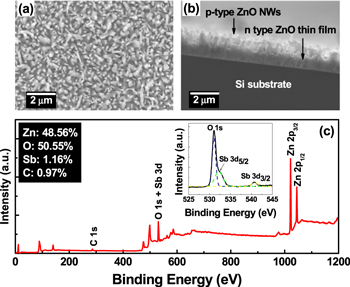
Figure 1. (a) Top-view and (b) side-view SEM images of Sb-doped ZnO nanowires grown on ZnO seed layer; (c) typical XPS survey spectrum for the ZnO:Sb nanowires. The inset shows a high-resolution XPS spectrum of the region between 525 and 545 eV.
Download figure:
Standard image High-resolution imageFigure 2 shows PL spectra of the sample. The near band edge (NBE) emission appears broad and flat, and consists of an acceptor-bound exciton (A°X) and neutral-donor-bound exciton (D°X) at 3.351 and 3.360 eV, respectively. This is reasonable since p-ZnO is a compensated semiconductor [30]. In addition, the PL signal may originate from both p-type nanowires and n-type ZnO thin film. Emissions at around 3.303 eV and 3.235 eV are identified as a free electron to acceptor (FA) transition and donor-acceptor-pair (DAP) transition, respectively [20]. The acceptor activation energy EA can be calculated with the equation [31, 32]

where the temperature-dependent transition EFA is approximately 3.296 eV at 13 K and the intrinsic band gap Egap = 3.436 eV at 13 K [33]. Therefore, the value of EA is calculated to be 0.13 eV, which is comparable to the previously reported value [20].
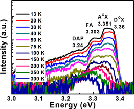
Figure 2. PL spectra of Sb-doped ZnO nanowires at different temperatures. The temperature ranges from 13 K to 300 K.
Download figure:
Standard image High-resolution imageFigure 3(a) shows the I–V curve of the device, showing a typical p–n diode characteristic with a good rectification ratio (about 33 at 10 V) and a threshold voltage of about 7.5 V. The result confirms the formation of an Sb-doped ZnO nanowire/Ga-doped ZnO thin film p–n homojunction. The inset of figure 3(a) shows a schematic of the electrically pumped lasing device. Figure 3(b) shows PC spectra at 0 V and different reverse biases. Very good response is observed in the UVA (400–320 nm) region. The PC signals are almost linear up to 366 nm, after which there is a sharp increase in the slope. The decrease of the PC with the decrease of light wavelength below 366 nm is associated with the change of the absorption coefficient. With increased incident photon energy, the light penetration depth is reduced due to higher absorption coefficient at shorter wavelengths. Therefore a smaller portion of the nanowires are excited. This accounts for the decrease in the yield of electron–hole pairs, and in turn, the decrease of the PC in this region. The peak around 380 nm (3.26 eV) corresponds to the effective band gap of ZnO. Under the illumination of the below-gap light, the PC signal starts to decrease before exhibiting a long 'tail' in the visible region. This PC tail is probably due to surface related defects [34]. As can be seen from figure 3(b), the PC increases with the increase of reverse bias. This is mostly because with increased reverse bias the thickness of the depletion layer of the junction increases, leading to more photon-generated electron–hole pairs contributing to the photocurrent. Therefore, it is solid proof of the formation of the p–n junction besides the I–V characteristics.
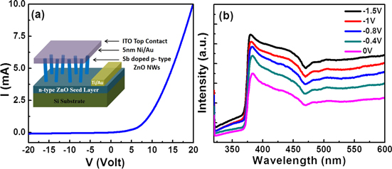
Figure 3. (a) I–V characteristic of the Sb-doped ZnO nanowire/Ga-doped ZnO film p–n homojunction device. The inset shows a schematic of the laser device; (b) PC spectra of the device under different reverse biases. The curves show good response in the UV region.
Download figure:
Standard image High-resolution imageFigure 4(a) shows EL spectra in 360–410 nm of the device, measured under different forward biases. The detector was placed directly in front of the emitting device. Under low injection currents of 5 mA and 7 mA, EL spontaneous emission in the UV region is observed and the intensity is so weak that it almost goes undetected. As the forward current is increased to 12 mA, the EL spectrum evolves into several discrete stimulated emission lasing modes. Further increase of the forward current to 30 mA leads to stronger lasing peaks as well as spontaneous emissions. The inset of figure 4(a) shows EL spectra measured at the same injection currents but with wider spectral range between 320 and 750 nm. It is evident that the lasing modes are centered in a region around 380 nm. No Zn plasma related emissions in the range of 320–335 nm and around 480 nm are observed even with 30 mA injection current at 38 V [15]. This is because the electric field across the p–n junction is reduced under the forward bias condition. Since carriers can freely move through those forward-biased nanowire junctions, no high electric field condition can be established to induce Zn plasma emissions [35]. Note that the spacing between the neighboring emission peaks and the peak positions between different measurements are not fixed. Therefore, the sharp emission peaks in the EL spectra should be related to the random lasing. Random lasers differ from conventional FP lasers in the way that the feedback is provided not by mirrors but by multiple scattering in disordered structures. Due to randomly tilted nanowire morphology and short nanowire length, conventional FP mode lasing could not be established in this device. Under forward bias, light is generated through excitonic recombination and is emitted in all directions. Some light propagating in the device is scattered multiple times by the nanowire sidewalls and thus trapped inside the structure. Because of high refractive index (n ≈ 2.3) ZnO nanowires lead to strong scattering. Some of the light can actually return to its initial position, and thus form a closed-loop resonant cavity [36]. The light is amplified and optical gain is enhanced in this resonant cavity. Lasing occurs as the optical gain is greater than the loss [37], where the gain is determined by how long the photons can dwell inside the structure and the loss refers to how easily light can escape to the surrounding air [38]. The full width at half maximum (FWHM) of these random lasing peaks at 30 mA is around 0.6 nm. Accordingly, we estimate a moderate quality (Q) factor of ∼650. This value is reasonable considering the morphology of the nanowires. As the nanowires are short (1.5 μm) and tilted, a fraction of light generated in the active region of the laser can escape to the surrounding air easily, leading to less effective reflections or scattering from the nanowire sidewalls. Thus, the quality of closed-loop random lasing cavities is compromised. Figure 4(b) shows spectrally integrated emission intensity as a function of current, which demonstrates a threshold current of ∼10 mA. The output power is 170 nW at a drive current of 30 mA. This output power is several times larger than that of a Schottky diode random laser [15], and orders of magnitude larger than that of a MIS-type device [9]. The inset of figure 4(b) shows a camera image of light emission from the surface of the lasing device at a drive current of 30 mA, which reveals strong violet luminescence at room temperature. The light emission pattern is different for different measurements, further indicating the random lasing nature.

Figure 4. (a) EL spectra of the laser device observed at different forward currents over the range from 5 mA to 30 mA at RT. Each spectrum is offset slightly on the y-axis for clear visualization. The inset shows EL spectra in an extended range from 320 nm to 750 nm; (b) the integrated intensity of the EL spectra versus drive current, indicating that the threshold current is about 10 mA. The inset shows a camera image of violet luminescence from this device at a drive current of 30 mA.
Download figure:
Standard image High-resolution image
4. Conclusion
Tilted, p-type Sb-doped ZnO nanowires have been prepared on an n-type ZnO seed layer. The formation of a p–n junction was confirmed by I–V and photocurrent characteristics. Random lasing centered around 380 nm was demonstrated at room temperature with a low-threshold current of 10 mA and significantly enhanced output power. The experimental demonstration of the homojunction random laser based on Sb-doped p-type ZnO nanowires paves a step for future practical applications of ZnO random lasers.
Acknowledgments
The authors acknowledge financial support from the Department of Energy (DE-FG02-08ER-46520).