

Abstract
Conventional nanoimprint lithography with expensive rigid molds is used to pattern ferroelectric polymer nanostructures on hard substrate for use in, e.g., organic electronics. The main innovation here is the use of inexpensive soft polycarbonate molds derived from recordable DVDs and reverse nanoimprint lithography at low pressure, which is compatible with flexible substrates. This approach was implemented to produce regular stripe arrays with a spacing of 700 nm from vinylidene fluoride co trifluoroethylene ferroelectric copolymer on flexible polyethylene terephthalate substrates. The nanostructures have very stable and switchable piezoelectric response and good crystallinity, and are highly promising for use in organic electronics enhanced or complemented by the unique properties of the ferroelectric polymer, such as bistable polarization, piezoelectric response, pyroelectric response, or electrocaloric function. The soft-mold reverse nanoimprint lithography also leaves little or no residual layer, affording good isolation of the nanostructures. This approach reduces the cost and facilitates large-area, high-throughput production of isolated functional polymer nanostructures on flexible substrates for the increasing application of ferroelectric polymers in flexible electronics.
Export citation and abstract BibTeX RIS
1. Introduction
Ferroelectric polymer nanostructures are of great interest due to their potential use in a wide range of applications, such as nonvolatile memories [1–3], organic electronics [4, 5], electric energy storage [6], and solid-state energy harvesting and conversion [7–10]. With the increasing interest in deploying ferroelectric polymers in flexible electronic technologies [11–14], fabrication of large-area, uniform ferroelectric polymer nanostructures with very good ferroelectric properties on flexible substrates will be an important basis for a wide range of research and applications. Previous studies of nanoimprinted ferroelectric polymers have used the conventional nanoimprinting technique with high-cost pretreated rigid molds pressing against polymer films at high pressure from 20 bar to 120 bar and raised temperature to produce ferroelectric nanostructures on hard substrates [1, 3, 15–19]. Conventional nanoimprint lithography done with flexible substrates can suffer from problems such as weak adhesion [20] and substrate deformation [21], which lead to low throughput and poor patterning quality [22, 23]. In addition, conventional nanoimprint lithography often requires an additional etching process to remove the residual polymer layer between the imprinted structures [24–26], and may not be compatible with flexible substrates, due to their poor etching resistance [27]. Previous research on reversal nanoimprinting, where the material is first coated onto rigid molds and then transferred onto the substrate, has fabricated amorphous poly(methyl methacrylate) (PMMA) structures on flexible substrates [28]. In order to produce large areas of useful nanostructures from functional polymers on flexible substrate, further studies of imprinting ferroelectric polymer nanostructures with flexible substrate and their crystalline structure and ferroelectric properties need to be explored.
Based on these considerations, we have developed a low-pressure reverse nanoimprint lithography method that uses low-cost polycarbonate soft molds to fabricate residual-layer-free ferroelectric polymer nanostructures over large areas on flexible substrates. The morphology and structure of the ferroelectric polymer nanostructures were characterized using scanning electron microscopy (SEM), atomic force microscopy (AFM), x-ray diffraction (XRD) and energy-dispersive x-ray spectroscopy (SEM-EDX). The ferroelectric property of the nanostructures was measured with piezoresponse force microscopy (PFM). The results showed that the nanostructures were faithful, high-yield replicas of the polycarbonate mold with no detectable residual layer and good crystallinity. The nanostructures also showed very stable and switchable ferroelectric polarization. The fabrication of large-area ferroelectric polymer nanostructures with very good ferroelectric properties on flexible substrates using the soft-mold-based low-pressure reverse nanoimprint lithography will be a significant basis for a wide range of research and applications for flexible electronics.
2. Experimental methods
The polycarbonate soft molds were prepared from recordable digital video disks (DVD-R, Verbatim). The DVD-R discs were cut in half to expose the cross-section, and the protective layer, together with the metal reflective layer, was gently peeled off. The organic phase-change medium filling the polycarbonate grooves was washed away with isopropanol, to produce clean and uniform line gratings with a period of 700 nm [29]. The discs were then cut into 2 cm × 2 cm wafers to serve as nanoimprint molds. The substrates, which consisted of 200 micron thick flexible polyethylene terephthalate (PET) coated with 40 nm of ITO (Sigma-Aldrich), were also cut into sizes of 2 cm by 2 cm and washed with dry acetone. To enhance the adhesion of the ferroelectric polymer to the PET substrates, they were modified by immersing them into a 0.1 M solution of (3-aminopropyl)triethoxysilane (APTES, Sigma Aldrich, used as received) in dry acetone at 60 °C for 10 min [1, 30].
The polycarbonate molds were coated with a P(VDF-TrFE) copolymer thin film using Langmuir–Blodgett (LB) deposition as follows. The copolymer P(VDF-TrFE) consisting of 70% vinylidene fluoride and 30% trifluoroethylene (Kunshan Hisense, used as received) was dissolved in dimethylsulfoxide to a concentration of 0.05% by weight. The thin film of 5 nominal monolayers (5 ML) was transferred to the mold surface by horizontal Langmuir–Blodgett (LB) deposition at a surface pressure of 5 mN m−1. The method of sample preparation and the properties of the film thus produced are described in greater detail elsewhere [31–33].
The reverse nanoimprint lithography experiments were carried out with a SPECAC laboratory hydraulic press system, as shown in figure 1(a). The polymer-coated polycarbonate mold was placed face-down on the ITO-coated PET and heated to 135 °C for 5 min. This temperature has been found to be optimum for promoting nanocrystalline self-assembly of P(VDF-TrFE) [34, 35]. A pressure of 6.8 bar was then applied to the mold for 1 h during which the pressure decreased to approximately 4.5 bar (see the supplemental information). The system was then cooled to room temperature within 90 min and the pressure was released and the sample separated from the mold.

Figure 1. (a) Reverse nanoimprint lithography procedure. (b) Photograph of a bent nanoimprinted sample made on flexible PET substrate. The sample has a rainbow color appearance in white light due to optical diffraction from the imprinted nanostructures. (c) SEM images of the P(VDF-TrFE) nanostructures on a bent PET substrate with a half cylinder sample mount.
Download figure:
Standard image High-resolution imageFor the scanning electron microscopy (SEM) measurement, a 2 cm × 2 cm nanoimprinted sample pre-coated with a 5 nm thick gold layer was bent and fixed tightly to the semi-circular face of a half cylinder sample mount with radius of 1 cm. Then, the surface morphologies of the P(VDF-TrFE) nanostructures were imaged by SEM (Hitachi model S4700 field-emission microscope) at an acceleration voltage of 15 kV.
The surface topographies of three test samples—a clean polycarbonate mold, a mold coated with a P(VDF-TrFE) LB film, and a imprinted nanostructure sample—were measured with an Asylum Research MFP-3D atomic force microscope (AFM) in tapping mode in a back-and-forth pattern that corresponds to the horizontal axis in all of the images.
The piezoresponse force microscopy (PFM) images of the out-of-plane piezoelectric response were carried out in contact mode using the high-voltage PFM module of the Asylum Research MFP-3D AFM and AC 240 TM cantilever made of a tetrahedral silicon tip coated with platinum/titanium (Mikromasch, CSC17/Pt) in a resonant-enhanced mode at a frequency of 170 kHz and a modulation amplitude of 0.8 V. The sample polarization was altered at specific locations with the tip in contact and applying a dc tip bias of up to ±12 V.
The crystalline structure of the imprinted nanostructures was studied by x-ray diffraction (XRD) using a Panalytical Empyrean x-ray diffractometer with the Cu-Kα emission line (1.54 Å). The sample was mounted on a spinning stage with speed of 0.25 rev/min. The out-of-plane (θ–2θ mode) diffraction signals were collected with 2θ ranging from 17° to 20° at step size of 0.013°. The XRD data was fitted to Lorentzian line shape function using Origin 9.0 [36].
The distribution of fluorine on the samples was imaged using the energy-dispersive x-ray spectroscopy (SEM-EDX) function of an FEI Nova NanoSEM 450 to test for the presence of a residual layer of P(VDF-TrFE) copolymer in between the nanoimprinted structures. The sample was pre-coated with a 10 nm carbon layer to reduce sample charging and the EDX mapping was performed in high vacuum with 5 kV acceleration voltage and optimized focus of approximately 10 nm in diameter. Mapping of fluorine distribution was acquired on a 2.4 μm × 2.4 μm region of the P(VDF-TrFE) nanostructures with 62 pixels in each horizontal line scan, equivalent to 38 nm intervals, and the total collection time was 300 s.
3. Results and discussion
The nanoimprinted sample had a uniform appearance over the substrate surface, as shown in the photograph in figure 1(b). The bent sample has a rainbow color appearance in white light due to optical diffraction from the imprinted nanostructures. The uniformity of the imprinted polymer stripes is clearly evident in the 40 μm by 30 μm SEM image shown in figure 1(c). Note that bending the PET substrate did not appear to damage or distort the morphology and uniformity of nanostructures.
To examine the reproduction quality of the reverse nanoimprint lithography process, we recorded high-resolution SEM images of the bare mold, the mold coated with ferroelectric copolymer, and the imprinted nanostructures. The images of the polycarbonate mold shown in figures 2(a)–(c) reveal a regular array of (nearly) straight parallel ridges with a period of 700 nm. The ridges on the polycarbonate mold were smooth and had very few defects. Figures 2(d)–(f) show the SEM images of the mold after coating with the copolymer LB film, showing that the LB film is highly conformal, coating the tops, sides, and bottoms of the DVD-R ridge pattern. The granular morphology seen most clearly in figure 2(f) is likely due to nanocrystals that form during deposition [37]. The copolymer-coated mold was pressed against the substrate at 135 °C and pressures up to 6.8 bar and then cooled to room temperature, as described above. When the mold and substrate were separated, the copolymer was found to have formed a negative replica of the mold on the PET substrate, as is shown in figures 2(g)–(i). Two observations can be made by inspecting the SEM images of the P(VDF-TrFE) nanostructures closely. First, although a maximum of only 6.8 bar was applied during imprinting, the resulting nanostructures were smooth and uniform over a large area. Second, the clean and smooth surface morphology between the nanostructures indicate that there was no apparent residual layer of P(VDF-TrFE) copolymer left between the ridges after imprinting.
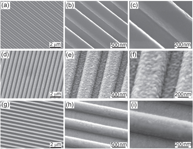
Figure 2. SEM images of three key stages in the reverse nanoimprint lithography. (a)–(c) The clean polycarbonate mold made from a DVD-R disk. (d)–(f) The same mold coated by LB deposition with 5 ML of P(VDF-TrFE) copolymer. (g)–(i) The nanostructures formed on a flexible PET substrate by the reverse nanoimprint lithography method.
Download figure:
Standard image High-resolution imageThe AFM topographies of the polycarbonate mold, the mold coated with copolymer, and the imprinted nanostructures are shown in figures 3(a)–(e). By comparing the AFM line scan results of the polymer-coated mold (red curve in figure 3(d)) with the original mold, we concluded that the copolymer coating was thinner on the sides of the mold ridges than at the tops and bottoms. The P(VDF-TrFE) nanostructures are uniform gratings with size of 160 nm ± 5 nm in height, an average of 330 ± 8 nm from the top and bottom widths and period of 715 ± 12 nm as measured from the AFM line scan result (red curve) in figure 3(e). In addition, the shape of the AFM profile line scan from the P(VDF-TrFE) nanostructures match very well with the AFM profile of the mold, shown by the blue shaded region in figure 3(e), which demonstrates that the shape of the imprinted copolymer is a precise negative replica of the mold. This means that during imprinting, the copolymer migrated into the mold valleys. In consideration of the results from both the SEM and the AFM images, we can conclude that during the reverse nanoimprint lithography process, an incomplete filling condition was reached [25], which effectively eliminated the residual layer in between the large area of uniform nanostructures. In addition, the use of a polycarbonate soft mold, which facilitates conformal and intimate contact of the mold with the substrate over large area even under low pressure, could be the reason why it works at such low pressure [38]. Without the benefit of the soft mold, ordinary nanoimprint lithography with rigid molds requires much higher pressure and tends to leave a residual layer up to 20% of the thickness of the nanostructures [3, 16, 18, 24–26].

Figure 3. (a) AFM topography of a clean mold. (b) AFM topography of a P(VDF-TrFE) coated mold. (c) AFM topography of the imprinted nanostructures. (d) Comparison between the AFM lateral line scan results of the clean mold and the P(VDF-TrFE) coated mold (red curve). (e) Comparison between the AFM lateral line scan results of the reversed clean mold (blue color region) and the imprinted P(VDF-TrFE) nanostructures (yellow color region), and the detailed dimensions of the P(VDF-TrFE) nanostructures.
Download figure:
Standard image High-resolution imageThe crystallinity and structure of the nanostructures imprinted on PET were characterized by out-of-plane x-ray diffraction. The XRD data (figure 4) were fit to a Lorentzian line-shape function consisting of a 17.9° ± 0.01° peak for the PET substrate from both samples and a second peak from the imprinted sample only at 19.55° ± 0.014° that comes from copolymer. This second peak is in excellent correspondence with previous XRD structural studies of well-annealed LB films of the ferroelectric copolymer, which have a peak at 2θ = 19.5°, corresponding to the (110) reflection from the ferroelectric β phase of the copolymer [39]. The XRD measurements, therefore, showed that the soft-mold-based low-pressure reverse nanoimprint lithography was able to prepare large-area ferroelectric phase P(VDF-TrFE) nanostructures with good crystallinity without any further annealing procedure.
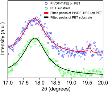
Figure 4. Out-of-plane XRD data from the imprinted P(VDF-TrFE) nanostructures (blue circles) and PET substrate (green circles) and the respective fits to Lorentzian-shaped diffraction peaks.
Download figure:
Standard image High-resolution imageIn order to investigate the functionality of the imprinted P(VDF-TrFE) nanostructures, the piezoelectric and ferroelectric properties were examined by piezoresponse force microscopy (PFM), which has been shown to be a powerful technique for characterizing piezoelectric and ferroelectric properties of material at the nanoscale [40–43]. The local PFM switching spectroscopy has been performed on the spots in the middle of the copolymer ridges (black dots in figure 5(a)) and in the middle of the valleys between the ridges (white dots in figure 5(a)). The hysteresis loops were obtained by holding the AFM tip at fixed locations (figure 5(a)), cycling the dc applied voltage in the ±12 V range, and recording the PFM phase and amplitude signals as a function of the dc bias. The difference between these two regions is striking: the piezoresponse amplitude loop on the copolymer ridges has a large, distinct butterfly shape (figure 5(b)), while the phase switches abruptly between opposing polarization states (figure 5(c)). The steep slopes in the phase near ±5 V and steady PFM amplitude after each switching cycle further confirmed that the copolymer ridges had highly stable, switchable polarization [44]. The hysteresis loops shown in figures 5(b)–(c) exhibit a slight horizontal shift of approximately 0.5 V toward positive voltage, which is likely due to the difference of the work functions between the Pt-coated PFM tip and the ITO bottom reference electrode. The larger PFM amplitude signal after poling at negative tip voltage compared to poling at positive tip voltage could be due to several conditions that are commonly encountered in PFM studies. The upward built-in electric field in the P(VDF-TrFE) nanostructure reduces the downward remnant polarization while increasing the upward remnant polarization, which will lead to a higher PFM signal at negative polings corresponding to the upward state [45–47]. The asymmetrical mechanical contact conditions between the platinum tip, polymer and ITO may also lead to asymmetry in the PFM signal when operating close to the tip-sample contact resonance frequency [48, 49]. The study of precise quantification of the PFM signal is still ongoing [49]. The non-symmetrical PFM amplitude signal in our current experiment is consistent with our previous measurement [50]. From the hysteresis loops, the coercive voltage of 5 V detected for the 160 nm thick P(VDF-TrFE) yields a coercive field of 30 MV m−1, which is approximately half the coercive field obtained with films of P(VDF-TrFE) made by spin coating [51], and three times the value obtained with ferroelectric nanopillars formed by direct nanoimprint lithography [1]. The valleys, in contrast, showed no evidence of polarization hysteresis, as shown in figures 5(d)–(e), suggesting that there is no residual ferroelectric layer there. This conclusion is consistent with the SEM and AFM morphology measurements showing no detectable polymer residual layer in the valleys between the P(VDF-TrFE) ridges.
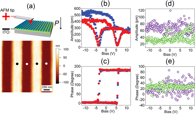
Figure 5. (a) AFM topography of the sample for the local PFM switching spectroscopy measurements and the experiment setup with AFM tip as top electrode and ITO as bottom electrode. (b) and (c) Amplitude and phase images of the PFM hysteresis loops measured on the imprinted nanostructure at the spots marked with black dots in (a). (d) and (e) Amplitude and phase images of the PFM hysteresis loops measured on the regions in between the imprinted nanostructure at the spots marked with white dots in (a).
Download figure:
Standard image High-resolution imageA local PFM polarization study was carried out on two spots on a randomly chosen strip, as is shown in figure 6. The PFM image recorded before voltage pulse application (figures 6(b)–(c)) showed that the polymer ridges were weakly polarized upward with several tiny domains of downward polarization. Then, the polymer ridge was poled at the two locations indicated by the red circles in figure 6(d) by positioning the AFM tip in contact with the polymer and applying a dc voltage of +10 V for 3 s. The PFM images (figures 6(e)–(f)) recorded after positive poling revealed the generation of downward polarized domains approximately 100 nm by 200 nm in size at the poling location. This is demonstrated by dark borders surrounding these regions in the amplitude image (figure 6(e)) and a bright contrast with 180° phase shift in the phase image (figure 6(f)). The same process was repeated with a dc voltage of −10 V applied for 3 s through the tip at the same locations (blue dots in figure 6(g)), followed by PFM imaging (figures 6(h)–(i)). The regions around the two poling spots reversed the polarization to be fully upward, with reversed phase and increased overall amplitude, compared to the weakly polarized initial state. Enhancement of the PFM amplitude signal after negative poling in figure 6(h) is an illustration of more complete poling of the P(VDF-TrFE) in comparison with its as-grown state [42].

Figure 6. (a)–(c) PFM topography, amplitude and phase image of the sample before applying voltage. (d)–(f) PFM topography, amplitude and phase images of the same area after applying +10 V for 3 s at the location of red dots with AFM tip as top electrode and ITO as bottom electrode. (g)–(i) PFM topography, amplitude and phase images of the same area after applying –10 V for 3 s at the location of blue dots with AFM tip as top electrode and ITO as bottom electrode.
Download figure:
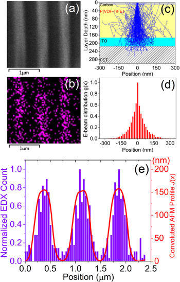
Standard image High-resolution imageTo further test for the presence of a residual layer of P(VDF-TrFE) copolymer in the valleys of the nanoimprinted structures, we mapped the distribution of fluorine using energy-dispersive x-ray spectroscopy (SEM-EDX). Since the PET substrate, ITO electrode and APTES surfactant do not contain fluorine, the SEM-EDX fluorine map should correspond only to the presence of the P(VDF-TrFE) copolymer. From the SEM image of figure 7(a) and the corresponding fluorine distribution in figure 7(b), we observe that the high fluorine counts are confined to the polymer ridges and therefore conclude that there is little or no residual layer of polymer between the ridges.
Figure 7. (a) and (b) SEM image and the corresponding EDX mapping of fluorine on the imprinted P(VDF-TrFE) nanostructures. (c) Monte Carlo simulation of the electron trajectories inside the three-layer model (200 electrons are displayed). (d) The accumulated histogram of the electron distribution g(x) with respect to horizontal position x. (e) Comparison of the accumulated EDX fluorine count from (b) with respect to lateral position x and the reference convoluted AFM profile J(x) of the P(VDF-TrFE) nanostructures.
Download figure:
Standard image High-resolution image
The EDX map, however, can only place an upper limit on the extent of the residual polymer layer. This is because the electron beam penetrates approximately 200 nm deep into the sample, well into the substrate, and thus limits the EDX resolution. To address the effect of the resolution limit on the EDX image, we performed a simulation of the sample as a three-layer model consist of 10 nm carbon, 160 nm P(VDF-TrFE) and 40 nm ITO, and used the Monte Carlo simulation software CASINO 2.4.8 [52] to calculate the electron scattering distribution within the sample. The simulation was performed using the Mott by interpolation for cross sections model to track 1000 electrons at 5 keV acceleration voltage over a 10 nm diameter focus on the sample. The simulated cross-sectional trajectories of the electrons inside the three-layer model are shown in figure 7(c), and the accumulated histogram of the electron distribution g(x) was calculated in figure 7(d) using Origin 9.0 software. The lateral profile (perpendicular to the polymer stripes) of the simulated EDX image was then calculated from the convolution  of the AFM topography h(x) of polymer nanostructures from figure 3(c) with the scattered electron distribution g(x). The convolution profile J(x), which represents the profile of the simulated EDX image assuming no residual layer, was used as the reference topography profile (red curve) in figure 3(e) for the quantitative analysis of the fluorine EDX mapping result. To quantify comparison of the model with the actual EDX image, we divided the accumulated EDX counts on the three P(VDF-TrFE) ridges (from figure 7(e)) by the signal collected from the regions in-between them and the calculated a contrast of 16.9 ± 2.7. This contrast coincided well with previous SEM-EDX studies of the interface between non-fluoro epoxy polymers and fluoropolymers, which showed a high contrast ratio of 12 to 15 between the signal collected from the fluoropolymer surface and non-fluoro epoxy polymer layer [53]. By scaling the amplitude of the EDX count distribution to the amplitude of the AFM profile, we calculate that the residual layer thickness is at most 160 nm/(16.9 ± 2.7) = 9.6 ± 1.6 nm. Previous research has shown that annealed P(VDF-TrFE) copolymer thin film from 5 nm to 10 nm showed very clear polarization hysteresis loops [31, 32, 54], which means that a residual layer this thick would be detectable by PFM. From the PFM studies shown in figure 5 no evidence of hysteresis loops were measured in regions in between the P(VDF-TrFE) ridges. By considering all the results from the SEM-EDX fluorine mapping along with the SEM, AFM, and PFM measurements we conclude that there is no detectable residual layer in between the P(VDF-TrFE) nanostructures.
4. Conclusions
We have developed a low-pressure reverse nanoimprint lithography method that uses low-cost polycarbonate soft molds to fabricate residual-layer-free ferroelectric polymer nanostructures over large areas on flexible substrates. The results of this study showed that the nanostructures were faithful, high-yield replicas of the polycarbonate mold with no detectable residual layer. The nanostructures have very stable and switchable piezoelectric response and good crystallinity, and are highly promising for use in organic electronics enhanced or complemented by the unique properties of the ferroelectric polymer, such as bistable polarization, piezoelectric response, pyroelectric response, or electrocaloric function. The soft-mold reverse nanoimprint lithography also works well with three-dimensional isolated structures, such as nanopillars, which will be reported separately. The fabrication of large-area ferroelectric polymer nanostructures with very good ferroelectric properties on flexible substrates using the soft-mold-based low-pressure reverse nanoimprint lithography will be a significant basis for a wide range of research and applications for flexible electronics.
Acknowledgments
We thank Prof Jiangyu Li and Prof. Barry Cheung for fruitful discussions, Prof You Zhou and Dr Xingzhong Li for assistance with SEM and EDX and Dr Shah Valloppilly and Yunlong Geng for assistance with the x-ray data analysis. This work was supported by the Department of Energy (DESC-0004530), the National Science Foundation (ECCS-1201384), a UNL Research Council Faculty Seed Grant Program, and by the National Science Foundation (NSF) through the Nebraska Materials Research Science and Engineering Center (MRSEC) under grant no. DMR-1420645 (PFM electrical characterization).
Supporting information
The supporting information describes the measurement of pressure used for the reverse nanoimprint lithography and the effect of the imprinting process on the morphology of the PET substrate.