Abstract
Organic photovoltaics (OPVs) fabricated via solution processing are an attractive way to realize low cost solar energy harvesting. Bulk heterojunction (BHJ) devices are the most successful design, but their morphology is less controllable. In this manuscript, we describe a simple approach to realize 'ordered' BHJ morphology using two immiscible solvents with different boiling point and a quasi-bilayer approach. Tunable fine structures were demonstrated in poly(3-hexylthiophene) (P3HT) and [6,6]-Phenyl C61 butyric acid methyl ester (PCBM) model systems, and the devices with optimized fine structure showed a 33% efficiency enhancement compared to those with a planar bilayer structure.
Export citation and abstract BibTeX RIS
Organic photovoltaics (OPVs) have been attracting significant interest as future power sources owing to the possibility of low-cost fabrication by solution processing and capability of obtaining flexible large area devices [1–3]. After the first report of two-layer OPV with ∼1% power conversion efficiency in 1986 by Tang et al [4], and the bulk heterojunction (BHJ) concept [1], immense efforts have been devoted toward obtaining high efficiency devices [5–12]. The efficiency of OPVs has been improved to over 10%. One of the breakthroughs in obtaining OPVs with enhanced efficiencies has been the introduction of the BHJ. BHJs can maximize the interfacial contact area between the donor and acceptor materials (thus allowing for efficienct carrier generation) and at the same time also provide efficient transport of electrons and holes in the devices. However, BHJs show several disadvantages—their blend morphologies are highly sensitive to the processing conditions because the nanoscale segregation of the donor and acceptor domains occurs via a non-equilibrium state during spinodal decomposition [13–15]. In addition, understanding the carrier transport in the mixed components is still speculative and is under study. On the other hand, the bilayer OPV device structure provides a good model system to study the charge transport properties and the interface between donor and acceptor. The bilayer structures show lower efficiency because the charge separation happens only at the interface of the two layers with different electron affinities. However, it has the advantage over BHJs from the point of view of charge transportation since the separated electrons and holes can be easily transported to each electrode with a lower possibility of recombination. Moreover, bilayer structures offer larger freedom to control the properties of the individual components and interfaces during device fabrication [16–19]. One way to overcome the lower efficiency in bilayer device is to increase the donor acceptor interfacial area in the bilayer structure through introducing of nanostructures in either donor (D) or acceptor (A) layers, which will reduce the distance between the acceptor and donor, allow for better charge transfer. Properly introducing nanostructure may lead to so-called ordered bulk heterojunction structure, which shows both large donor-acceptor interface area for exciton dissociation and good carrier transport due to more ordered donor and acceptor domains in the OPV device. Traditionally, imprint lithography techniques have been used to make a modified nano-pattern with templates such as microsphere colloidal arrays, porous anodic aluminum oxide, and silicon molds [20–27]. Although these techniques can modify the film easily, the processing is complicated and not suitable for scale-up. Hence, it is essential to simplify the processing to achieve large D/A contact area. In this paper, we introduce a simple effective technique to introduce micro-/nano-pore structures in organic film without any additional processes. By using immiscible solvents, we could fabricate well-organized nano/micro pore structures on the donor organic polymer layer.
In the process of using immiscible solvents for organic semiconductor device fabrication, it is essential to consider two important factors. One is the solubility of the organic semiconductors in the solvents, and the other is the vapor pressure of the solvents. In reality, it is challenging to gain a full understanding of the effects of the solvent on spin-coated polymer/fullerene blends. This is because many factors can affect the quality of the layer, including thermodynamic and kinetic parameters, the physical and chemical properties of each material etc However, from the dielectric constants, polarities, and dipole moments of solvents in addition to the presence or absence of hydrogen bonding, we can roughly estimate the solubility of organic compounds in a particular solvent. For example strongly polar compounds like sugars and salts dissolve well in polar solvents like water. Similarly, non-polar compounds like oils and waxes dissolve well in non-polar solvents like benzene and hexane.
High vapor pressure solvents like chloroform, ether, and acetone evaporate within few seconds at room temperature, while solvents with lower vapor pressure like water or glycol need much higher temperature and time. Previous studies have indicated that a mixture of solvents can change the morphology of the organic layer and improve the device performance [28–32]. By considering these two factors, we chose chloroform (CF) and ethylene glycol (EG) for our fabrication process. First these two solvents are immiscible with each other and quickly separate even when the mixture is shaken well. Additionally, CF by itself is a good solvent for poly(3-hexylthiophene) (P3HT), while EG does not dissolve P3HT.
This fast solvent separation process, however prohibits the fine micro-/nano-structure formation in the film during the solvent removal process. We solved this problem by adding small amounts of surfactant (e.g. commercial product DuPont™ Zonyl® FSO-100), through which we can make a temporary well mixed CF and EG emulsion, typically stable for one minute. As there is a large vapor pressure difference, EG exhibits a vapor pressure of 3.75 mm Hg, while CF exhibits value of 158 mm Hg, we expect that at room temperature, these two solvents exhibit significant differences in the solvent vaporization process. As the polymer P3HT can only be dissolved in CF, during spin-coating, CF will be easily evaporated, and then we can get a P3HT film with tiny EG domains which will then be evaporated and form micro- to nano-structures in the film.
There have been efforts using poly ethylene glycol (PEG) to form micro-structure in the polymer layer for OPV application [15]. However, PEG cannot be effectively removed from the active layer, which is not preferred for both OPV efficiency and long-term stability. EG on the other hand is much easier to remove than PEG.
Figure 1 shows a schematic of the fabrication sequence. First, we mixed CF and EG (figure 1(a)). As mentioned above, P3HT is highly soluble in CF but not EG These two solvents are immiscible and the mixture quickly separated, despite continuous stirring. Adding small amounts of surfactant (5 wt% vs EG) can allow EG to temporarily disperse into CF as a metastable emulsion. In device fabrication, (3,4-ethylenedioxythiophene)/poly(styrenesulfonate) (PEDOT:PSS, CLEVIOS P VP Al 4083) was first spin-coated on pre-cleaned indium tin oxide (ITO)/glass substrates at 4000 rpm for 30 sec (figure 1(b)). Then, the P3HT solution in (CF + EG) metastable mixture was spin-coated on top of PEDOT:PSS (figure 1(c)). During this step, the solvent with higher vapor pressure (i.e. CF) evaporated very quickly due to its low boiling point. However, a small amount of EG did not evaporate at room temperature and remained in the sample. Additional annealing of the film was then conducted at 150 °C for 5 min to remove EG Subsequently, a solution of [6,6]-Phenyl C61 butyric acid methyl ester (PCBM) in dichloromethane (DCM) was spin-coated on top of the P3HT layer (at 1000 rpm for 30 sec) (figure 1(d)). This solution-based casting of PCBM on top of the P3HT layer was facilitated by the limited solubility of P3HT in DCM. During the casting and thermal annealing of the PCBM layer, partial swelling and inter-diffusion of P3HT occurred. Hence, proximal to the contact area between the two materials, a concentration gradient of P3HT and PCBM could be created. This interpenetrating 'bilayer' structure with a concentration gradient can be expected to induce an increase in charge generation and separation, in addition to having an impact on the effective charge transportation and harvesting, similar to the active layer in BHJs structure [33–37]. In the final step, Ca/Al cathode was deposited to complete the device.
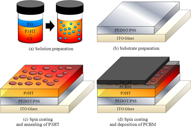
Figure 1. Schematic of the fabrication sequence of modified bumpy film in polymer solar cells using immiscible solvent. In the protocol, first (a) the solution was prepared. (b) Then, substrate with PEDOT:PSS was obtained. (c) In the next step, the P3HT+EG solution was spin coated and the product was annealed. (d) Finally, PCBM was spin-coated and metal deposition was carried out.
Download figure:
Standard image High-resolution imageSurface analysis was conducted by atomic force microscopy (AFM) and topographic images of the P3HT layers are shown in figure 2 (EG concentration (a) 0 wt%, (b) 0.5 wt%, (c) 1.0 wt%, and (d) 2.0 wt%, (e) 3D AFM of film from 1.0 wt% solution). The different topographies confirm the effectiveness of the process. At each different concentration of EG, the P3HT layer showed different peak to valley heights (Ra ) and root mean square (rms) roughness (Rq ). We observed that the sizes of the patterns are mainly dependent on the concentration of EG By adjusting the EG concentration in the range of 0–2 wt%, we obtained peak to valley heights of 3.7 nm (at 0 wt%), 5.9 nm (at 0.5 wt%), 37.7 nm (at 1.0 wt%), and 74.3 nm (at 2.0 wt%). More importantly, we were able to obtain micro-to nano-sized pores in the polymer films, which can serve as templates for D/A OPV cells much more ordered than a BHJ. For the 1.0 wt% EG case, the size of the holes is 200–500 nm. The roughness values—Ra and Rq , were 0.90 nm /1.15 nm (at 0 wt%), 0.10 nm/1.28 nm (at 0.5 wt%), 9.45 nm/11.9 nm (at 1.0 wt%), and 21.2 nm/28.1 nm (at 2.0 wt%), respectively. It is noted that high concentration EG resulted in excessively rough surfaces and significant shrinkage of the film during spin coating owing to a change in surface tension. We observed that over 3% EG concentration leads to very low yield of working device.
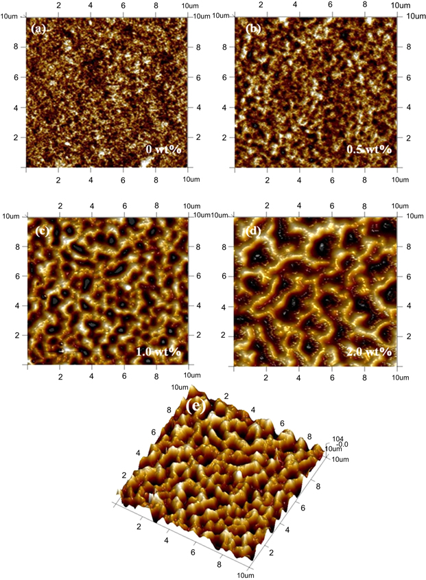
Figure 2. (a)–(d) Surface morphologies of P3HT films prepared from solutions with different EG concentrations (0–2 wt% vs CF) obtained by AFM. (e) 3D AFM image of film from P3HT solution with 1.0 wt% EG.
Download figure:
Standard image High-resolution imageTo further characterize the films, we also measured the optical absorption of (a) P3HT only films, (b) P3HT/PCBM films, and (c) P3HT/PCBM/Al films (reflective absorption) with different EG concentrations (0, 0.5, 1.0 and 2 wt%) in CF, and the results are shown in figure 3. Obtaining values with and without the reflective cathode gives information on the differences in the optical absorption due to light trapping or scattering of light reflected by the surface pattern. The reflective absorption also enables us to calculate internal quantum efficiency. We found that at higher concentrations of EG (i.e., with rougher structures), the cells showed lower absorption than common bilayer cells. This can be explained thusly, the volume of the pores increases with EG concentration and, as expected, this decreases the density of the P3HT layer and thus its—absorption. In our experimental approach, solution dilution is not critical because we only used up to 2 wt% of EG (i.e. CF:EG > 50:1 wt ratio). Therefore, it does not change solution viscosity much. As a result, the thickness of the film is virtually unchanged, which is confirmed by measurement using a Dektak 150 profilometer (measured thickness is 110 nm after PCBM spin coating). The difference in absorption is due to the different micro/nanopore size and distribution, rather than thickness variation. After PCBM was applied and annealed (figure 3(b)), we observed a relative absorption enhancement at the PCBM absorption wavelength, e.g. around 335 nm. We suspect the pores increase the capacity of the polymer layer to hold PCBM, thus the PCBM concentration in the layer increased. Finally, the devices were fabricated and measured under simulated AM 1.5G 1 sun irradiation using a Newport solar simulator. The device parameters—open circuit voltage (Voc), short circuit current density (Jsc), fill factor (FF), and PCE (η), were measured at room temperature. All the devices tested were annealed (at 150 °C for 10 min) before the deposition of Ca/Al. This annealing step is a well-known method to increase the performance of the P3HT/PCBM bilayer structure. Annealing will facilitate the inter-diffusion of PCBM and P3HT in the 'bilayer' architecture, further increase the D/A interface. Under identical fabrication conditions, we obtained a power conversion efficiency 3.43% with 1 wt% EG in the solvent. This corresponds to around 30% improvement in PCE when compared to the reference device with a planar bilayer structure (2.58% PCE). Jsc was significantly improved from 6.83 to 10.2 mA cm−2, and no change observed in Voc. The achieved Jsc is now very close to that in bulk heterojunction P3HT:PCBM solar cell devices [11]. Further details of the device performances are shown in table 1.
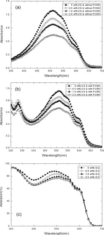
Figure 3. Absorption spectra acquired from (a) P3HT only film, (b) P3HT/PCBM film, and (c) reflective absorption of P3HT/PCBM/Al film from solutions containing different concentrations (wt%) of EG in the CF main solution.
Download figure:
Standard image High-resolution imageTable 1. Best device performances and error bar of the bilayer OPVs with different concentration of EG (wt%). The average efficiencies with error bar for each EG concentration are shown in the graph below.
| EG [wt%] | Voc [V] | Jsc [mA cm−2] | PCE [%] | FF [%] | Error [%] |
|---|---|---|---|---|---|
| 0 | 0.633 | 6.83 | 2.58 | 59.52 | 8.4 |
| 0.5 | 0.614 | 7.22 | 2.64 | 59.50 | 14.9 |
| 1 | 0.639 | 10.17 | 3.43 | 52.72 | 14.1 |
| 2 | 0.626 | 9.31 | 2.82 | 48.37 | 19.1 |
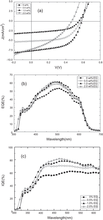
The average efficiencies with error bar (derived from typically 8–12 devices under each condition) are shown in the graph next to table 1. We observed that the rougher the P3HT film, the larger the variation. Never the less, we can clearly see that the device performance improved when 1.0 wt% EG was added to the solution, through which larger D/A area has been achieved. All the devices showed similar Voc values (of around 0.63 V), which indicates that the energy gap between the HOMO of the donor and the LUMO of the acceptor were not changed. Chabinyc et al [38] showed that under typical thermal annealing conditions (e.g. 150–175 °C 30 min) in bilayer P3HT/PCBM devices, there is a clear drive towards a homogeneous mixture of P3HT/PCBM from the initial heterogeneous state. Russell et al [34] showed evidence that in the bilayer structure, P3HT first crystallizes after a short time of thermal annealing. Longer annealing time leads to significant PCBM diffusion into the P3HT film via P3HT's amorphous domains. In our experiment design, introducing the micro/nano-sized pores in the P3HT film can significantly increase the P3HT:PCBM interface area over the planar interface. The micro/nanopore effect and the following annealing driven PCBM diffusion into P3HT is expected to form improved P3HT/PCBM nano-morphology, which is in between a BHJ and an annealed bilayer OPV devices. Very importantly, the P3HT crystallinity is well preserved in the whole process, and the formed morphology can both maintain a large donor/acceptor interface for charge generation, and also an interpenetrating donor & acceptor network to enable effective carrier transport.
We further measured the external quantum efficiency (EQE) as shown in figure 4. We can very clearly see the differences between devices made with EG added and those without. For example, devices without EG had lower EQE than the ones with it, especially in the wavelength range of 400–600 nm. This leads to the improvement in short circuit current density. It is interesting to note that the EQE is enhanced significantly even though the total absorption was smaller in the EG fabricated device. The IQE was also calculated based on the reflection absorption data. (Figure 4(c) The peak IQE of EG device was almost 40% higher than the reference device without it. The significant enhancement of internal quantum efficiency clearly shows the benefit of micro/nanopore formation for device morphology over planar bilayer devices, as the annealing conditions are the same. The improved morphology in turn leads to improvement of charge dissociation and transport and thus improved IQE.
Figure 4. (a) Current density–voltage (J–V) characteristics, (b) EQE, and (C) IQE of cells containing spin-coated layers with different EG concentrations.
Download figure:
Standard image High-resolution image
In summary, we successfully fabricated micro/nanoporous poly(3-hexylthiophene) polymer layers and the structures increased the interfacial area between the acceptor and donor. This technique allows for adjusting the sizes of the devices by changing the high boiling point solvent EG concentration. The controlled nanopore structure and following annealing driven PCBM diffusion into polymer domains enables formation of preferred D/A morphology, which led to improvements in the performance of the devices relative to the quasi-bilayer structure. The approach is expected to be general and provides a useful tool for improving OPV device performance in many polymer and solution processable small molecule solar cell systems.
Experimental section
Materials
Poly(3-hexylthiophene) (P3HT) was purchased from Rieke Metals, Inc. [6,6]-phenyl C 61-butyric acid methyl ester (PC61BM) was purchased from Nano-C. Poly(3,4-ethylenedioxythiophene)/poly(styrenesulfonate) (PEDOT:PSS, CLEVIOS P VP Al 4083) was purchased from H. C. Starck. All materials were used as received.
Device fabrication
The device structure is shown in figure 1. The solar cells were fabricated on ITO-coated glass substrates, with sheet resistance of 15 Ω/□. The organic solvent pre-cleaned ITO substrates were treated with UV-ozone. PEDOT:PSS was spin coated on ITO surface under 4000 rpm for 30 s, and then active layer with P3HT, PC60BM was spin-casted one by one at the same condition 4000 rpm for 30 s. After being baked at 150 C for 10 min, the substrates were transferred in to a thermal evaporator.
Measurement
The current density-voltage(I-V) curves were measured by using Keithley 2400 source meter under a simulated AM1.5G spectrum with an Oriel 9600 solar simulator at 0.8 Sun. External quantum efficiencies were measured using a lock-in amplifier (SR830, Stanford Research Systems) with a current preamplifier (SR570, Stanford Research Systems) under short-circuit conditions. Atomic force microscopy (AFM) images were taken on a Veeco digital instruments multimode scanning probe microscope. The absorption spectra were recorded using a Hitachi ultraviolet-visible U-4100 spectrophotometer (Hitachi High-Technologies Corporation, Tokyo, Japan).
Acknowledgments
This work was supported by the Postdoctoral Research Program of Sungkyunkwan University, Korea (2012). This work was also financially supported by Office of Naval Research (Grant no. N00014-11-1-0250; program manager: P Armistead), and National Science Foundation (Grant no. DMR-1210893; program manager: Andrew J Lovinger). G.L would like to thank the UCLA Henry Samueli School of Engineering and Applied Science for financial support. The authors thank Prof. Yang Yang and Dr Ziruo Hong for valuable technical discussions.