
Abstract
In this paper, we have performed a detailed investigation of the temperature- and current-dependent emission characteristics of nanowire light-emitting diodes, wherein InGaN/GaN dot-in-a-wire nanoscale heterostructures and a p-doped AlGaN electron blocking layer are incorporated in the device's active region to achieve white-light emission and to prevent electron overflow, respectively. Through these studies, the Auger coefficient is estimated to be in the range of ∼10−34 cm6 s−1 or less, which is nearly four orders of magnitude smaller than the commonly reported values of planar InGaN/GaN heterostructures, suggesting Auger recombination plays an essentially negligible role in the performance of GaN-based nanowire light-emitting diodes. It is observed, however, that the performance of such nanowire LEDs suffers severely from Shockley–Read–Hall recombination, which can account for nearly 40% of the total carrier recombination under moderate injection conditions (∼100 A cm−2) at room temperature. The Shockley–Read–Hall nonradiative lifetime is estimated to be in the range of a few nanoseconds at room temperature, which correlates well with the surface recombination velocity of GaN and the wire diameters used in this experiment.
Export citation and abstract BibTeX RIS
1. Introduction
GaN-based nanowire light-emitting diodes (LEDs) hold promising applications in solid state lighting and full-color displays. Compared to conventional planar LED heterostructures, the use of nanowires offers several extraordinary advantages, including drastically reduced dislocation densities and polarization fields, enhanced light output efficiency due to the large surface-to-volume ratios and the compatibility with low cost, large-area Si substrates. Emission wavelengths ranging from UV to near-infrared have been demonstrated using GaN-based nanowire heterostructures [1–5]. More recently, high efficiency phosphor-free white-light emission has been realized by embedding quantum dots, discs or wells in GaN nanowires [2, 6, 7]. However, the quantum efficiency of currently reported nanowire LEDs generally exhibits a very slow rise with injection current. As a consequence, the peak quantum efficiency of such devices can only be measured under relatively large injection conditions (>100 A cm−2) [6, 8, 9], compared to that (∼10–20 A cm−2) of conventional InGaN/GaN quantum well blue LEDs [10–12], indicating the presence of a significant level of nonradiative carrier recombination processes [13]. To date, a detailed understanding of such unique emission characteristics and the fundamental carrier loss mechanisms of nanowire LEDs has remained elusive.
It has been generally reported that defects and dislocations [14, 15], Auger recombination [16, 17], electron overflow [10, 18, 19], polarization fields [10, 20] and poor hole transport [21] all play important roles in the output characteristics of GaN-based LEDs. The following ABF model has been commonly used to study various carrier recombination processes and the internal quantum efficiency of GaN-based LEDs:
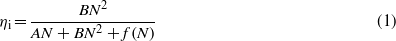
where ηi represents the device internal quantum efficiency and N is the carrier density in the device's active region. The Shockley–Read–Hall (SRH) nonradiative recombination and radiative recombination coefficients are described by A and B, respectively. f(N) is generally used to describe any other higher-order carrier loss processes, such as Auger recombination and electron overflow. Mathematically, it can be written as CN3 + DN4. In nanowire devices, due to the highly effective lateral stress relaxation associated with the large surface areas, it is expected that both the polarization fields and dislocation densities can be significantly reduced. However, the presence of surface states and defects, due to the large surface-to-volume ratios of nanowires, can contribute significantly to the carrier loss in nanowire LEDs. Additionally, it has remained debatable whether Auger recombination plays an important role on the performance of GaN-based devices [9, 16, 22, 23].
In this context, we have performed a detailed investigation of the temperature-dependent carrier recombination processes in GaN-based nanowire LEDs. Self-organized InGaN/GaN quantum dots are incorporated in nearly defect-free GaN nanowires to achieve white-light emission. To evaluate the impact of Auger recombination on the performance of nanowire LEDs, a p-doped AlGaN electron blocking layer (EBL) is incorporated between the quantum dot active region and the p-GaN region, which can effectively reduce other third- or higher-order carrier loss mechanisms due to electron overflow [24–27]. It is observed that efficiency drop is absent in such novel phosphor-free white LEDs in the temperature range from 6 to 440 K. The Auger coefficient is derived to be in the range of ∼10−34 cm6 s−1 or less, which is nearly four orders of magnitude smaller than the commonly reported values in InGaN/GaN quantum well LEDs [16, 17, 28], suggesting that Auger recombination plays an essentially negligible role in the performance of InGaN/GaN dot-in-a-wire LEDs. However, it is observed that the performance of such nanowire LEDs suffers severely from SRH recombination, which accounts for nearly 40% of the total recombination under injection current of ∼100 A cm−2 at room temperature. The carrier nonradiative lifetime is estimated to be in the range of a few nanoseconds at room temperature, which correlates well with the surface recombination velocity of GaN and the wire diameters used in this experiment [29]. This work has elucidated the primary carrier loss mechanisms in GaN-based nanowire LEDs and also provides a critical insight for the design and development of practical nanowire devices.
2. Experimental details
Illustrated in figure 1(a), a phosphor-free InGaN/GaN nanowire white LED was fabricated on an n-type Si(111) substrate. The nanowire LED heterostructure, schematically shown in the inset of figure 1(a), was grown by plasma-assisted molecular beam epitaxy without using any foreign metal catalyst. The top and bottom segments of GaN nanowires are doped p- and n-type using Mg and Si, respectively. The device active region consists of ten vertically aligned InGaN/GaN quantum dots. Each dot has a height of ∼3 nm and is capped by ∼3 nm GaN barrier layer. We have recently demonstrated that high efficiency, intrinsic white-light emission can be achieved from such nanowire LEDs by varying the sizes and/or compositions of the dots in a single epitaxial growth step [2, 8]. Additionally, a p-doped AlGaN EBL is incorporated between the quantum dot active region and the GaN:Mg segment. The use of such an EBL can effectively reduce electron leakage/overflow from the device active region [25, 27, 30, 31]. Detailed growth conditions for the dot-in-a-wire LEDs are described elsewhere [2, 8, 24].

Figure 1. (a) Schematic illustration of InGaN/GaN dot-in-a-wire LED fabricated on n-type Si(111) substrate. The device heterostructure is shown in the inset. (b) A 45° tilted scanning electron microscopy image of the InGaN/GaN dot-in-a-wire LED heterostructures grown on Si(111). (c) Bright-field TEM image and EDXS analysis of a single InGaN/GaN dot-in-a-wire structure, wherein the AlGaN EBL and InGaN/GaN quantum dots are identified. (d) Room temperature photoluminescence spectrum of the nanowire LED heterostructure.
Download figure:
Standard imageIllustrated in figure 1(b), the nanowire arrays exhibit a high degree of size uniformity and are suitable for the fabrication of large-area devices directly on Si substrates. Structural properties of the InGaN/GaN dot-in-a-wire heterostructures were further characterized by a CM200 microscope with acceleration voltage of 200 kV. Figure 1(c) shows the bright-field transmission electron microscopy (TEM) image of a dot-in-a-wire heterostructure, wherein ten InGaN quantum dots and an AlGaN EBL can be clearly identified. Shown in figure 1(c), the energy dispersive x-ray spectrometry (EDXS) analysis together with the annular dark-field image confirm the existence of multiple InGaN/GaN quantum dots. The thickness of the AlGaN EBL is ∼8 nm and the Al composition of the electron blocking layer is estimated to be ∼15%. The dot-in-a-wire LED heterostructures exhibit excellent optical properties. Shown in figure 1(d) is the photoluminescence spectrum measured at room temperature using a 405 nm laser. The emission spectrum covers nearly the entire visible wavelength region, with the peak centered at ∼550 nm. Such dot-in-a-wire nanoscale LED heterostructures can exhibit relatively high internal quantum efficiency (∼30%–60%) at room temperature [2, 8, 32].
Large-area nanowire LEDs, schematically shown in figure 1(a), were fabricated using standard photolithography, etching and contact metallization techniques. In this process, a polyimide resist was first spin-coated to fully cover the nanowires for surface planarization, which was then etched with O2 plasma to reveal top portions of the wires. The p- and n-metal contacts consist of Ni (5 nm)/Au (5 nm) and Ti (20 nm)/Au (120 nm), which were deposited on the nanowire surface and the backside of the Si substrates, respectively. Subsequently, a 150 nm indium tin oxide (ITO) layer was coated on the device's top surface to serve as a transparent electrode and current spreading layer. The fabricated devices with Ti/Au and Ni/Au contacts were annealed at ∼500 °C for 1 min in nitrogen ambient and the complete devices with ITO contact were annealed at 300 °C for 1 h in vacuum.
3. Results and discussions
Output characteristics of nanowire LEDs with areal size of ∼300 × 300 µm2 were measured under pulsed biasing conditions in the temperature range of 6–440 K. The use of pulsed biasing measurement (duty cycle of ∼0.1%) can drastically reduce the junction heating effect. Figure 2(a) shows the normalized electroluminescence spectra measured under various injection current levels at room temperature. The devices can exhibit strong white-light emission with broad spectral linewidths (full width at half-maximum ∼145 nm), due to the compositional variations of the dots in the active region [8]. The device emission characteristics are further illustrated in the chromaticity diagram under various injection currents (300–800 mA), shown in figure 2(b). The derived x and y values vary in the ranges of ∼0.34–0.36 and 0.36–0.40, respectively. The optical image of the white-light LED is also shown in the inset of figure 2(b).

Figure 2. (a) Electroluminescence spectra of a phosphor-free InGaN/GaN dot-in-a-wire white LED measured under various injection current levels at room temperature. (b) Locations of the light emission characteristics shown in the 1931 Commission International de l'Eclairage chromaticity diagram at injection currents from 300 to 800 mA. The optical image of the white LED is shown in the inset.
Download figure:
Standard imageThe relative external quantum efficiency (in arbitrary units) was derived by dividing the integrated electroluminescence intensity by the corresponding injection current density. Shown in figure 3(a) are variations of the relative external quantum efficiencies with injection currents in the temperature range of 6–440 K, which exhibit two distinct characteristics. The first remarkable feature is that the nanowire white LEDs are free of efficiency drop even under very high injection conditions (up to ∼1000 A cm−2 or larger), compared to the commonly observed efficiency drop of conventional GaN-based quantum well LEDs [33, 34]. Second, it is seen that, with increasing current, there is a very slow rise in the quantum efficiency. For example, the efficiency reaches the maximum value at an injection current density of ∼280 A cm−2 at room temperature, which is nearly a factor of ten times larger than the commonly reported values for conventional GaN-based quantum well LEDs [10, 11, 17]. The injection current at which the quantum efficiency reaches ∼80% of its peak value is plotted as a function of temperature in figure 3(b). It is seen that this critical current density increases significantly with temperature. The very slow rise of the quantum efficiency has been commonly reported in nanowire LEDs [2, 8, 9]. For comparison, the current densities at which conventional blue-emitting InGaN/GaN quantum well LEDs reach their peak efficiency are generally in the range of <15 A cm−2 [10–12, 34, 35], which, together with other reported values of GaN-based nanowire LEDs are also shown in figure 3(b).

Figure 3. (a) Variations of the relative external quantum efficiencies (EQE) with injection current densities measured in the temperature range of 6–440 K. The simulated internal quantum efficiencies (IQE) using the ABF model are also shown for comparison. (b) Plot of the current densities (solid squares) at which the quantum efficiency reaches ∼80% of its peak value as a function of temperature. The current densities at which conventional GaN-based quantum well LEDs (solid circles and triangles) and other reported GaN-based nanowire LEDs (star) reach their peak quantum efficiencies are also shown for comparison. The solid circles, upward triangles, downward triangles and star denote the data obtained from [10–12, 9].
Download figure:
Standard imageIn order to understand these unique emission characteristics, we have evaluated the radiative and nonradiative recombination processes in GaN-based nanowire LEDs using the internal quantum efficiency model described in equation (1). The calculated results are plotted as the solid curves in figure 3(a), which are in excellent agreement with the experimental data. The absence of efficiency drop in the dot-in-a-wire LEDs is first investigated. From the simulation studies, the C coefficient is estimated to be in the range of ∼10−34 cm6 s−1. For conventional GaN-based quantum well LEDs, the presence of efficiency drop is generally attributed to the third- or higher-order carrier loss mechanisms, including Auger recombination, electron overflow, carrier leakage and/or polarization fields. For III-nitride nanowire devices, however, strain-induced polarization fields can be drastically reduced, due to the highly effective lateral stress relaxation related to the large surface-to-volume ratios [1, 32, 37]. Additionally, for the present nanowire LED design, an AlGaN EBL is incorporated between the quantum dot active region and the p-GaN, which can greatly minimize or largely prevent electron overflow [24–27]. To further evaluate the significance of Auger recombination, we have compared the derived C coefficient with the commonly reported Auger coefficients in GaN-based materials and devices, shown in table 1. It is seen that the derived C coefficient (∼10−34 cm6 s−1) in this experiment is nearly four orders of magnitude smaller than the commonly reported values in InGaN quantum well heterostructures [17, 28, 34], thereby suggesting that Auger recombination plays an essentially negligible role on the performance of the present InGaN/GaN dot-in-a-wire LEDs even under relatively large injection conditions. Compared to conventional InGaN/GaN quantum well planar heterostructures, InGaN/GaN nanowire heterostructures are nearly free of defects and dislocations. As a consequence, defect-assisted Auger recombination, which may be dominant in conventional planar LED heterostructures, is expected to be negligibly small in nanowire devices. This observation is also consistent with recent theoretical and experimental studies [9, 22]. Additionally, the strong carrier confinement offered by the unique dot-in-a-wire nanoscale heterostructure may contribute to the greatly suppressed Auger recombination [38]. It is also important to notice that, without the incorporation of a suitable AlGaN EBL, significant electron overflow/carrier leakage was observed in GaN-based nanowire LEDs, which can lead to efficiency drop under relatively high injection conditions [24].
Table 1. List of commonly reported Auger coefficients in InGaN/GaN heterostructures.
| Materials | λ (nm) | C (cm6 s−1) |
|---|---|---|
| InGaN/GaN [28] | 450 | 0.35 × 10⁻³⁰ |
| In0.22Ga0.78N/GaN [34] | 480 | 2.0 × 10⁻³⁰ |
| InGaN/GaN [36] | 450 | 1.0 × 10⁻³⁰ |
| In0.10Ga0.90N/GaN [17] | 410 | 1.5 × 10⁻³⁰ |
| In0.15Ga0.85N/GaN [16] | 440 | 2.0 × 10⁻³⁰ |
| InGaN nanowire [9] | 500 | 6.1 × 10⁻³² |
| InGaN/GaN disc-in-a-wire [9] | 500 | 4.1 × 10⁻³³ |
The slow rising trend of the quantum efficiency observed in nanowire LEDs can be explained by the large SRH recombination. Illustrated in figure 4 is the derived contribution of SRH recombination to the total carrier recombination versus injection current measured at various temperatures. It is seen that the SRH recombination can account for more than 30% of the total recombination even at low temperatures under low injection conditions. With increasing temperature, the SRH recombination becomes appreciably more important. For example, under an injection current of ∼100 A cm−2, the SRH recombination accounts for ∼8%, 40% and 80% of the total recombination at 6 K, 300 K and 440 K, respectively. The significantly enhanced SRH recombination with temperature explains the drastically increased current density at which the quantum efficiency reaches its peak value at elevated temperatures, illustrated in figure 3(b). It also leads to the reduction of the maximum achievable quantum efficiency with increasing temperature, shown in figure 3(a).

Figure 4. Plot of the SRH recombination contribution versus injection current in the temperature range of 6–440 K.
Download figure:
Standard imageTo further understand the significance of SRH recombination, we have plotted the derived A coefficients as a function of temperature, shown in figure 5. It is seen that the values of A vary from ∼5.5 × 10⁷ to 4.6 × 10⁸ s−1 from 6 to 440 K, with the corresponding SRH nonradiative lifetimes in the range of ∼18.3–2.2 ns. At room temperature, the A coefficient is approximately 1.8 × 10⁸ s−1, which is significantly larger than the commonly reported values (∼107 s−1) of conventional InGaN/GaN quantum well LEDs [11, 36, 39]. This observation is in direct contrast to the drastically reduced defect densities associated with nanowire heterostructures. The somewhat unexpected large nonradiative recombination of nanowire LEDs, however, can be qualitatively understood by considering carrier recombination on the lateral surfaces. Due to the extremely large surface-to-volume ratios and the presence of surface states and defects, nonradiative carrier recombination on the wire surfaces may become appreciable. Detailed studies further confirm the presence of band bending on the lateral surfaces of GaN nanowires, which can lead to further enhanced surface recombination [40]. Additionally, the significant nonradiative surface recombination may be related to the hot carrier effect [18, 41], ineffective electron confinement [42] and poor hole transport [21] of GaN-based LED heterostructures as well.

Figure 5. Variation of the SRH nonradiative recombination coefficient (A) with temperature. The corresponding nonradiative recombination lifetimes at different temperatures and the theoretical fit using a trap energy of ∼0.063 eV separated from the intrinsic Fermi level are also shown in the inset.
Download figure:
Standard imageThe commonly reported surface recombination velocity on GaN surfaces is in the range of ∼103–104 cm s−1 [43, 44]. In the present study, the average radius of GaN nanowires is ∼40 nm. Therefore, the A coefficient, due to carrier surface recombination, is estimated to be in the range of ∼108–109 s−1, which agrees quantitatively well with the simulated results shown in figure 5. Variations of the SRH nonradiative lifetime versus temperature are also plotted in the inset of figure 5. By comparing this temperature dependence and the following theoretical model [45]:
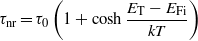
where ET and EFi denote the trap energy and the intrinsic Fermi level, respectively, we have derived that the trap energy level is separated from the intrinsic Fermi level by ∼0.063 eV. However, the exact nature of the trap states and defects needs to be further investigated.
Clearly, the surface SRH recombination, if not remediated, can severely degrade the performance of nanowire LEDs. It can lead to a very slow rise in the quantum efficiency and further limits the maximum achievable efficiency at high injection levels. Detailed studies further show that the performance of nanowire LEDs without the incorporation of an AlGaN EBL suffers considerably from electron overflow/leakage under relatively large injection conditions [24]. The resulting efficiency drop, however, may be less dramatic, compared to conventional quantum well LEDs, due to the large influence of nonradiative surface recombination. Significantly improved device performance can be possibly achieved by embedding the InGaN/GaN dot-in-a-wire in a large bandgap AlGaN shell structure to minimize nonradiative recombination on the wire surfaces [37, 46], while maintaining the benefits associated with the large surface-to-volume ratios of nanowire LEDs.
4. Conclusion
In conclusion, through detailed analysis of the temperature- and current-dependent electroluminescence of InGaN/GaN nanowire LEDs, we have demonstrated that SRH recombination, due to the large surface-to-volume ratios and the presence of surface states and defects, is largely responsible for the unique characteristics of GaN-based nanowire LEDs. Detailed studies further confirm that, for nanowire LEDs with the incorporation of a suitable EBL, any third- or higher-order carrier loss mechanisms can become essentially negligible, thereby leading to phosphor-free white LEDs that are free of efficiency drop even under very large injection conditions. This work provides unambiguous evidence that Auger recombination plays an essentially negligible role in the performance of InGaN/GaN dot-in-a-wire LEDs. It further elucidates the role of nonradiative recombination in the performance limit of nanowire LEDs and offers critical insight for the future development of practical nanowire photonic devices.
Acknowledgments
This work is supported by the Natural Sciences and Engineering Research Council of Canada (NSERC), the Fonds de recherché sur la nature et les technologies (FQRNT), MDEIE—Programme de soutien à la valorisation et au transfert and McGill University. Part of the work was performed in the McGill University Micro Fabrication Facility. Some of the TEM work was carried out at the Canadian Centre for Electron Microscopy, a national facility supported by the NSERC and McMaster University.