

Abstract
Co3O4 samples have been deposited using RF-magnetron sputtering from an oxide target. In situ x-ray and ultraviolet photoelectron spectroscopy and x-ray diffraction have been carried out to identify the phase and composition of the films. The work function of  films showed variation of about 1 eV depending on the oxygen content of the sputter gas while the Fermi level position in the band gap was invariant towards different deposition parameters. Optical transmission spectroscopy in the UV/VIS/NIR regime showed two optical transitions at 0.8 eV and 1.7 eV. However, the optical absorption from these transition does not seem to aid in the conduction of charge carriers as has been revealed by conductivity measurements in a linear 4-point-setup. Diodes were prepared in a glass
  FTO
FTO 

 NiO
NiO  Au-stacking geometry. They show poor photovoltaic behaviour with a short-circuit current of 0.33 mA cm−1 and an open-circuit voltage of 0.15 V, resulting in an overall efficiency of
  . The limitation of
  as an absorber in an All-Oxide solar cell can be related to poor transport properties combined with defect states in the band gap and Fermi level pinning at interfaces.
Export citation and abstract BibTeX RIS
1. Introduction
Transition metal oxides (TMOs) offer a variety of interesting properties, which are often related to interaction of correlated electrons in the cation d-shells [1, 2]. An intensively studied TMO is  , which has been considered to be used as selective coating for solar photothermal converters [3], catalyst [4], magnetic material [5], sensor [6], and absorber in a solar cell because of a band gap of a suitable range [7, 8] which is not the case for many other oxides such as e.g.
  [9]. In addition, more fundamental studies on the optical, structural, magnetic, and electrical properties have been performed [10–16]. The interesting properties of
  originate from its electronic structure, which is mainly derived from the crystal field and exchange interaction split cobalt 3d-states. The electronic structure has been under discussion for quite a while and has been studied by means of photoelectron spectroscopy (XPS) [16–18] and computational methods [19–21].
 crystallizes in the normal spinel structure with a lattice parameter of 8.08 Å [22]. The unit cell consists of an fcc-lattice of O−2-ions with one half of the octahedral sites filled by Co+3-ions and one eighth of the tetrahedral sites occupied by Co+2-ions, respectively [23]. Due to the different coordinations of the cations the degeneracy of the 3d-orbitals is lifted by crystal field splitting (figure 1). The five 3d-states of the Co+3-ions are split into three degenerate fully occupied t2g-states and two degenerate empty eg-states, whereas the 3d-electrons of the Co+2 are distributed among the two lower lying, fully occupied e-state and the three half-filled t2-states, respectively [24]. Furthermore, exchange interaction caused by the unpaired electrons in the Co+2 t2-states lifts the degeneracy even further.
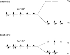
Figure 1. Crystal field splitting for the octahedral coordinated Co+3-ions and the tetrahedral coordinated Co+3-ions.
Download figure:
Standard image High-resolution imageIn this work structural, optical, and electronic properties of RF-magnetron sputtered  thin films were investigated with regard to their application in solar energy conversion devices.
  was chosen as material because of the suitable size of band gap for solar cell absorbers and because of its potential suitability as a parent material for more complex oxides. Here, the behavior of the parent materials have to be understood well. As interfaces strongly influence such devices the interface formation of
  towards ITO and
  was determined in addition.
2. Methods
The samples were prepared at the DArmstadt Integrated SYstem for MATerial Research (DAISY-MAT) [25] by means of RF-magnetron sputtering from a  target with a diameter of 5.08 cm on bare and ITO-coated glass substrates with dimensions of
  mm, each. For each deposition one of each substrate was cleaned thoroughly with isopropanol, a cleansing agent, and distilled water before being mounted together onto a stainless steel holder and being loaded into the UHV system. The preparation parameters for the
  samples can be found in table 1.
Table 1. Deposition parameters for  samples and the contact materials
  and ITO for interface experiments.
 |
RuO2 | ITO | |
|---|---|---|---|
| Tsub (°C) | rt-400 | rt | rt |
| p (Pa) | 0.5 | 1 | 0.5 |
| dTS (cm) | 8.5 | 9.4 | 10 |
| flux (sccm) | 10 | 10 | 10 |
| O_2/Ar ratio (%) | 0–15 | 7.5 | 0 |
| P (W) | 50 (RF) | 10 (DC) | 25 (RF) |
| R (nm min−1) | 0.3–4 | 3 | 5 |
The integration of a Physical Electronics PHI 5700 multi-technique surface analysis system into the cluster-tool DAISY-MAT allowed for the sample characterization by x-ray and ultraviolet photoelectron spectroscopy (XPS/UPS) [25]. For the former, monochromatic Al Kα radiation (1486.6 eV) was used. The energy resolution has been determined from the Gaussian broadening of a sputter cleaned Ag sample to be ≈400 meV. UPS measurements were performed with an excitation energy of 21.22 eV. Calibration of the binding energies was achieved by adjusting to the Ag 3d5/2- ( eV [26]) and Cu 2p3/2-core levels (
 eV [26]) and the Ag Fermi-edge (measured with XPS and UPS) from freshly sputter cleaned samples.
The investigations of the band alignments of  with the contact materials
  and ITO were performed in so called interface experiments [27]. Here, the contact material was deposited in a step wise process on a freshly prepared
  substrate. In between two steps the substrate and contact films were analysed using XPS. Additionally, UPS measurements were performed on the bare substrate and a thick 'bulk' contact film to determine the work functions. A more detailed description of such kind of experiment can be found elsewhere [28].
Optical properties were measured on samples deposited on bare glass substrates with a bare glass substrate as reference. The UV/VIS/NIR transmission spectra were recorded in a range of 250–3200 nm using a Perkin-Elmer Lambda 900 spectrometer. The absorption was calculated as ![$\alpha \left(h\nu \right)=-\ln \left[T\left(h\nu \right)\right]/d$](https://content.cld.iop.org/journals/0022-3727/49/15/155306/revision1/daa18b1ieqn029.gif) , where T is the measured transmission and d is the thickness of the film. The latter has been obtained by measuring the edge between deposited film and substrate at different positions of the sample using a Dektak XT profilometer.
, where T is the measured transmission and d is the thickness of the film. The latter has been obtained by measuring the edge between deposited film and substrate at different positions of the sample using a Dektak XT profilometer.
Structural analysis was performed by means of X-Ray diffraction using a Seifert XRD 30003 PTS-3 diffractometer in  -geometry with Cu Kα radiation.
Electrical properties were measured in a four-point-setup on samples on bare glass substrates. The samples were measured both in the dark and under an AM 1.5g illumination from a solar simulator from (LOT, Darmstadt, Germany).
Diodes were prepared in a glass  FTO
FTO 

 NiO
NiO  Au-stacking geometry. The difference in work function of FTO and Au is being used to create an internal potential which separates generates charge carriers in this pin-like structure [7].
  and NiO act as electron and hole blocking layer, respectively. Cells without
  or NiO were short circuited. jU-characteristics were measured illuminated with a power density of 1000 W m−2 and in the dark.
3. Results & discussion
3.1. Phase characterisation
Freshly prepared  samples have been characterized in situ with XPS. Typical XP spectra for
  are shown in figure 2 from a sample that has been prepared at 400 °C with 1% oxygen in the sputter gas. The survey spectra in the upper graph of figure 2 shows no signal from contaminations as carbon. Peaks have been labelled according to their binding energies [26].
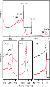
Figure 2. XP spectra of  from two samples which were deposited at 400 °C without (dashed line) and with 1% (solid line) of oxygen in the sputter gas. The survey spectra in the upper graph shows the survey spectrum of the sample which has been deposited with 1% of oxygen in the sputter gas.
Download figure:
Standard image High-resolution imageA more detailed view on the XP spectra can be found in the lower graphs of figure 2. Here, characteristic peaks of two samples deposited at 400 °C without (dashed line) and with 1% oxygen in the sputter gas are shown. The Co 2p-doublet of the sample with oxygen on the left-hand side can be found at binding energies of 779.36 eV and 794.41 eV. These binding energies as well as their difference of about 15 eV agree well with literature [16, 22]. The same applies for the satellite structure of the Co 2p3/2 peak, which consists of a superposition of satellites at binding energies about 10 eV (arrow A) and 6 eV (arrow B) away from the main line, respectively. As the former has been assigned to the Co3+ -ions and the latter to the Co2+ -ions, their existence shows the presence of both valencies [16, 22].
The sample without oxygen shows binding energies of the two main lines of 779.51 eV and 794.58 eV, which are slightly higher but show the same difference of about 15 eV. However, the satellite structure is different. The satellite at 6 eV away from the main line (B) seems to be more pronounced compared to the satellite at 10 eV (A) away from the main line. This indicates a different ratio of the divalent cobalt cation towards a more reduced state with more Co2+ . This conclusion makes sense as oxygen might get lost during the deposition and would need to be replaced from the gas.
The O1s peaks in figure 2 show a binding energy of 529.63 eV for the sample with oxygen and 529.79 eV for the sample without oxygen, respectively. As the binding energy of the former agrees well with values found in the literature [16, 22] and the shift of the latter is as large as for the Co 2p-doublets, the same argumentation of a reduced sample can be used here as well.
The valence band on the right-hand side shows a sharp peak at the valence band maximum for both samples. This peak consists of a superposition of Co3+ 3d- and Co2+ 3d-electrons [21]. The VBM has been assigned to Co2+ eg orbitals with minority spin by Qiao et al [21], which could be determined from a linear extrapolation of the low binding energy part of the peak to be 0.28 eV for the sample with oxygen in the gas and 0.4 eV for the sample without oxygen, respectively. Other samples that have been deposited with higher percentage of oxygen showed valence band maxima of 0.3 eV or lower as well, indicating the already reported p-type behaviour [11] of  , if a band gap of 0.8 eV (see figure 6) is considered. The higher valence band maximum of the sample without additional oxygen can be traced back to a reduction as it has been already seen in the Co 2p spectra.
For a better understanding about the role of additional oxygen in the deposition on the surface of a sample, UPS measurements with He I radiation were performed. The spectra are shown in figure 3 and indicate a shifting of the secondary electron edge (SEE) of about 1 eV to lower binding energies by the addition of oxygen. From the position of the SEE, the work function ϕ can be calculated as  and results in values of 4.65 eV for the sample prepared without addition of oxygen and of 5.69 eV for the sample prepared with 1% of oxygen, respectively. Addition of higher percentages of oxygen into the sputter gas did not result in higher work functions.
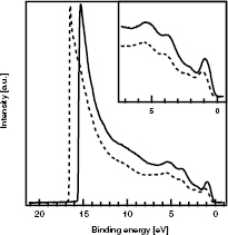
Figure 3. UP spectra for a sample deposited using Ar (dashed line) and a 1% O2/Ar mix (solid line) as sputtering gas, respectively. The inset shows the valence band region.
Download figure:
Standard image High-resolution imageXRD measurements (figure 4) on both samples revealed a crystalline  phase with a (1 1 1)-texture for both. The difference in work function does therefore not indicate a different crystallographic phase. However, the higher work function can be attributed to the higher oxygen content, of the deposition atmosphere which can lead to a different oxygen termination of the surface, thereby changing the work function.

Figure 4. XRD pattern of two  samples sputtered without (top) and with 1% oxygen (bottom) in the sputter gas. The reflexes were identified using
  pdf-card-2-00-080-1533 as reference.
Download figure:
Standard image High-resolution imageBesides the small shifts to higher values the Fermi energy showed an invariance towards the deposition conditions, e.g. the oxygen content of the sputter gas. This is shown in figure 5 for samples deposited with parameters shown in table 1. The arbitrary ordering on the abscissa reflects the different samples. The valence band maxima EVBM were measured with XPS and the conduction band minima ECBM calculated with a band gap value of 0.8 eV from optical measurements. The Fermi level EF was set to be zero and the vacuum level was placed above EF by the value of the work function ϕ from UPS measurements. As can be seen, the position of the Fermi level cannot be shifted freely through the band gap but is pinned to values below the midgap position indicating p-type behaviour. Materials exhibit a pinning of the Fermi level, if defect states with energies within the band gap are present [29]. The exact nature of these defects was not determined for  .
.
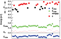
Figure 5. Band edges and vacuum level for  samples sputtered with parameters from table 1. The abscissa represents an arbitrary ordering of the samples. The Fermi level of the samples was set to zero.
Download figure:
Standard image High-resolution image3.2. Opto-electronic properties
The transmission curve of a  sample deposited at 400 °C with 1% oxygen in the sputter gas is shown as a solid line in figure 6. Similar results were found for other films of
  which were deposited at different temperatures and oxygen contents and in the literature [21]. Neglecting reflection, from the transmission data the absorption coefficient α could be calculated and is shown as the point-dashed curve in figure 6. It shows two maxima at 0.8 eV and 1.7 eV. These agree very well with optical transitions of
  that can be found in literature [15]. Surprisingly, the absorption coefficient increases again for small photon energies. An influence of interference effects due to the thickness of the sample could be ruled out as similar effects were observed for different thicknesses. However, the observation might indicate a lower fundamental gap or defect levels in the band gap, which contribute to absorption at these energies as well. A lower fundamental gap or a high defect concentration in the gap is also consistent with electrical measurements using a 4-point setup with and without an AM1.5 illumination from a solar simulator. Temperature dependent conductivity measurement revealed a semiconducting behaviour with a room temperature conductivity below 1 S cm−1 and an activation energy of about 0.18 eV for a variety of films deposited at different temperature and oxygen contents. Nevertheless, no change of conductivity under illumination could be observed which could be explained by a fast recombination of photogenerated carriers due to high bulk defect densities. Similar conductivities at room temperatures are reported in literature [12] and indicate that the limitation of the transport properties are of intrinsic nature.

Figure 6. UV/Vis/NIR transmission spectra (solid line) and absorption coefficient (point-dashed line) over the photon energy of a  (400 °C/1% oxygen) sample.
Download figure:
Standard image High-resolution imageThe jU-characteristics of a diode prepared in a glass  FTO
FTO 

 NiO| Au-stacking geometry are shown in figure 7 for a measurement in the dark and under AM1.5g illumination. Here, FTO and Gold act as front and back contact, respectively. The
  absorber was prepared at 400 °C with an oxygen content of 1% in the sputter gas. From the curve in figure 7, it is obvious that the cell suffers from a poor short-circuit current density jSC of 0.33 mA cm−1 and a low open-circuit voltage UOC of 0.15 V. Similar values can be found for solar cells with a
  absorber in literature for deposition temperatures up to 300 °C [8]. Higher open-circuit voltages for cell based on an absorber deposited at 600 °C could not be obtained as the films were not stable at this temperature but were rather composed of
  and CoO.
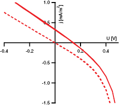
Figure 7. IU-characteristic for a solar cell in a glass  FTO
FTO 

 NiO
NiO  Au-stacking geometry. The
  absorber of this cell was deposited at 400 °C with 1% oxygen in the sputter gas.
Download figure:
Standard image High-resolution imageThe current density is likely limited by the transport properties of the Co 3d orbitals which form the band edges [14] of the material. Due to strong localization and hopping transport in these orbitals, low mobilities have been reported for  and other TMOs in literature [30–32]. Efforts to measure the Hall-mobility were not successful due to the low values. The low mobility of the charge carriers combined with the proposed recombination through high defect density will result in a low charge carrier life-time. The low open circuit voltage UOC can be explained by interface properties which will be presented in the following section. Overall, these limitation result in a low fill factor of 24% and an efficiency of
  .
.
3.3. Interface experiments
Figure 8 shows the development of the valence band and core level spectra for a stepwise deposition of metallic  (top) and ITO (bottom) onto a
  substrate, respectively. The contact materials were chosen as model materials for high (
 ) and low (ITO) work function materials to represent a pin-like structure, respectively. As expected, the substrate signal decreases in both cases while the film signal intensifies. Also shown is the change of the valence band from the
  -VB to
  or ITO, respectively. For intermediate times, the VB signal is a superposition of substrate and film material. Therefore, the position of the VBM cannot be extracted from a direct measurement. However, under the assumption that the distance of a distinct core level to the VBM of a defined material is a constant [27, 28], the shift of a core level during such an experiment reveals the position of the VBM after each deposition step.
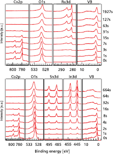
Figure 8. Core-level and valence band spectra of the contact materials  (top) and ITO (bottom) and the substrate
  of the two interface experiments.
Download figure:
Standard image High-resolution imageThe positions of the valence band maximum after each deposition step for the two interface experiment are shown in figure 9. The dashed lines show the valence band position for  when being stepwisely covered with
  . Here, the VBM shifts from an initial position of 0.34 eV to a final distance to the Fermi level of 0.57 eV, which results in a downward band bending of 0.23 eV.
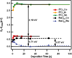
Figure 9. Positions of the valence band maxima of ITO (solid lines),  (dashed lines), and the two
  substrates of the interface experiments, respectively. The positions have been derived from the shift of the Co 2p3/2, Ru 3d5/2, In 3d5/2, and Sn 3d5/2 as shown in figure 8.
Download figure:
Standard image High-resolution imageThe solid lines in figure 9 indicate the valence band position of  (square markers) and ITO (triangular, round markers). Here, the VBM of
  shifts from an initial position of 0.34 eV away from the Fermi level to a final position at the interface of 0.71 eV. As the VBM of ITO shifts parallel to the VBM of
  for small deposition time, this shift can be explained by a shift of the Fermi level in the substrate
  [28]. Therefore, it is concluded that the VBM of ITO does not change which is reasonable due to the high charge carrier concentration of this degenerate semiconductor [31]. From a parallel part of the respective graphs, the distances of the valence band maxima can be extracted. The value of 2.18 eV is shown in figure 9 and agrees very well with values for other transition metal oxides in contact to ITO [9, 31, 32].
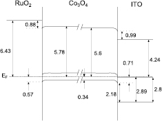
From UPS measurements the work functions of the non-covered  substrates and 'bulk' contact materials could be determined. Combined with the VBM from XPS and the band gaps for ITO of 2.8 eV from literature [33] and
  of 0.8 eV from optical measurements, respectively, band diagrams of the two interfaces could be drawn. These are shown in figure 10.
Figure 10. Band diagrams for interfaces of  towards
  (left) and ITO (right), respectively.
Download figure:
Standard image High-resolution image
On the left-hand side the interface of  towards
  is shown. Here, a surprising downwards bending of the VBM of
  is observed. However, on-going investigations seem to indicate that the measured high work function of
  of 6.43 eV is related to adsorbed oxygen [34] and therefore, does not reflect the situation at the interface perfectly. Actually, the effective work function might be much lower (≈ 5–6 eV), which would explain the downward bending and high vacuum level offset of 0.88 eV. Usually, this value can be explained by the formation of interface dipoles due to unsaturated bonds [35–37].
The bands at the interface to ITO are shown on the right-hand side of figure 10. Here, a downward bending of the  -VB is observed as can be expected from the difference in work function of the two materials. Again, a large interface dipole of 0.99 eV is observed.
The VBM position of  at the interfaces to the two contact materials with strongly different work function is very similar. For other materials like
  [9, 32],
  [32, 38] or Pb(Zn,Ti)O3 [32, 39], much higher differences to
  and ITO have been observed. Therefore, it can be concluded that the Fermi level at the interface of
  is pinned to a high degree. Hence, the position of the VBM cannot be manipulated a lot. The pinning of the Fermi level is the reason for the poor photovoltaic behaviour, in particular the low photovoltage. Whether these pinning states result from bulk defect states originating from oxygen deficiencies or are due to Co2+ or Co3+ derived surface states with reduced O-coordination on surface sites need further experiments for a detailed analysis.
4. Conclusion
 films were deposited with RF-magnetron sputtering from an oxide target. Depending on the oxygen content in the sputter gas the work function could be changed by about 1 eV. The opto-electronic properties of the film showed a first optical transition at 0.8 eV but almost no changes of the conductivity due to illumination. Solar cells with
  as absorbers showed only small current densities and voltages. While the former can be related to poor transport properties within the Co 3d-orbitals, the latter is related to Fermi level pinning at interfaces of
  . Both can be explained by the defect structure of
  or potentially also by electron correlation effects. Therefore, they can be regarded as intrinsic properties of
  .
.
Acknowledgments
Financial support from the European Commission under the FP7 AllOxidePV project 'Novel Composite Oxides by Combinatorial Material Synthesis for Next Generation All-Oxide-Photovoltaics', number 309018 is gratefully acknowledged.