
Abstract
We present a study on the growth of a low-density ordered Ge quantum dot (QD) on a nanohole patterned Si (0 0 1) substrate with periods in the order of microns by molecular beam epitaxy. Ordered Ge QDs with different periods were realized, the largest period being 15 µm. From the height-profile evolution of the QD with Ge deposition, it was found that the nanohole filling started at the initial Ge deposition, indicating an immediate nucleation and growth of QDs inside the nanoholes. Such a phenomenon is attributed to a lower surface chemical potential (SCP) inside the nanoholes, which is supported by calculated results on SCP evolution with growth and verified by the observation that the Ge adatoms around the nanoholes exhibited a higher probability of being incorporated into the nanoholes. In this scenario, low density ordered Ge QDs with any large periods could be achieved. The optical properties of the Ge QDs showed a remarkable improvement after a post-growth rapid thermal annealing treatment.
Export citation and abstract BibTeX RIS
1. Introduction
The growth of ordered Ge quantum dots (QDs) has attracted considerable attention owing to their potential applications in novel optoelectronic devices [1, 2]. Advances in semiconductor lithography technologies offer the unique capability of positioning QDs in specific sites by substrate patterning [3–12]. Various kinds of micro-structured substrate surfaces, including concave nanoholes and trenches [3, 5, 6, 9, 10], convex ridges [8–10], vicinal surfaces [11] and SiO2 windows [12], have been demonstrated to be effective ways of controlling the QD site and uniformity. This is beneficial as two kinds of interesting QD systems could be realized. One is the three-dimensional (3D) ordered and uniformed Ge QD ensemble with strong inter-QD electronic state coupling (also namely the quantum dot crystals), in which carrier minibands are formed and thus lead to enhanced interband oscillator strength [3, 5, 13–15]. The other is site-controllable low density Ge QDs with large periods, which are highly desirable for specific applications based on a single Ge QD, e.g. the single-electron transistors [16] and the photonic crystal microcavity integrated quantum optical devices [17–19]. The large in-plane period benefits the integration of various kinds of resonant microcavities with a single QD.
Considerable effort has been devoted to the molecular beam epitaxy (MBE) growth of two-dimensional (2D) ordered Ge QDs [3, 5, 6, 8, 10, 20–22]. Among them, however, very few have been concerned with the growth in low-density regime. Secondary-QD nucleation on the flat regions between nanoholes has frequently been observed on patterned Si substrate with various periods [20, 21, 23], which is detrimental to the QD ordering. Different mechanisms for the QD ordering and the Ge adatom surface diffusion on patterned Si substrate have been proposed. In small period regime, Zhong et al proposed that the 2D QD ordering is kinetically determined by the mismatch between the Ge adatom surface diffusion length (Ld) and the pattern period (P) at different growth temperatures [23]. In contrast, in large-period regime, Grydlik et al proposed that Ge adatoms could pass, on average, a thousand nanoholes before they were incorporated into one [21, 24]. For the growth of low-density ordered Ge QDs, several fundamental questions remain to be answered, e.g. how large period could be realized? Are there limits for its values and, if so, reasons for those limits? Actually, the ordering mechanism for the Ge QDs at large periods is still controversial and hasn't been fully understood. A detailed investigation into the growth of low density ordered Ge QDs on patterned Si substrate is still necessary.
In this paper, we investigated the growth of low-density ordered Ge QDs on nanohole patterned Si (0 0 1) substrate with periods in the order of microns by MBE. Ordered Ge QDs with different periods were achieved at low growth temperatures of 450–550 °C, the largest period being 15 µm. The growth evolution of Ge QDs with Ge deposition clearly illustrates that the nanohole filling starts at the initial Ge deposition, indicating an immediate nucleation and a zero critical thickness for QD growth inside the nanoholes. 2D surface chemical potential (SCP) distributions for nanoholes at the corresponding growth stages were also calculated, revealing that SCP minima exist inside the nanoholes. The realization of low-density ordered Ge QDs is essential owing to the lower SCP in the nanoholes. Such a conclusion was supported by the observation that the Ge adatoms around nanoholes exhibited a higher probability of being incorporated into the nanoholes.
2. Experimental details
Electron beam lithography (EBL) and reactive ion etching (RIE) were utilized to fabricate nanohole patterns on Si (0 0 1) substrates. The Si (0 0 1) substrates were coated with e-beam resist ZEP-520A and exposed to 100 kV electrons at a beam current of 100 pA followed by the development in ZEP-N50. The patterns were then transferred to Si substrates by RIE with an O2/CF4 mixture (80 : 5) at 150 W, 4.3 Pa for 45 s. The nanoholes were periodically aligned along two orthogonal Si <1 1 0 > directions with periods ranging from 0.6 to 15 µm, and showed cylindrical shape after RIE etching. The mean depth and width of the nanoholes after processing were ∼25 and ∼90 nm, respectively. The pre-patterned Si substrates were cleaned by the standard RCA method and passivated with H by emersion in a dilute HF solution before loading into a solid-source MBE chamber (Riber Eva-32). The growth procedures of the Ge QDs are as follows. First, the patterned substrate was heated to 820 °C for 5 min to desorb the passivating H. Then a Si buffer layer was deposited at a rate of 0.3 Å·s−1 with a substrate temperature of 450 °C. The Ge QDs were then grown by depositing Ge at a rate of 0.06 Å·s−1 with the substrate temperature ramping from a low to a high value. After growth, the samples were immediately cooled down to room temperature. The surface morphologies of the samples were characterized by using atomic force microscopy (AFM) (Veeco DI Multimode V SPM). For photoluminescence (PL) measurements, the samples were placed in a closed-cycle helium cryostat with a temperature range from 16 K to room temperature. An Ar+ laser (488 nm) was used as the excitation source. The laser spot size is ∼500 µm2. The PL spectra were recorded by a wavelength extended InGaAs detector using the standard lock-in technique. For composition analysis, the 2D scanning Auger elemental map (SAM) for the Ge QDs was acquired by using Scanning Auger Nanoprobe (PHI SMART-200) in CMA mode. The electron beam used in the Auger measurements had an energy of 20 keV and an incident angle of 30° to the surface normal sample.
3. Results and discussion
Figures 1(a)–(f) show the surface morphologies of the 2D ordered Ge QDs with periods of 0.6, 1, 3, 5, 10 and 15 µm, respectively. The growth parameters and the QD sizes are listed in table 1. Due to the very large ratio of the period to the QD size in figure 1(f), the QD positions are indicated by white arrows for a better view. The inset of figure 1(f) shows a high resolution AFM image (1024 × 1024 lines) on the QD site and its nearby area. Clearly, no small islands or hut clusters existed on the flat areas between the nanoholes. From figures 1(a)–(f), it is clear that very good 2D ordering for QDs was achieved for all samples. Each nanohole was filled by only one QD and no secondary islands existed on the flat regions between the nanoholes. The QDs were highly size-uniformed and pyramid or dome-shaped.
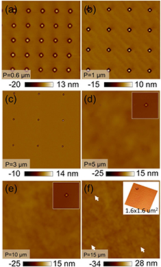
Figure 1. Surface morphology of the ordered low-density Ge QDs grown on the patterned Si substrate with a period of (a) 0.6, (b) 1, (c) 3, (d) 5, (e) 10 and (f) 15 µm, respectively. The insets in (d)–(f) are enlarged AFM micrographs of a single Ge QD in corresponding periods. The white arrows in (f) indicate the QD positions for a better view. The growth parameters and the dot sizes are listed in table 1.
Download figure:
Standard image High-resolution imageTable 1. Growth parameters and conditions for the samples shown in figures 1(a)–(e).
| Period (µm) | Buffer thickness (nm) | Buffer temperature (°C) | Ge thickness (ML) | Ge temperature (°C) | QD width/height (nm) |
|---|---|---|---|---|---|
| 0.6 | 130 | 400 | 8.5 | 450 → 550 | 144/23.4 |
| 1 | 40 | 400 → 550 | 3 | 450 → 550 | 140/18.7 |
| 3 | 40 | 400 → 550 | 3 | 450 → 550 | 138/20.2 |
| 5 | 40 | 400 → 550 | 3 | 450 → 550 | 106/15.3 |
| 10 | 40 | 400 → 550 | 3 | 450 → 550 | 108/16.7 |
| 15 | 40 | 400 → 550 | 3 | 450 → 550 | 108/17.1 |
To understand the growth of the large period ordered QDs more quantitatively, the volume per dot, dot areal density and the ratio of the total Ge amount inside QDs to the total Ge deposition (as denoted by Σdots/Σdep) were plotted as a function of the period, as shown in figures 2(a) and (b), respectively. The QD volume was roughly estimated by simply using a cone structure as shown by the inset in figure 2(a). It was found that the dot volume showed a strong decrease for periods larger than 4 µm. For the periods less than 4 µm, the dot volume is about 2.6 × 10⁵ nm3 while for the periods larger than 4 µm, the dot volume is about 1.4 × 10⁵ nm3. We speculate that such a phenomenon may be related to the different Ge adatom surface Ld at different pattern periods. Further detailed investigations are needed. The dot areal density decreased from 1 × 10⁸ to 4.4 × 105 cm−2 with the period increase from 0.6 to 15 µm. The ratio of Σdots/Σdep also dramatically decreased from ∼0.3 to nearly zero (∼ 0.004) with the increased period, which is attributed mainly to the decreased nanohole areal density and also to the decreased QD volume with the increased pattern period. It is noteworthy that a higher Ge deposition amount of 8.5 MLs was used for the nanohole pattern with a period of 0.6 µm, which was due to the growing demand for the Ge deposition amount at small periods to realize upward dome-shaped QDs.
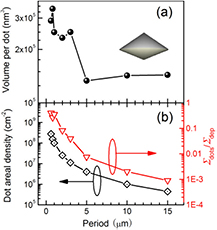
Figure 2. (a) Volume per Ge QD as a function of period. The inset shows a schematic cone structure used to estimate the volume of QDs grown inside nanoholes. (b) Dot areal density and the ratio of Σdots/Σdep as a function of period.
Download figure:
Standard image High-resolution imageThe morphology evolution of the low-density ordered Ge QDs with Ge deposition is shown in figures 3(a)–(f) for a period of 3 µm. The corresponding height profiles across the QDs are shown in figure 3(g). The plot of the height profile as a function of the Ge deposition amount is illustrated by different colors in figure 3(g). As shown in figure 3(a), the nanohole brink became smooth after Si buffer layer growth. At the Ge depositions of 0.5 and 1.5 MLs, no protruding was observed at the center of the nanoholes from the AFM images, as shown in figures 3(b) and (c). It may be concluded that no dots were formed since the Ge deposition thickness is less than a so-called 2D–3D critical thickness for dot nucleation. However, from the height profiles shown in figure 3(g), it was clearly seen that the nanohole filling with Ge adatoms started at the initial Ge deposition, and results in a gradually-shoaled nanohole, that is, the Ge QD growth in the nanoholes started at the initial Ge deposition. In this sense, the critical thickness for the QD growth in the nanoholes is zero, and the QDs nucleate immediately at the beginning of Ge deposition in the hole. The QDs formed at those two thicknesses have a downward dome shape. Figures 3(d)–(f) show QD morphologies at the Ge deposition of 2.4, 3.0 and 4.0 MLs, respectively. And the QD shape changed from a downward to an upward dome. At the Ge deposition of 4.0 MLs, the QD showed a multi-faceted superdome [25], and randomly distributed secondary Ge dots appeared on the flat regions between the nanoholes. The appearance of the secondary Ge dots clearly indicates that 4 MLs Ge has already exceeded the critical thickness for island growth of Ge on the flat regions at 450–550 °C [26]. The formation of a superdome is owing to the delayed plastic-strain energy relaxation on patterned Si substrates [22, 27].
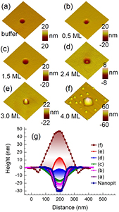
Figure 3. Surface morphology evolution of a Ge QD inside a nanohole in low-density growth regime. (a) After growth of a 40 nm-thick Si buffer layer. (b)–(f) After deposition a nominal Ge thickness of 0.5, 1.5, 2.4, 3.0 and 4.0 ML, respectively. Image size: 850 × 850 nm2. (g) The corresponding height profiles cross the QDs in (a)–(f). As can be seen, the nanohole filling and the immediate QD nucleation starts at the initial 0.5 ML Ge deposition.
Download figure:
Standard image High-resolution imageSecondary Ge dot nucleation on regions between nanoholes on patterned Si substrate has been observed at various growth conditions [20, 21, 23, 24]. The occurrence of the secondary dots is detrimental to the dot ordering and has been generally interpreted from the viewpoint of Ld. Ld can be simply estimated via a qualitative surface-diffusion model based on growth kinetics, and is given by Ld = (Dτ)1/2, D = a2νexp(−E/kBT), where D denotes the diffusion constant, τ is the time interval for adatom diffusion, a is the lateral motion (3.84 Å) corresponding to each hop of an adatom, ν is a prefactor (about 1013), E is the effective barrier for adatom diffusion on patterned substrates, kB is the Boltzmann constant, and T denotes growth temperature. In this model, the dominant part of adatom diffusion length is the effective barrier of E, which is closely related to the microstructures on the substrate surface.
Zhong et al have studied the temperature-dependent growth of ordered Ge QDs on patterned Si substrates with submicron periods [7, 23] and found that only at an intermediate temperature range around 700 °C could the growth of ordered Ge QDs be achieved. Ge adatom Ld of 160 ∼ 1100 nm were estimated at the temperature range of 600 ∼ 800 °C using a Eb of ∼1.5 eV. The ordered QD growth at around 700 °C was attributed to the comparable Ge adatom Ld to P, while the stochastic growth at higher (or lower) growth temperatures was attributed to a larger (or smaller) Ld than P. A similar ordered Ge QD growth at 650 °C on nanohole-patterned Si substrate had been reported by Grydlik et al [20, 21, 24]. However, they attributed the occurrence of the secondary-dot on the flat regions between nanoholes to the consequence of a lower Ge incorporation rate as compared to the deposition rate. They concluded that to obtain strictly-ordered islands on substrates with large periods one has to deposit an amount of Ge below the critical thickness of 4.2 MLs on flat wetting layer (WL) regions but above 3 MLs at a low growth rate of 0.03 Å·s−1. Since below this thickness atoms are very strongly bound in the WL [28], which prevents Ge diffusing to the nanoholes. By using a very low Ge deposition rate of 0.03 Å·s−1, ordered Ge QDs with a large period of 3.4 µm were achieved [21]. However, in our case, as shown in figure 3(d) the strictly-ordered QDs with a large period of 3 µm (or even 15 µm) were still achieved with a deposition amount of 2.4 MLs (smaller than 3 ML) at an even higher growth rate of 0.06 Å·s−1 (larger than 0.03 Å·s−1). In that sense, the rate model cannot adequately explain our results. In contrast, the SCP model, adopted in this paper, could provide a better explanation. At initial deposition, Ge adatoms accumulated in the holes, thus the nucleation and growth of the QDs in the nanoholes began immediately, as shown in figure 3(g). This means that the ordered QDs could be achieved at any large periods and independent of Ld to a certain extent. The 3 MLs Ge deposition in our growth is less than the 2–3D critical transition thickness on flat surfaces at 450–550 °C, thus it is reasonable that no secondary QDs would exist on flat regions. A 4 MLs Ge deposition amount already exceeded the 2–3D critical transition thickness on flat surfaces, which led to the formation of randomly-distributed secondary dots on flat regions between the nanoholes.
A kinetic model on the basis of local SCP has previously been developed in investigating the site-selective nucleation nature of Ge QDs on patterned Si substrates [9, 10, 29]. In the SCP model, the control of dot nucleation positions in heteroepitaxy is realized by a local SCP minimum, which is closely related to the spatially non-uniform relaxation of the strained energy and the variation of the surface energy due to the surface fluctuation of the epilayer. The detail of the GeSi/Si SCP model and equations refers to [9] and our previous work [30]. We found that this SCP model can be used to effectively elucidate the low density QD ordering and the immediate QD nucleation observed in our experiments. The calculated 2D SCP distributions in and around the nanoholes at different growth stages as shown in figures 3(a)–(d) are shown in figures 4(a)–(d), respectively. It is clearly seen that the SCP shows a minimum in the nanohole center after Si buffer-layer growth (figure 4(a)). The deposited Ge adatoms are kinetically driven to move into the nanoholes by the SCP difference between the nanoholes and the flat regions. Such a difference decreases with Ge deposition, as shown in figures 4(b) and (c). With Ge deposition, the Ge adatoms continuously diffuse to and are incorporated into the nanoholes. At the Ge deposition of 2.4 MLs, the SCP in the nanoholes begins to have a ring-shaped distribution, as shown in figure 4(d). With further increased Ge deposition, the Ge adatoms will be incorporated into the ring-shaped SCP minimum region around the initial nucleated QD, leading to an increased QD size. Therefore, it can be concluded that the immediate QD nucleation in the nanoholes and the QD ordering at large periods essentially originate from the lower SCP in the nanoholes than on the flat regions. In this sense, low- density ordered Ge QDs with any large periods could be achieved. Note that in figures 4(a)–(d) there is a diffusion barrier for the adatoms around the nanoholes. Such barriers originate from the positive local-surface curvature around the nanoholes.
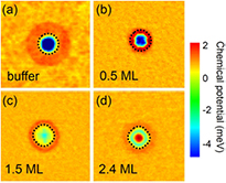
Figure 4. Calculated 2D SCP distribution for nanoholes with a period of 2 µm at various growth stages. (a) After Si buffer-layer growth (corresponds to figure 3(a)). (b)–(d) After Ge deposition of 0.5, 1.5 and 2.4 MLs, respectively. (Corresponding to figures 3(b)–(d), respectively). Image size: 850 × 850 nm2. The black dash lines indicate the boundary of the nanoholes.
Download figure:
Standard image High-resolution imageIn order to verify the validity of the kinetical model above for the QD ordering at large periods, we have grown a series of samples with varying pattern periods and nanohole diameters (D) at a Ge overdose growth regime (i.e. secondary dots on flat regions were formed), and we try to track the Ge adatoms' surface diffusion statistically via counting the secondary dot areal density. Figures 5(a)–(f) show the AFM images of the low-density ordered QD samples grown by depositing Ge of 6 MLs at 450–550 °C and 550–600 °C, respectively. A and B in figure 5(c) mark a square region around one nanohole and a square region with 4 nanoholes as vertexes, respectively. Both square regions have the same area of P2. NA and NB are the secondary dot areal density in regions A and B, respectively. The ratio of NB/NA as a function of P and D shown in figure 5(g) (NB and NA were the averaged values on six separate regions in each sample). It was found that NB/NA shows a value larger than 1 for all the samples and increases with both P and D. These results suggest that the Ge adatoms located in close proximity to the nanoholes exhibited a higher probability of being incorporated into the nanoholes than those located far away from them, as schematically illustrated in figure 5(h). This means that the Ge adatoms tend to move to the nanoholes and accumulate therein. This phenomenon is naturally attributed to a lower SCP in the nanohole. It is this lower SCP that causes the initial nucleation and growth of Ge dots in the nanoholes. In turn, the formation of Ge dots in the nanoholes consumes Ge adatoms around the nanoholes, resulting in a smallar secondary dot areal density around the nanoholes.
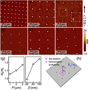
Figure 5. Surface morphology of the Ge QD arrays grown at (a)–(c) 450–550 °C and (d)–(f) 550–600 °C with various periods and nanohole diameters, respectively. (g) The ratio of NB/NA as a function of P and D. (h) Schematic representation for the different probabilities that Ge adatoms exhibit when they are incorporated into the nanoholes.
Download figure:
Standard image High-resolution imageAlthough our growth results demonstrated that low temperature (LT) growth is a robust route to realize ordered Ge QDs with large periods, high-density point defects are often accompanied in the LT epitaxial growth and thus degrade the optical quality of QDs [31]. We have carried out marco-PL measurements for the LT grown low-density ordered Ge QDs with a period of 1 µm (figure 1(b)), and found that a post-growth rapid thermal annealing (RTA) treatment can dramatically enhance their PL intensity. For PL measurements, a 100 nm thick Si layer was capped at 400 °C to suppress the surface non-radiative recombination of excitons. The RTA treatment was carried out at 680 °C for 120 s under the ambience of forming gas. Figure 6(a) shows the marco-PL spectra for both the as-grown and the post-RTA treated samples measured at 15 K under an excitation power density of 1200 mW cm−2. Roughly 500 Ge QDs were excited in the marco-PL measurement. A dramatic enhancement of the PL intensity was observed for the QDs after RTA treatment. Two sub-peaks located at 878 and 921 meV were clearly observed and were attributed to the transverse-optical replica (TOdot) and the non-phonon (NPdot) peaks of the Ge QDs, respectively [32, 33]. A blueshift of ∼110 meV and a slight redshift of ∼4 meV were observed for NPdot and NPWL peak energies, respectively, for the post-RTA treated sample as compared to the as-grown one. Generally, the Si/Ge intermixing during annealing [34] would reduce the Ge content in WL and result in a blueshift for the PL peak energy. However, the intermixing would also lead to a widening for the quantum well of WL, which results in a redshift. There were two opposite effects, so a slight redshift of ∼4 meV was observed. For the QDs with a much higher Ge content, the Si/Ge intermixing during RTA is much more severe and plays a dominant role, thus a large blueshift of 110 meV was observed in the PL peak energy. Moreover, both the NPWL and the Si TO replica (TOSi) intensities were significantly weakened after RTA treatment. Such attenuation is attributed to the enhanced carriers capturing and radiative recombination capability for the QDs after RTA treatment, and indicates an improved QD crystal quality.
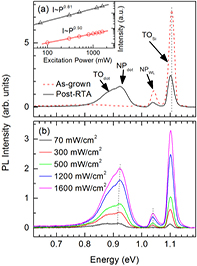
Figure 6. (a) Marco-PL spectra for the as-grown ordered low-density Ge QDs and those after the RTA treatment measured at 15 K under an excitation power density of 1200 mW cm−2. The inset shows the excitation power dependence of the integrated PL intensity for the as-grown and the post-RTA samples, respectively. (b) Excitation power-dependent PL spectra of the post-RTA treated QD sample.
Download figure:
Standard image High-resolution imageThe inset of figure 6(a) shows the power dependence of the integrated PL intensity (I) for both the as-grown and the post-RTA treated samples. The relationship between I and the excitation power (P) (I ∼ Pα) was found to be sublinear with α of 0.5 and 0.81 for the as-grown and the post-RTA treated samples, respectively. The sublinear relationships indicate a typical type-II band alignment of Ge QDs embedded in Si matrix [35]. However, the increase of α from 0.5 to 0.81 for the post-RTA treated sample suggests a significant enhancement of the PL efficiency. Figure 6(b) shows the excitation power dependent PL spectra of the post-RTA treated QD sample. As has already been established, with increasing excitation power, the PL peak energies for Ge QDs should show a large blueshift due to the type-II band bending effect, whereas for Ge WLs the blueshift would be much reduced owing to the type-I band alignment [32]. From figure 6(b), it is clearly seen that the QD peak energies blue-shifted with increasing excitation power while the WL peak energies remained unchanged (as indicated by dash lines), supporting previous attributions of the PL peaks. All of those PL results inform us that by combining the low-temperature MBE growth with post-growth high-temperature RTA treatment, ordered Ge QDs with high optical quality and large periods can be achieved, which are suitable for the Si-based cavity quantum electrodynamics applications.
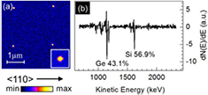
For a full characterization of the low-density ordered Ge QDs inside the nanoholes, SAM was also introduced to determine the Ge surface elemental distribution and the mean Ge content of QDs. Figure 7(a) shows the Ge SAM image acquired on the ordered QD sample shown in figure 1(c) (post-RTA treated). The inset shows a high resolution Ge SAMs image acquired on a single Ge QD inside the nanohole. By carefully examining the contrast on the image, it was found that the mean Ge content on the flat WL region between the nanoholes is far smaller than that in the QDs, and all the QDs have roughly the sane Ge content. Figure 7(b) shows the Auger spectra acquired on the QD site in the inset in figure 7(a). The mean Ge content of QDs in the nanoholes was found to be 43.1% . Such a result coincides approximately with the PL measurement shown in figure 6, from which the mean Ge content in QDs could roughly be estimated to be 53% from the PL peak energy of 921 meV.
Figure 7. (a) 2D Ge SAMs image for the low-density ordered Ge QD sample shown in figure 1(c). The inset shows a high resolution Ge SAMs image acquired on a single Ge QD inside the nanohole. (b) The Auger spectra acquired on the Ge QD site shown in the inset of (a).
Download figure:
Standard image High-resolution image
4. Conclusions
In conclusion, growth of low-density ordered Ge QDs on patterned Si (0 0 1) substrate was investigated. Ordered Ge QDs with different periods were realized, the largest period being 15 µm. The realization of low-density ordered QDs is attributed to a lower SCP inside the nanoholes, which means an immediate nucleation and zero critical thickness for Ge QDs inside the holes. This attribution is evidenced by experimental data, verified by the observation that the Ge adatoms around the nanoholes exhibited a higher probability of being incorporated into the nanoholes. This is supported by calculated results on SCP evolution with growth. It is suggested that ordered Ge QDs with any large periods could be achieved in this scenario. The optical properties of the low-temperature-grown Ge QDs showed a remarkable improvement after a post-growth RTA treatment.
Acknowledgments
This work was supported by special funds for the Major State Basic Research Project (Nos 2011CB925601, 2013CB933303 and 2013CB632104) of China, and the Natural Science Foundation of China (NSFC) under Project Nos 61274016, 10974031 and 61177049. Y J Ma gratefully acknowledges the support of Fudan University, under the Research Support Project for Outstanding PhD Students.