
Abstract
The evolution of resistance switching behaviour of an Ag/DyMnO3/Ag/DyMnO3/Pt memristor structure under repetitive voltage sweeping is investigated. It is observed that the current–voltage (I–V) characteristic evolves from simple bipolar switching behaviour to a complicated switching sequence, which is applicable in passive crossbar arrays. It is suggested that the filament morphology can be modulated by accumulation and release of the Joule heating and Ag ions/atoms residing inside the DyMnO3 layer during continuous switching. The filament growth/dissolution near the upper surface of the middle Ag layer plays a key role in the consequent I–V characteristics.
Export citation and abstract BibTeX RIS
Resistance random access memory (RRAM) has attracted increasing attention due to its high speed, low power consumption and higher density. It has become one of the most promising candidates for next-generation nonvolatile data storage [1, 2]. Recently, remarkable progress in understanding the physical mechanisms [3–7] and improving the switching performance has been achieved [8–12]. For a RRAM cell composed of an active electrode (e.g. Ag, Cu)/transition-metal oxides/inert electrode (e.g. Pt, Au) sandwiched structure, the bipolar voltages generate/dissolve the active metal filaments inside the oxide layer and give rise to the switching between a nonvolatile high resistance state (HRS) and a low resistance state (LRS), as evidenced by the dynamic observations using transmission electron microscopy [4, 5, 8]. In practical applications, many of such cells are integrated into stacked crossbar arrays to satisfy the demand for high memory density. However, this integration strategy brings out a sneak path problem, in which the HRS of one selected memory cell is possibly misread as the LRS, because there are many other cells parallel to the selected cell, and a considerably large current possibly flows through some of them, generating a sneak current path [13].
To solve this problem, a variety of device concepts and structures have been proposed and investigated recently [12, 14]. One way is to anti-serially connect two identical bipolar cells so that a complementary structure composed of Pt/Ta2O5−x/TaO2−x/Pt/TaO2−x/Ta2O5−x/Pt is developed [2]. The other way is to serially connect a bipolar memory cell with a resistor of high current–voltage (I–V) nonlinearity, such as Pt/TiO2/VO2/Pt structure where VO2 layer acts as such a resistor [15]. The third method is the one transistor and one resistor (1T1R) structure [16]. Using one of these three structures and a special reading and writing/erasing strategy, all unselected cells will be at the HRS and hence the resistance misreading of the selected cell can be avoided [13, 15, 16].
Nevertheless, for many bipolar memory cells, a forming process is usually needed and carried out by applying a voltage with a defined polarity [2, 7, 8]. When these kinds of cells are packaged geometrically in the first way, i.e. anti-serial connection of two bipolar cells, the difficulty lies in the fact that the forming process cannot be carried out through the head and tail electrodes of this geometrical package, because the drops of opposite polar voltages on the two anti-serially connected cells cannot be satisfied at the same time. Hence, the forming operation on the two cells must be performed separately, and it needs the third electrode where the two bipolar cells are anti-serially connected, which complicates the circuit design and operation. For the second package geometry, it is difficult to find a resistor that has very large I–V nonlinearity. Due to these problems cell reliability and power consumption will become important issues. Moreover, the 1T1R structure increases the size of the individual cell from 4F2 to 6F2 and impedes the 3D stacks, wherein F is the smallest lithographically resolvable lateral dimension [16]. In this paper, we develop a continuous switching cycling approach to overcome the sneak path problem in a passive crossbar and demonstrate it in a memristor composed of Ag/DyMnO3/Ag/DyMnO3/Pt structure. The reason to choose DyMnO3 lies in the fact that it is multiferroic with a proper band gap for electrically driven resistive switching [17–19]. During continuous switching cycles, the I–V characteristic of the anti-serially packaged cell evolves from the simple bipolar behaviour to a complicated one that suits for application in passive crossbar arrays. In this method, continuous switching is performed through the head and tail electrodes of the anti-serially packaged cell, and no other circuit design/operation is needed for the crossbar application.
In our experiment, we deposited a 240 nm-thick DyMnO3 film on a (1 1 1) Pt/Ti/SiO2/Si substrate using pulsed laser deposition (PLD), with a laser energy density of 3.0 J cm−2 and a repetition rate of 3 Hz. The deposition temperature and oxygen ambient pressure were ∼850 °C and 15 Pa, respectively. The as-grown film was then in situ annealed at the same temperature for ∼10 min in an oxygen ambient of 100 Pa. After the sample was cooled down to room temperature, a 100 nm-thick Ag film was deposited on the DyMnO3 film using ion sputtering. Again, another DyMnO3 layer was deposited on the Ag surface by PLD with the same conditions as the earlier one. Finally, Ag top electrodes with size of ∼100 µm in diameter were deposited by ion sputtering with a shadow mask at room temperature.
The scanning electron microscopy (SEM) image depicts the cross-sectional profile of the DyMnO3/Ag/DyMnO3/Pt structure, as shown in figure 1(a). The large grain size of DyMnO3 and the rough interfaces would benefit depressing the randomicity of the filament's distribution and enhance the switching uniformity [20]. The x-ray diffraction pattern shows that the DyMnO3 films are polycrystalline. To measure the electrical properties of this cell, a voltage was applied on the Ag top electrode and the Pt bottom electrode was ground, as schematically depicted in figure 1(b). The I–V characteristics were measured by the two-probe method using a Keithley 2636A source-measure unit, in which the voltage sweeping was performed in the pulse stair mode with a pulse width of 0.1 ms and a pulse separation of 1 ms.
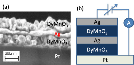
Figure 1. (a) Cross-section SEM image of the DyMnO3/Ag/DyMnO3/Pt structure. (b) A schematic configuration of the Ag/DyMnO3/Ag/DyMnO3/Pt device.
Download figure:
Standard imageThe fresh cell is usually in the HRS with resistance ∼105 Ω, and no special forming process for activating the bipolar resistive switching is needed. Figure 2(a) demonstrates the typical bipolar switching of the fresh cell, marked as A-type I–V characteristic. For a positive voltage sweep (0 → 2 V) with a compliance current of 17 mA, the cell was set from the HRS to the LRS at set voltage Vset ∼ 0.3 V. Afterwards, another negative voltage sweep (0 → −1.8 V) causes the cell to reset back to the HRS at reset voltage Vreset ∼ −0.35 V. Recent observations confirmed that bipolar switching in Ag/oxide electrolyte/Pt structure originates from the growth/dissolution of Ag filaments inside the oxide electrolyte near the Pt electrode [21]. Voltages on an active Ag electrode lead to local redox reactions and/or migrations of Ag ions/atoms inside the DyMnO3 layer [5]. It is believed that a similar mechanism takes place in the current cell. The switching from the HRS to the LRS at ∼0.3 V indicates the connection of Ag filaments near the Pt electrode. As a subsequent negative voltage sweep is applied on the Ag electrode, the redox reaction near the Pt electrode and the migration of Ag ions/atoms away from the Pt electrode rupture the connected filaments at ∼−0.35 V, switching the cell back to the HRS.
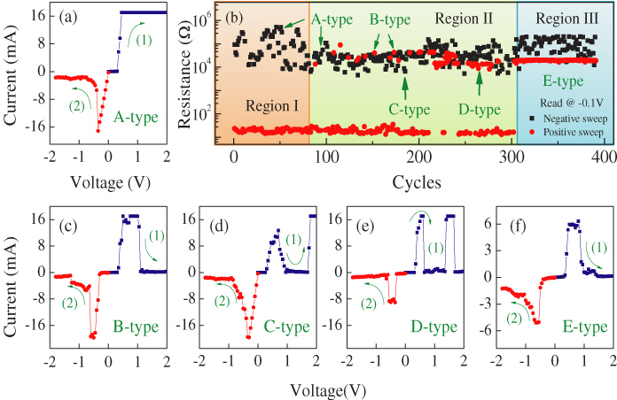
Figure 2. (a) A-type I–V characteristics of the memory cell, with a compliance current of 17 mA. (b) Endurance characteristics of the cell, read out at −0.1 V after the negative or positive voltage sweeps. It is divided into three regions according to the different types of I–V characteristics. In region I, only A-type I–V characteristic is shown. In region II, A-, B-, C- and D-type I–V characteristics appear stochastically. In region III, only E-type I–V characteristic is observed. (c) B-type, (d) C-type, (e) D-type and (f) E-type of I–V characteristics of the cell.
Download figure:
Standard imageBy repeating the above two voltage sweeps in turns, we obtain the switching endurance of the cell, as shown in figure 2(b). The HRS and LRS are read by a voltage of −0.1 V. During the initial several tens of switching cycles (region I), the HRS/LRS ratio is larger than 1000, and the A-type I–V characteristic remains unchanged. Upon further increase in switching cycles (>85 and <300, region II), however, a series of different I–V characteristics including A-, B-, C- and D-types are displayed randomly. Figures 2(c), (d) and (e) show the B-, C- and D-type I–V characteristics, respectively. Their common features are that a voltage of ∼0.3 V switches the cell to the LRS and a sufficiently large negative voltage (< −0.6 V) maintains or switches the cell to the HRS, consistent with the switching mechanisms mentioned above. When the switching cycle is larger than 300 (region III), A-, B-, C- and D-type I–V characteristics can no longer be observed and instead only E-type I–V characteristic is observed, as shown in figure 2(f). E-type and B-type I–V characteristics have similar switching behaviour except for the compliance-free characteristic in E-type (the maximum current in E-type I–V is below the compliance current setting).
For B-, D- and E-type I–V characteristics, the cell undergoes switching from one HRS to the LRS and finally back to another different HRS during the positive/negative voltage sweep. To verify the different natures of the two HRSs, two continuous positive voltage sweeps are performed. In figure 3(a), the LRS (∼100 Ω) in the middle voltage range (0.3 → 0.9 V) appears in the first sweep but is absent in the second sweep, indicating that the positive voltage can switch only the first HRS (HRS1, ∼2 × 10⁴ Ω) to the LRS. Hence, this demonstrates that the second HRS (HRS2, ∼105 Ω) has a different nature from HRS1. The positive sweep results in the switching sequence HRS1 → LRS → HRS2. Similarly, the negative sweep (0 → −1.8 V) causes the reverse switching with the sequence HRS2 → LRS → HRS1. Such switching sequences demonstrate the two different nonvolatile HRSs, which can be written/erased by sufficiently large positive/negative voltage pulses.

Figure 3. I–V characteristics of two continuous positive voltage sweeps from 0 to 2 V.
Download figure:
Standard imageIf such cells are integrated into passive crossbar arrays, the E-type I–V characteristic provides a good solution to the sneak path problem. For single cell, the switching from HRS1 to HRS2 is performed by a positive voltage (>1.5 V), while the opposite switching from HRS2 to HRS1 is operated by a negative voltage (< −1.5 V). Resistance states of the cell can be read by a voltage Vread (0.4 V < Vread < 0.8 V). According to the E-type I–V characteristic, such Vread does not change HRS2 but can switch HRS1 to the LRS. Hence, with this Vread, a low current level signal (<0.03 mA) shows HRS2, while a large current level signal (>3 mA, i.e. LRS) indicates that it is HRS1 before the reading operation. Due to the destructive readout of HRS1, HRS1 needs to be rewritten by a negative voltage pulse after the reading operation. These results can be transferred directly to passive crossbar arrays. Considering that a sneak current is flowing through three serially connected cells (the shortest and simplest sneak current path), the voltage drop on each serially connected cell is only ∼Vread/3 [13], smaller than 0.3 V. Based on the E-type I–V characteristic, all cells in the crossbar arrays at ∼ ± Vread/3 are high resistance, which prevents the sneak current paths.
An interesting fact is that a voltage of ∼−0.35 V allows the cell to suffer opposite switching processes among the different I–V behaviours, as re-shown in figure 3(b). In the A- and C-type I–V curves, the voltage of ∼−0.35 V causes the LRS → HRS1 switching, while in the B-, D- and E-type I–V curves, the voltage of ∼−0.35 V causes an opposite switching (from HRS2 to LRS). It is noted that the resistance of Ag/DyMnO3/Pt is in the LRS as the whole cell of Ag/DyMnO3/Ag/DyMnO3/Pt is set to HRS2. This fact indicates that the rupture of the filament inside Ag/DyMnO3/Ag causes the appearance of HRS2. According to the forming mechanism of cylindrical Ag filaments in the oxide electrolyte [5], except for the region near the Pt electrode, the local region near the upper surface of the middle Ag layer is another narrow link of filaments, as illustrated in figure 4(b). The sufficiently high Joule heating may likely rupture the filament in this narrow region, as illustrated in figure 4(c).
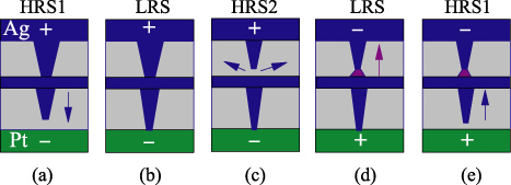
Figure 4. Illustrations of growth/dissolution of Ag filament during the voltage sweeps. The arrow indicates the migration direction of Ag ions/atoms. (a) to (f) in sequence illustrate the switching processes of HRS1 → LRS → HRS2 → LRS → HRS1 in B- or E-type I–V curves.
Download figure:
Standard imageGiven this understanding of the origin of HRS2, not only can the HRS2 → LRS switching by a voltage of −0.35 V be well understood, but also the B- or E-type I–V behaviour, as schematically shown in figures 4(a)–(e). First, a positive voltage (∼0.3 V) causes the switching from HRS1 (figure 4(a)) to the LRS (figure 4(b)) due to the connection of Ag filaments towards the Pt electrode. Then a further increase in the positive voltage generates considerable Joule heating near the upper surface of the middle Ag layer, and as a result dissolves the filaments there and switches the LRS to HRS2 (figure 4(c)). Subsequently, a negative voltage (∼−0.35 V) helps the Ag atoms to migrate from the middle Ag layer towards the top Ag electrode and recaptures the filaments, leading to the HRS2 → LRS switching (figure 4(d)). Finally, a further increase in negative voltage (< −0.6 V) helps the Ag atoms to migrate away from the Pt electrode, switching the LRS back to HRS1 (figure 4(e)) again. Naturally, if HRS2 does not appear after the positive voltage sweep (e.g. the A-type I–V), the LRS → HRS1 switching at ∼−0.35 V will happen.
With the continuous switching cycle, the accumulative Joule heating and increasing residual Ag ions/atoms inside the DyMnO3 layer would modulate the filament morphology [5], allowing for a possibility to rupture the filaments near the upper surface of the middle Ag layer by the Joule heating and to reach the HRS2. With this argument, the stochastic appearance of the A-, B-, C- and D-type I–V behaviour in region II and only the E-type I–V behaviour in region III in figure 2(b) can also be well understood. In region II, the positive voltage induced growth and the accumulated Joule heating induced dissolutions of the Ag filaments co-occur and compete with each other, giving rise to big fluctuations in the filament morphology. Hence, during the voltage sweep of 0 → 2 V, except for the HRS1 → LRS switching (A-type) and HRS1 → LRS → HRS2 switching (B-type), repetitive switching between the HRS and the LRS, such as HRS1 → LRS → HRS2 → LRS (C-type) and HRS1 → LRS → HRS2 → LRS → HRS2 (D-type), is possible. As the cycle proceeds, however, the residual of Ag ions/atoms inside DyMnO3 and the accumulation and release of the Joule heating would reach a balance, resulting in a relatively stable filament morphology. This may be one of the reasons for the appearance of the E-type switching at the end.
To verify the accumulating effect of the Joule heating during repetitive switching, we also carried out 500 resistive switching cycles on other fresh cells, using the same sweeping scheme but with different compliance currents. A larger compliance current means more Joule heating generated and released into DyMnO3. Our experiments revealed that similar evolutions from the A- to E-type I–V behaviour are also available as the compliance current is reduced from 17 to 0.7 mA. We count the probability for the B-type I–V events over the whole 500 switching cycles and the data are plotted in figure 5(a). Clearly, the probability increases dramatically with the compliance current, demonstrating that the sufficiently large Joule heating benefits the appearance of the B-type I–V characteristic. That is to say, the accumulated Joule heating during the cycle accelerates the evolution of the switching behaviour. Moreover, figure 5(b) shows the B-type I–V curves with different compliance currents of 0.7, 3 and 17 mA. As the compliance current is reduced from 17 to 0.7 mA, the voltage range, in which the current remains at the compliance level (corresponds to the LRS), is increased from 1.05–0.35 = 0.7 V to 1.95–0.45 = 1.5 V. This fact also verifies the important role of Joule heating during resistive switching. A low compliance current means a restriction of the heating power, and as a result a long heating time (equal to a high voltage range here) is needed to produce comparative heat.
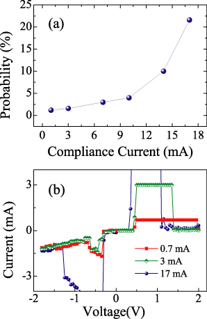
Figure 5. (a) Compliance current dependent probability of B-type I–V characteristic appearing over 500 consecutive switching cycles. (b) Typical I–V characteristics of the memory cell, with compliance currents of 0.7 mA, 3 mA and 17 mA, respectively.
Download figure:
Standard imageBased on the above discussion, it is understood that the evolution of I–V characteristics depends mainly on the migration of Ag ions/atoms and the evolution of the residual Ag ion/atom inside the matrix of DyMnO3, while DyMnO3 is not directly involved in the resistance switching. Therefore, we believe that the replacement of DyMnO3 by different material systems, such as titanium oxide and tantalum oxide based systems, may bring out similar E-type I–V behaviour after many switching cycles. It needs to be addressed that the evolution of Ag filament inside transition metal oxide has some randomness, which would affect the stability of the E-type I–V characteristic. Further optimization of our method is definitely needed.
In addition, the result of figure 5 also implies that the training process, i.e. the switching of many cycles, could be directly performed on the newly fabricated crossbar arrays. First, this training process uses the voltage control mode, and the sneak current path cannot alter the voltage drop on the addressed cell. Second, the sneak current path would reduce the actual current flowing through the addressed cell if current compliance controlling takes effect. In other words, the sneak current path just plays a role in reducing the actual compliance current. In fact, as indicated in figure 5, the reduction of the compliance current from 17 to 0.7 mA cannot suppress the appearance of the E-type I–V characteristic after many continuous switching cycles. Hence, the training out of the E-type I–V characteristic can also be realized on the newly fabricated crossbar arrays even though there are sneak current paths.
In summary, we have observed the evolution of the I–V characteristics from A- to E-type under continuous switching cycle training in the Ag/DyMnO3/Ag/DyMnO3/Pt structure. The A-type I–V curve displays a simple bipolar resistive switching, while the E-type I–V curve demonstrates the switching between two different nonvolatile HRSs during the positive/negative voltage sweeps. E-type I–V behaviour can be used to avoid the sneak path problem and is suitable for the application in passive crossbar arrays. It is suggested that during continuous cycling, the accumulation and release of the Joule heating and the residual of Ag ions/atoms inside DyMnO3 determine the filament morphology, and eventually the growth/dissolution of the filaments near the upper surface of the middle Ag layer plays a key role in the E-type I–V characteristics.
Acknowledgments
This work was supported by the National 973 Projects of China (Grant Nos 2011CB922101 and 2009CB623303), the Natural Science Foundation of China (Grant Nos 11074113 and 11234005), the China Postdoctoral Science Foundation (Grant No 2011M500119) and the Priority Academic Program Development of Jiangsu Higher Education Institutions, China.