
Abstract
Charge-coupled devices (CCDs) have been the most common visible and nearultraviolet imaging sensors in astronomy since the 1980s. Almost all major astronomical instrumentation utilizes CCD imagers for both scientific observations and the more routine tasks such as telescope guiding. In this short review, we provide a brief history of CCDs in astronomy and then describe their operation as they are most commonly implemented for scientific imaging. We discuss specialized CCD sensors which have been developed and effectively utilized in modern astronomical instrumentation. We conclude with an overview of the characterization of CCDs as performed in detector laboratories and at telescopes and discuss anticipated future advances.
Export citation and abstract BibTeX RIS
1. Introduction
Charge-coupled devices (CCDs) have been the most common visible and near-ultraviolet imaging sensors in astronomy since the 1980s. Almost all major astronomical instrumentation utilizes CCD imagers for both scientific observations and the more routine tasks such as telescope guiding. While modern silicon processing techniques have allowed great advances in Complementary Metal Oxide Semiconductor (CMOS) imager capabilities, the CCD's outstanding low light level performance has allowed it to remain the detector of choice for not only current generation instruments but also those being planned for the next decade.
In this review, we provide a brief history of CCDs in astronomy and then describe their operation as they are most commonly implemented for scientific imaging. We next discuss specialized CCD sensors that have been developed and effectively utilized in modern astronomical instrumentation. We conclude with an overview of the characterization of CCDs as performed in detector laboratories and at telescopes and discuss anticipated future advances.
2. Brief History of CCDs in Astronomy
The CCD was invented by Bell Telephone Laboratories researchers Willard S. Boyle and George E. Smith in late 1969 and first described in 1970 (Boyle & Smith 1970; Amelio, Tompsett & Smith 1970). The new detector was recognized almost immediately after its invention for its scientific imaging potential. Among the earliest astronomical applications of a CCD for ground-based observing was in 1976 at the University of Arizona (Smith 1976). "Solid State Imaging" developed rapidly in the 1970s and beyond as a replacement for photographic techniques. Further developments of the CCD would lead to increased quantum efficiency and image format (size and pixel count), reduced noise, and improved cosmetics. By the 1980s, it was clear that CCDs would be the sensor of choice for future astronomical imaging. An interesting review of the history of CCDs and their early use in astronomy is given in "Scientific Charge-Coupled Devices" by Janesick (2001).
Continued developments from the 1980s to the present have led to devices with over 100 million pixels, read noise as low as one electron, quantum efficiency near 100%, and useful sensitivity from the X-ray through near-IR. While CCDs are losing favor to CMOS imagers for commercial imaging applications, they are still state-of-the-art sensors for astronomical imaging due to their size, efficiency, and low noise. It is likely that CMOS imagers will continue to improve and eventually replace CCDs in astronomy, especially as the number of fabrication facilities in which CCDs can be manufactured decreases worldwide. However, there are still significant advances in CCD technology every year as scientists and engineers develop ever more demanding applications for sensors in the instrumentation needed for the next generation of very large telescopes.
3. CCD Operation
3.1. Architectures
A charge-coupled device (CCD) is an imaging detector which consists of an array of pixels that produce potential wells from applied clock signals to store and transport charge packets. For most CCDs, these charge packets are made up of electrons which are generated by the photoelectric effect from incident photons or from internal dark signal. Gate structures on the silicon surface define these pixels in one direction, while electrical potentials from implants typically define the pixels in the orthogonal direction. A time-variable voltage sequence is applied to these gates in a specific pattern which physically shifts the charge to an output amplifier which acts as a charge to voltage converter. External electronics (and often a computer) convert the output sequence of voltages into a two-dimensional digital image.
Pixels are composed of phases which each have an electrical connection to the externally applied voltage sequence. Each phase acts much like a metal oxide semiconductor (MOS) capacitor. The array of pixels in each direction (rows or columns) has a repeating structure of these phases in which each phase of the same name has the same applied voltage or clock signal. See Figure 1 for a schematic representation of a simple three-phase CCD. There are two, three, and four phase CCDs in fairly common use, although single phase devices also exist. As an example, a three-phase device needs three different electrical connections for shifting in each direction (x/y, columns/rows, or parallel /serial), for a total of six applied clock signals. The distance from one potential minimum to the next defines the resolution of the detector, and is the pixel pitch. A three-phase CCD therefore has phases spaced 1/3 of the pixel size apart. Typical CCD pixel sizes used in astronomy are 9–30 μm.
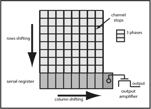
Fig. 1. Physical layout of a typical three-phase CCD.
CCDs can be divided into several types, including linear, area, frame transfer, and interline transfer. A full-frame CCD uses the entire area (all pixels) to collect light. This is the optimal use of silicon area and the most common detector used in astronomy. These detectors require a camera shutter to close during readout so that electrons are not generated when charge is transferred which would result in image streaking.
A frame store CCD has half of the pixels covered with an opaque mask (frame store area) and half of the pixels open to incident light (image store) which collect photons during integration. This allows a very rapid shift (microseconds) from image store to frame store after integration. If the shift is fast enough and the incident light is not too bright, there will be no image streaking and no external shutter is required. Often telescope guide sensors (used to correct for tracking errors as a telescope moves) are frame transfer devices which eliminate the need for a high-speed mechanical shutter. See Theuwissen (1995) for a good description of CCD sensor architectures and operation.
3.2. Clocking
During integration (or light collection), the potential minimums are defined to collect electrons when a positive voltage is applied to one or two phases. The adjacent phases must be more negative to create a barrier to charge spreading or image smear will occur. No shifting occurs during integration, only photoelectrons are collected. Typically, a device must be cooled if integration is more than a few seconds or self-generated dark current will fill the potential wells and photogenerated signal will be lost in the associated noise. Channel stops (along columns) are created with implants during fabrication to keep charge from spreading between adjacent columns.
Charge packets collected in the potential well minima are shifted when the minima (for electrons) are moved from under one gate to under the adjacent gate. This is performed by applying a voltage sequence to the phases to shift one row at a time toward the serial register. There may be multiple image sections on a device and so some charge packets may move in different directions toward their respective output amplifier.
There is one serial (horizontal) register for each output amplifier and it receives charge from the associated columns. All charge is transferred from the last row of an image section to the serial register one row at a time. The serial register then shifts charge out to the amplifier at its end in the same manner used for shifting charge along columns. Serial registers may be split so that charge from one half moves in one direction to an output amplifier and charge from the other half moves toward an opposite end amplifier. Serial registers may even have multiple taps (output amplifiers) distributed along their length for high frame rate operation.
The voltage timing pattern may be changed, so charge from multiple pixels is combined together during transfer to the serial register (parallel binning) or to the output amplifier (serial binning). This decreases the spatial resolution of the detector by creating larger effective pixels which in turn allows higher charge capacity and therefore larger dynamic range. It also allows increased read-out speed (higher frame rate) since every pixel is not individually sampled at the output amplifier which takes a significant amount of time. Binning is also called "noiseless co-addition" since summing comes before readout, when read noise is generated. Many cameras can be configured to vary binning in real time to optimize performance under various imaging conditions.
3.3. Charge Sensing
The photogenerated electrons are shifted off the end of the serial register to the output amplifier where the charge is sensed and an output voltage is produced. The charge to voltage conversion occurs because of the capacitance of the output node according to the equation V = Nq/C where C is the capacitance of the node (typically of order 10-13 F), N is the number of electrons on the node, and q is the electronic charge (1.6 × 10⁻¹⁹ C). Typically a single electron produces from 1 to 50 μV at output depending on C. This voltage is buffered by the output amplifier to create a measurable voltage, usually across a load resistor located off the CCD as part of the camera controller. This output voltage is easily amplified in the controller and converted to a digital signal by an analog-to-digital converter to form a digital image. The node must be reset before each pixel is read so that charge does not accumulate from all pixels. This is accomplished with a separate "reset" transistor.
3.4. Illumination (Front vs. Back)
CCDs are often categorized as being either front-illuminated or back-illuminated devices. This term indicates whether light from the imaged scene is incident on the front side of the detector (where the pixel structures and amplifiers are located) or the opposite or backside (see Fig. 2).
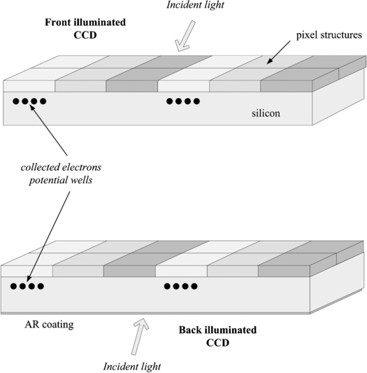
Fig. 2. Two illumination modes of a CCD. A frontside detector is illuminated through the structures which define the pixels. A backside detector is illuminated directly into the silicon on the opposite (back) side as a frontside device.
Front-illuminated CCDs have photons incident on the gate structure or "frontside." They are the least expensive devices since they are used directly as fabricated on the silicon wafer with no additional processing steps. However, the frontside gates absorb almost all blue and UV light and so frontside devices are not directly useful for imaging at wavelengths shorter than about 400 nm. In addition, the physical gate structure causes reflections and complex quantum efficiency (QE) variations with wavelength due to interference between material layers (oxides/nitrides and polysilicon). There are several techniques to improve front-illuminated device performance, including using fairly transparent indium tin oxide (ITO) and thin polysilicon gates, using microlenses deposited on every pixel, and applying scintillators or other wavelength conversion coatings to the CCD frontside. However, it is most common for astronomical detectors to be used in the "back-illuminated" mode rather than utilize these less-efficient frontside techniques.
Back-illuminated devices require additional postfabricated steps, sometimes called thinning. Compared to front-illuminated devices, they are much more efficient in sensing light because the incident photons impinge directly into the photosensitive silicon material. For many high-performance imaging applications, back-illuminated CCDs are the clear detector of choice even with their higher cost. QE is limited only by reflection at the back surface and the ability of silicon to absorb photons, which is a function of wavelength, device thickness, and operating temperature. An antireflection-coated back-illuminated CCD may have a peak QE > 98% in the visible. Back-illuminated sensors may have response throughout the X-ray and UV spectral regions as well. While optical absorption and most multiple reflections inside the frontside structures are avoided with backside devices, they do suffer from "interference fringing" due to multiple reflections within the thin silicon itself. In recent years, many back-illuminated devices have been made much thicker than previously possible to increase absorption in the red as well as to decrease the amplitude of fringing. Appropriate antireflection coatings on the backside also contribute to reduced interference fringing.
4. CCDs for Astronomy
Many CCDs have been developed over the years which are of special interest to scientists building astronomical instrumentation. Because there are specific requirements for astronomical imaging which are not critical in most commercial imaging applications, astronomers have often made custom CCD sensors for their observational needs. A brief comparison of astronomical verses versus commercial drivers is given below.
- 1.Pixel size: Astronomical sensors use relatively large pixels for large full-well capacity and dynamic range while commercial devices utilize small pixels in order to use smaller, less-expensive sensors.
- 2.Dark current: Astronomical sensors require very low dark signal because they are used for long, photon-limited integrations. Cooling to -100°C or colder is often required. Commercial systems are typically used at room temperature which allows for much less-expensive cameras.
- 3.Read noise and frame rate: Astronomical sensors usually require total system noise of just a few electrons and therefore are read out at very slow speeds. Most commercial applications require a much higher frame rate due to motion capture requirements and the high ambient light levels allow for higher system noise.
- 4.Quantum efficiency: Astronomical sensors typically need near 100% efficiency over wide spectral range because they are used in photon-limited applications. Commercial sensors typically require much lower sensitivity and only over the human eye's spectral response region (visible light).
These requirements have led to the development of large format, back-illuminated CCDs which are packaged in a manner compatible with cryogenic cooling. Currently, the largest CCDs have around 100 million pixels and are fabricated as one sensor on a 150 mm silicon wafer (Zacharias et al. 2007; Jorden et al. 2014). Astronomical sensors often have critical flatness requirements to maintain focus in a fast optical beam (Kahn et al. 2010). Mosaics of multiple CCDs are also common in astronomy in order to adequately sample the large focal plane often found on large telescope instruments (Tonry et al. 2006).
4.1. Backside-Illuminated CCDs
The back-illuminated CCD described above must be relatively thin in order for photogenerated electrons to diffuse to the frontside pixel wells and be collected under the sites where they were created. Most CCDs are built on epitaxial silicon with thickness layers which are 10–20 μm thick. The device must be etched down to this thickness range so that the photogenerated electrons are absorbed and detected in this high-quality epitaxial layer. This thinning process is difficult and expensive, leading to the much higher cost of backside sensors. Considerable effort (and funding) across both the space- and ground-based astronomical communities has gone into backside processing techniques since the first backside devices were developed in the 1970s. Optimizations include thinning techniques, the critical backside charging steps, increases in device thickness, and well-tuned antireflection coatings to match scientific requirements.
After a CCD is thinned, it requires an additional step to eliminate what is known as the backside potential well which will trap photogenerated electrons and cause an uncharged device to have lower QE than a front-illuminated device. This backside well is caused by positive charge at the freshly thinned surface where the silicon crystal lattice has been disrupted and therefore has dangling bonds. The backside native silicon oxide also contains positive charge which adds to the backside well. This positive charge traps the electrons at the backside so that they are not detected in the frontside potential wells. Adding a negative charge to the back surface is called backside charging and leads to very high QE, especially when combined with AR coatings (see Fig. 3). Several different techniques have been used to produce high QE with backside devices, depending on manufacturing preferences. They can be divided into two classes, surface charging and internal charging. Surface charging includes Chemisorption Charging (Lesser & Iyer 1998), flash gates, and UV flooding (Janesick 2001; Leach & Lesser 1987). Internal charging includes implant/annealing (doping) and molecular beam epitaxy (Nikzad et al. 1994) and is more commonly used as it can be performed with standard wafer processing equipment.
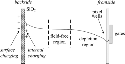
Fig. 3. An internal electrical schematic of a CCD. Positive charge is added near the backside surface to create an electric field which drives electrons to the front side for detection. With no positive charge, the native negative charges at the back surface will create a backside potential well which traps electrons.
When light is incident on the CCD backside, some fraction of it reflects off the surface. This reflectance can be reduced with the application of antireflection (AR) coatings. These coatings comprise a thin film stack of materials applied to the detector surface to decrease reflectance. Coating materials should have proper indices and be nonabsorbing in the spectral region of interest (Lesser 1993, 1987). With absorbing substrates which have indices with strong wavelength dependence (like silicon), thin film modeling programs are required to calculate reflectance. The designer must consider average over incoming beam (f/ ratio) and angle of incidence due to the angular dependence of reflectance.
4.2. Fully Depleted CCDs
Because of the rich astrophysical information which can be obtained from near-IR observations, there is a strong interest in CCD imaging at wavelengths as long as the silicon band-gap limit of about 1.1 μm. Ideally, silicon CCDs used in this spectral region would be as thick as possible to absorb the most red light and to avoid interference fringing (multiple reflections between the front and back surfaces of the sensor). Pioneering work at the University of California's Lawrence Berkeley Laboratory has focused on the development of thick, high silicon resistivity, back-illuminated p-channel CCDs for high-performance imaging (Holland et al. 2003). Today, several commercial manufacturers also make fully depleted relatively thick backside CCDs.
For thick devices, the depletion region where electrons are swept to the potential well minima may not extend throughout the entire device. Photogenerated electrons can diffuse in all directions when there is no electric field in this region, reducing spatial resolution through charge spreading. It is important to minimize the "field-free" region as much as possible or the Modulation Transfer Function (MTF) is greatly reduced. This can be accomplished by increasing the resistivity of the silicon so that the depletion edge extends deeper into the device and by thinning the device as much as possible. Thick CCDs designed to have extended red response should always be fabricated on high-resistivity silicon, typically >1000 Ω-cm, and often have an applied internal electric field derived from potential differences as high as several hundred volts.
4.3. Orthogonal Transfer CCDs and Arrays
An Orthogonal Transfer CCD (OTCCD) has its channel stops replaced with an actively clocked phases, so charge shifting in both directions (along rows and columns) may be achieved. If centroiding of a moving object in the scene is performed with another detector, the feedback can be used to clock the OTCCD in any direction to minimize image blurring. This is a useful function especially when making astronomical observations in which atmosphere motion (scintillation) blurs images. OTCCDs are therefore most useful for high-resolution imaging, eliminating the need for tip/tilt mirrors and their associated optical losses which are more typically used to redirect the optical beam based on a feedback signal.
The Orthogonal Transfer Array (OTA) is a monolithic device composed of (nearly) independent cells which are each an Orthogonal Transfer CCD (Burke et al. 2004). The advantage of the OTA over the OTCCD is that the same detector can both provide the feedback signal and perform the data observation. OTA detectors eliminate the need for a steerable mirror by moving the electronic charge centroid from the image on the detector in the same manner as optically nearby guide stars are measured to move. OTAs have on-chip logic to address the OTCCD cells so that each cell can have independent timing. This allows some cells to be reading out while others are integrating. The integrating cells can be shifting small amounts in X and Y based on the feedback signal obtained from the cells being read out at a higher frame rate. A common observing mode is therefore to read a few cells at high speed and measure the centroid of guide stars. These centroids are then used to provide a feedback signal to shift the integrating cells which are observing objects of scientific interest. OTCCDs and OTAs were developed by Burke and Tonry at MIT/LL and the University of Hawaii (Tonry et al. 1997).
4.4. Electron-Multiplying CCDs
Some astronomical applications require high frame rate imaging at very low signal levels such as wavefront sensing for adaptive optics systems (Gach et al. 2014). Because traditional CCDs have increased read noise when the read-out speed is increased, the Electron-Multiplying CCDs have been developed. These devices have internal gain which is developed in an extended serial register with a very high electric field within each extended pixel (Jerram et al. 2001; Hynecek 2001). As the CCD shifts charge through this extended register, a small avalanche gain (1.01) is achieved. After ∼100 gain stages, an electron packet larger than the read noise is generated and photon counting in low light level conditions is possible. There is noise associated with the gain process and so the expected signal-to-noise ratio must be carefully understood. But for low light level applications with high-speed frame rate requirements these internal gain sensors are often the detectors of choice.
5. Characterization
There are several fundamental sensor characterization techniques which are used to measure CCDs for astronomical observations. While many of these are used in the laboratory when setting up a camera for a particular instrument, they can (and should) also be used to verify performance at the telescope. We briefly describe the major characterization techniques here. Much more detail can be found in the various texts on CCD devices and their uses (Janesick 2001; Theuwissen 1995; McLean 2008).
5.1. Photon Transfer and Full Well
The full-well capacity of a pixel is the maximum number of electrons which a pixel can hold. It is determined by the pixel size and structure, the output amplifier, and the controller electronics. Pixel capacity is a function of area, so bigger pixels (or binned pixels) usually hold more charge and therefore have higher full-well capacity. Full well is often measured by making a Photon Transfer Curve (PTC) plotting log noise (in Digital Numbers or DN) versus log signal (DN). A typical PTC is shown in Figure 4. The system gain constant (electrons per DN) is a critical parameter of an imaging system and is often measured from the photon transfer curve. This constant may be determined from photon statistics by analyzing two flat field images which are used to remove fixed pattern noise. See Janesick (2007) for extensive discussion and examples of photo transfer techniques.
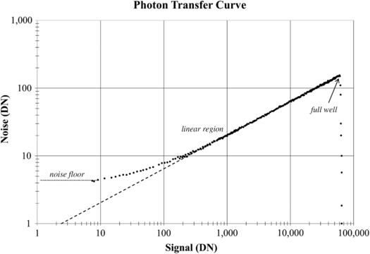
Fig. 4. A typical Photon Transfer Curve used to characterize the output of a CCD.
A linear input signal should produce a linear output signal for a CCD. The difference between the actual and ideal output is the nonlinearity of the system and can be due to silicon defects, amplifier, and/or electronic issues. Linearity is normally characterized by measuring the signal output generated as a function of increasing exposure level. Fitting a line to this data should produce residuals of less than 1% from just above the read noise floor to full well. It is often difficult to deconvolve nonlinearities in the sensor itself from those in the camera electronics and even the system shutter.
5.2. Read Noise
Read noise is the fundamental uncertainty in the output of the CCD. It is often the dominant noise source in a high-performance imaging system. Read noise is typically measured in electrons rms, but is actually a voltage uncertainty. Nearly all high-end cameras use correlated doubled sampling (CDS) to reduce read noise by reducing the uncertainty in absolute charge level at the output node. When the output node is reset, its final value is uncertain due to kTC noise. The CDS technique reduces this uncertainty by sampling each pixel both before and after reset. Before shifting charge from a pixel, the node is reset with the on-chip reset transistor. Its voltage is sampled and recorded. The pixel to be measured is then shifted onto the node. It is again sampled and the difference between the two samples is the actual charge in the pixel. Low-noise MOSFETs with very low capacitance nodes can produce less than two electrons rms read noise with only one (double) sample per pixel.
Read noise is characterized by calculating the standard deviation σ of a zero or bias frame (no light or dark signal). Noise is measured in units of Digital Numbers (DN) from clean subsections of the image and then the system gain constant in (e/DN) is used to find the noise in electrons.
5.3. Charge Transfer Efficiency
Charge transfer efficiency (CTE) is a fundamental imaging parameter specific to CCD systems. It is the efficiency in which charge is shifted from one pixel to the next. Modern CCDs have CTE values of 0.999995 or better. CTE is sometimes temperature-dependent, being worse at low temperatures. CTE is usually calculated by measuring the trailing edge of sharp images or the residual charge after reading the last row or column. An Fe55 X-ray source can also be used in the lab to measure CTE quantitatively. Since each 5.9 keV X-ray produces 1620 electrons and the electron cloud produced is about 1 μm in diameter, each event should appear as a single pixel point source. When CTE is less than perfect, pixels further from the read-out amplifier (for horizontal CTE measurement) or farther from the serial register (for vertical CTE measurements) will be measured to have fewer electrons than closer pixels. By plotting pixel values versus location, one can usually measure CTE to 1 part in 106. When CTE is poor a "fat zero" or preflash, which adds a fixed amount of charge to each pixel before image exposure, may fill traps to improve CTE. There is of course a noise component associated with this added signal.
5.4. Dark Signal
Dark signal (or dark current) is due to thermal charge generation which occurs in silicon and is strongly temperature-dependent (see Janesick [2001]). The usual method of reducing dark current is to cool the detector to -100°C or below with liquid nitrogen. This reduces the dark signal to just a few electrons per pixel per hour. Higher light level measurements often use devices cooled with a thermoelectric cooler to -40°C or warmer. Most commercial CCD systems operate with no cooling and have dark current so high that only limited quantitative measurements are possible.
Often the characterization of dark signal actually includes other signals such as optical glow from diode breakdowns, camera light leaks, and fluorescence. Dark signal characterization is performed by taking multiple exposures and adding them together, usually with a median combine or clipping algorithms to reject cosmic rays. Since dark signal for cooled detectors is of the same order as the device read noise, these measurements are very difficult to make accurately. Spatial variations in dark signal due to clocking artifacts and silicon processing variations can be larger than the mean dark signal values.
5.5. Quantum Efficiency
Quantum efficiency (QE) is the measure of the efficiency with which a CCD detects light. It is one of the most fundamental parameters of image sensor technology and provides the quantitative basis for selecting a frontside or backside device. The absorptive quantum efficiency QEλ is the fraction of incident photons absorbed in the detector and is given by

where Rλ is the reflectance of the detector's incident surface, Ninc is the number of photons incident on the detector surface, Nabs is the number of photons absorbed in the detector, αλ is the wavelength dependent absorption length, and t is the device (silicon) thickness. It can be seen from this equation that QE may be increased by (1) reducing surface reflectance (reduce Rλ with AR coatings), (2) increasing the thickness of absorbing material (increase t), and (3) increasing the absorption coefficient (decrease αλ by material optimization). Because nearly all CCDs are made using silicon, only options (1) and (2) are viable. A variety of measured QE curves are shown in Figure 5.
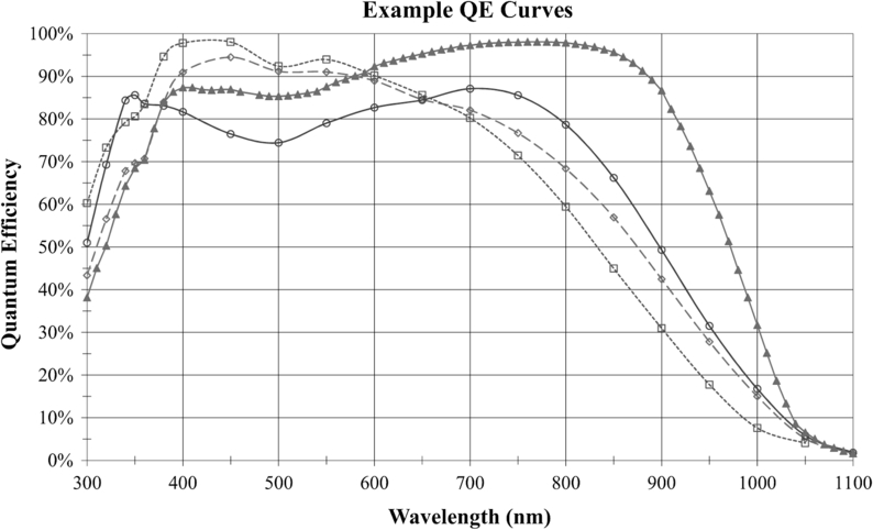
Fig. 5. Typical quantum efficiency curves of backside detectors. The differences in QE are due to the application of different antireflection coatings to each detector as well as device thickness.
Related to QE is Quantum Yield (QY), which is the term applied to the phenomena that one energetic interacting photon may create multiple electrons-hole pairs through collision (impact ionization) of electrons in the conduction band. This can cause the measured QE to appear to be higher than it is, even greater than unity. Since photon energy increases with decreasing wavelength, QY is only important in the UV and shorter spectral regions (< 400 nm).
Characterization of QE is typically performed by illuminating the detector with a known light flux. The actual flux incident upon the sensor is usually measured with a calibrated photodiode having a known responsivity. Ideally, the calibration diode is placed in the same location as the CCD to measure the actual optical beam flux. Errors may be introduced in the measurement when the photodiode and CCD do not have the same spectral response. Because the currents measured are extremely low (nanoamps or less) and color sensitive, the absolute measurement of QE is quite a difficult measurement to make accurately.
6. Future
There are a relatively few manufacturers worldwide who maintain CCD fabrication facilities. CMOS imagers are now used for most imaging applications (cell phones, consumer electronics, etc.) which drive the imaging market much more than the scientific community. However, large pixel image sensors will likely remain CCDs as CMOS pixel sizes continue to shrink. Large pixels are required for most scientific and industrial imaging applications due to their larger dynamic range, although progress continues to improve the full-well capacity of smaller pixels for all image sensors. Very large area scientific CCDs are in demand and continue to grow in size. The simplicity of CCD devices (fewer transistors and other structures compared to CMOS sensors) tends to produce higher yield at very large areas.
Back-illuminated CCDs for high QE and UV and X-ray applications also dominate imaging systems, because backside CMOS processing is currently focused mainly on commercial applications which need very small pixels, and therefore very thin devices, for reasonable MTF. However, backside processing techniques used to make scientific CCDs are currently being applied to CMOS sensors for low-noise and low-light applications. These techniques will no doubt continue to increase the availability of very high-performance CMOS sensors in the future. Similarly, enhanced red response requires relatively thick silicon (>20 μm) and most CMOS processes are optimized for much thinner silicon. The low voltages used on CMOS imagers may limit the depletion depth possible in thick sensors and so enhanced red QE detectors are likely to remain CCDs for some time.