
Abstract
Transparent amorphous oxide semiconductors have unique electron transport properties, such as large electron mobility (10–50 cm2/Vs) and the absence of a Hall voltage sign anomaly, that are not seen in conventional amorphous semiconductors. This class of materials has been attracting much attention as a channel layer in thin-film transistors (TFTs) utilizing the above features along with the processing advantage that thin films can be deposited at low temperatures by conventional sputtering methods. The primary driving force for this trend is a rapidly emerging demand for backplane TFTs that can drive the next generation of flat-panel displays. This article reviews the recent advances in fundamental science of these materials and their TFT applications. Emphasis is placed on the view that high ionicity in chemical bonding and large spherical spread of unoccupied metal s orbitals in p-block metal oxides lead to the realization of electronic structures that are advantageous for n-channel TFT applications. Amorphous oxide semiconductors are compared with conventional hydrogenated amorphous silicon, which is used widely as the channel material for backplane TFTs in current liquid-crystal displays.
Main
Amorphous semiconductors have created a new area of electronics known as ‘giant microelectronics’ typified by devices such as solar cells and active-matrix (AM) flat-panel displays. Single-crystalline semiconductor technology, typified by crystal silicon electronics, is unsuitable for such applications, whereas amorphous or polycrystalline films can be easily formed over large areas of greater than 1 m2 at low temperature (e.g. < 400 °C) on both glass and plastic substrates, facilitating these new applications. Due to carrier scattering and trapping at defects on grain boundaries in polycrystalline materials (the grain boundary problem), hydrogenated amorphous silicon (a-Si:H) has been used more widely than polycrystalline silicon (p-Si) for practical large-size applications. However, the critical obstacles to be overcome to realize a-Si:H in future applications are low mobility (< 1 cm2/Vs) and instability against electric stress and photo-illumination.
In late 2004, we reported that an amorphous oxide semiconductor (AOS) with the composition a-InGaZnO4 (a-IGZO) can be applied in the fabrication of flexible, transparent thin-film transistors (TFTs) having much improved performance compared to conventional TFTs based on a-Si:H and organic materials1. AOS materials have superior characteristics to conventional semiconductors, and therefore AOS TFT technology has grown very rapidly toward the realization of TFT backplanes for next-generation flat-panel displays. As summarized in Figure 1, a variety of prototype AM displays have been demonstrated by several companies within the last five years since the first report of AOS TFTs. Herein, we review the unique characteristics of AOS materials in relation to their TFT characteristics, and discuss why AOSs have such attractive electrical properties related to the electronic structures specific to transparent oxides.

Recent prototype devices based on a-IGZO TFTs. (a) 2004, Tokyo Institute of Technology1. (b) 2009, 2 inch 400 ppi VGA, Toppan6. (c) 2008, 4 inch, 100 ppi, Toppan (M. Ito et al., Phys. Stat. Sol. 205, 1892 (2008)). (d) 2007, 3.5 inch 176×220 QCIF, LG8. (e) 2008, 12.1 inch 1280×768 WXGA, Samsung11. (f) 2008, 15 inch 1024×768 XGA, Samsung13. All images reproduced with permission.
Active-matrix displays and circuits based on AOS TFT arrays
The first AOS-TFT was reported in late 2004 (see Figure 1). Just one year later, Toppan Printing quickly followed with the first AM display based on AOS as a flexible black-and-white electronic paper (e-paper) using a-IGZO TFTs2. Another year later, Toppan developed a full-color e-paper that employs a novel ‘front-drive’ structure3,4,5, in which the color filter array and the TFT array are integrated in the front plane utilizing the transparency of the a-IGZO TFTs. The e-paper technology has now reached a sheet size of 5.35 inches with a resolution of 150 pixels per inch (ppi) for flexible black-and-white e-paper, a finest resolution of 400 ppi for a 2-inch flexible black-and-white e-paper, and a full-color e-paper of 5.35 inches with QVGA resolution (320×240 pixels) and front-drive structure6. LG Electronics reported the first AM organic light-emitting diode (OLED) display in 20067, which led to the development of a flexible OLED display fabricated on a stainless steel foil in 20078. Samsung group joined this competition, reporting AM OLED displays9,10,11, and now offer the world’s largest AM-OLED at 12.1 inches11,12, as well as a 15-inch liquid-crystal display (LCD) operating at 240 Hz13, which was reported at the Society of Information Display meeting in April 2008.
It should be noted that these prototype displays have been developed using a-IGZO TFTs, although a variety of AOS materials have been developed to date, and some have larger electron mobilities than a-IGZO. This is because carrier transport properties such as mobility are only a minimum part of the requirements for electronic devices, and other properties, such as controllability of carrier concentration, stability of TFT characteristics, process compatibility with present display technology and availability of high-quality, large-sized sputter targets, are more important. For example, circuit simulations indicate that a TFT mobility of greater than 4 cm2/Vs is sufficient for driving a standard OLED pixel, and > 2 cm2/V s will be required for future large-size (> 90 inch) LCDs operating with frame rates of 120 Hz or more14. In this sense, the mobilities of a-IGZO TFTs (> 10 cm2/V s) are amply large and, therefore, the present development research focuses more on practical issues such as long-term stability, photo-response and the development of mass-production processes. The above-mentioned developments of a-IGZO-based displays imply that a-IGZO is expected to satisfy all these requirements and to be the most promising technology for next-generation flat-panel displays.
To probe the ability of AOS TFTs in actual circuits, their dynamic operation characteristics have been examined using benchmark circuits such as ring oscillators and display pixel circuits. The first ring oscillator based on AOS TFTs was reported by a group led by John Wager at Oregon State University, USA. Their device uses a-In-Ga-O (a-IGO) TFTs and oscillates at 9.5 kHz at a bias voltage of 80 V15. Canon developed a faster five-stage ring oscillator using a-IGZO TFTs and demonstrated 410 kHz oscillation, using which they proved by circuit simulations that the dynamic characteristics of the a-IGZO TFTs are consistent with the static characteristics16. The fastest AOS ring oscillator, reported by the Samsung Advanced Institute of Technology, has a delay time of 0.94 ns per stage17. Canon also demonstrated OLED pixel driving at a frame rate of 120 Hz18. A group from the Braunschweig University of Technology in Germany demonstrated operation of transparent OLED pixels using a-Zn-Sn-O (a-ZTO) TFTs19. Flexible integrated circuits have also been studied, and were first reported as flexible five-stage ring oscillators based on a-IGZO TFTs by a group from the National Taiwan University20.
Small-size TFTs have also been examined for faster operation aiming at applications in integrated high-density memory devices. The Samsung Advanced Institute of Technology reported that a-IGZO TFTs are down-scalable to a channel length of 50 nm without suffering from the short-channel effect21. High-frequency operation up to 180 MHz has been reported for 1 μm-long a-In-Zn-O (a-IZO) TFTs22.
AOS materials could also lead to future flexible electronics technology. As indicated above, flexible OLEDs9,23 and flexible ring oscillators have been reported20. Flexible substrate materials have been extended to the fabrication of ‘paper electronics’; AOS TFTs24 and memory25 fabricated on cellulose using a-IGZO and a-IZO TFTs, respectively, have been reported.
On the other hand, there are other applications of TFTs, such as ‘system-on-glass’ and ‘system-on-panel’ technologies, which are used in the mass-produced, small-size flat-panel displays in mobile phones. The circuits are currently constructed from p-Si TFTs because these applications require high TFT mobilities for high-speed driver/peripheral circuits, and complementary metal-oxide semiconductor logic circuits are used to achieve ultra-low power consumption. Along this line, AOS TFTs are also expected to be developed for peripheral circuits because the largest Hall mobility of AOS exceeds 50 cm2/V s, and some groups have reported TFT mobilities larger than 100 cm2/V s through the use of architectures such as dual-gate TFT17, which could be applied to certain peripheral circuits. Semiconductor Energy Laboratory demonstrated source/drain driver-integrated panels for 4-inch QVGA AM-LCDs using a-IGZO TFTs26,27. Applications of AOS have also been extended to memories; the Samsung Advanced Institute of Technology reported nonvolatile memories using an a-IGZO floating-gate28 and NiO resistivity switching memory nodes29 controlled by a-IGZO TFTs.
Advantages of AOS TFTs
As seen from the research activities above, AOS TFTs have several features that are attractive for flat-panel displays and large-area integrated circuits. Figures 2(a) and (b) show typical operation characteristics for an a-IGZO TFT: large saturation mobility (μsat) of 11.8 cm2/V s, small subthreshold voltage swing (S) of approximately 0.1 V/decade (S = dV/dlogIDS), and low operation voltage of < 5 V. The mobility is larger than that for a-Si:H TFTs by more than an order of magnitude, and the S value is several times smaller. In addition, AOS TFTs may be fabricated on flexible plastic substrates because AOS TFTs operate with satisfactory performance even if fabricated at room temperature. The advantageous features of AOS TFTs are summarized as follows:

Typical (a) output and (b) transfer characteristics of an a-IGZO TFT. (c) Schematic electronic structure of a-IGZO (DOS, density of states; as-dep., as-deposited).Modified after Ref. 54, reproduced with permission (© 2009 IEEE).
-
1
Low processing temperature: AOS TFTs exhibit satisfactory operation characteristics even if fabricated at room temperature.
-
2
Wide processing temperature window: By choosing an appropriate chemical composition, AOSs form stable amorphous phases with high crystallization temperatures of > 500 °C; therefore, an appropriate temperature condition can be chosen to modify the TFT characteristics.
-
3
Large electron mobilities: AOSs exhibit large Hall and TFT mobilities of > 10 cm2/V s (Figures 2(a,b) and 3(b)), and even higher than 50 cm2/V s by choosing appropriate chemical compositions.
Figure 3 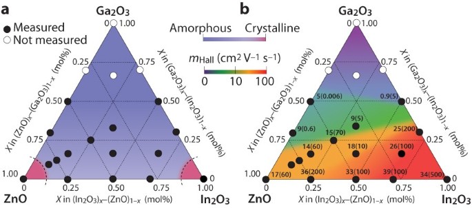
(a) Amorphous formation and (b) electron transport properties of In2O3-Ga2O3-ZnO thin films. The values in (b) denote the electron Hall mobility (cm2/V s) with density (1018 cm-3) in parentheses. Modified after Ref. 45, reproduced with permission (© 2006 JJAP).
-
4
Low operation voltage: Oxides have electronic structures specific to the ionic chemical bonds, and therefore they form much fewer defect states in the band gap than conventional covalent semiconductors such as silicon. The low defect density allows small S values of 0.1 V/decade and low operation voltages of < 5 V (Figure 2(a,b)).
-
5
Large allowance in the choice of gate insulator: In general, the choice of a gate insulator is critical for field-effect transistors including TFTs. However, a variety of gate insulators (e.g. SiO2, SiNx, SiONx, Y2O3, HfO2, Al2O330, (Ba,Sr)TiO331, organics) have been examined for AOS TFTs, and good operation characteristics have been demonstrated in each case. This feature would also benefit for two reasons: the unipolarity of AOS, by which only electrons are mobile and thus the valence band offset between the gate insulator and AOS is not critical; and the high ionic chemical bonding nature, which gives rise to fewer defects at the gate insulator/AOS interfaces.
-
6
Simple electrode structure and low off current: Silicon-based field-effect transistors require a p–n junction for the source and drain electrodes to suppress inversion operation and the consequent increase in off current. Since AOS TFTs have not exhibited inversion p-channel operation, simple metallic contacts may be used for source and drain electrodes without increasing the off current.
-
7
Excellent uniformity and surface flatness: Irrespective of the very high mobility in p-Si TFTs (> 100 cm2/V s), their applications are limited due to the difficulty in large-area mass-production and the inhomogeneity issue originating from the presence of grain boundaries. AOS TFTs exhibit excellent short-range uniformity18 and surface flatness (> 0.3 nm) owing to the amorphous structure.
-
8
Ease of fabrication: Due to the above features, such as the possibility of low-temperature fabrication, insensitivity to gate insulator, the simple electrode structure and the wide flexibility of processing temperature, it is rather easy to fabricate AOS TFTs. The conventional direct-current (DC) sputtering methods widely used for the deposition of ITO in solar cells and flat-panel displays may also be used for AOS TFTs32,33.

These features are related to the electronic structure of a-IGZO, a typical AOS, as shown in Figure 2(c). The figure shows the electronic states that control the Hall effect, n-channel TFT operation, and inversion p-channel TFT operation (details of the experimentally clarified tail states and subgap states are provided in Figures 67 8).

Carrier transport in a-IGZO. (a) Relationship between Hall mobility and carrier density for c-IGZO and a-IGZO. (b) Illustration of percolation conduction showing examples of (i) a shorter path and (ii) a longer winding path. The isosurface represents the electron potential in the conduction band.

Subgap density of states in a-IGZO obtained by the C–V method. Data for a-Si:H are shown for comparison. Ec denotes the CBM.

Effects of thermal annealing on TFT characteristics and electronic structures of a-IGZO. (a–c) Characteristics of (a) high-quality as-deposited a-IGZO TFT (HQ), (b) low-quality as-deposited a-IGZO TFT (LQ), and (c) low-quality annealed a-IGZO TFT (LQ-ann) (VDS = 4 V) (modified after Hosono et al., J. Non-Cryst. Sol. 354, 2796 (2008), reproduced with permission, © 2008 Elsevier). (d,e) Change in (d) optical absorption and (e) hard- X-ray photoemission spectra before and after thermal annealing for HQ and LQ a-IGZO films (modified after Ref. 62, reproduced with permission, © 2008 AIP).
Brief history of AOSs
Oxide TFTs have a long history that extends from the mid-1960s34,35, but there was a long lull until the report of SnO2:Sb TFTs combined with a ferroelectric gate in 199636, although some unpublished development work had been conducted. The oxide TFT fever started in 2003 with reports of several crystalline oxide TFTs using ZnO37,38,39,40 and InGaZnO441 channels. ZnO TFTs have been studied intensively because this structure is expected to exhibit better performance than a-Si:H and organic TFTs owing to the large Hall mobility (200 cm2/V s) of single-crystal ZnO and the ready formation of semiconducting crystalline thin films even on unheated substrates. However, the channels of ZnO TFTs are polycrystalline and, therefore, the TFT performance and stability suffer from the grain-boundary problems similar to the p-Si case.
A crucial problem of ZnO TFTs is the fact that ZnO is a typical transparent conducting oxide and is used as a transparent electrode in devices such as solar cells. We should remember that the most essential feature of a semiconductor is that the carrier concentration should be controllable over several orders of magnitude; oxide TFTs have been fabricated using SnO2 and ZnO, but these materials, known as good transparent conducting oxides, contain a high density of mobile electrons (typically >> 1018 cm-3) even in nominally undoped states, causing a serious problem for TFTs by making it difficult to control the channel conductance and the threshold voltage. This feature often results in instability of TFT characteristics.
Separate from the above line of oxide device development, our group started systematic material exploration of ionic oxide semiconductors in 1994 as a part of a strategy to expand the development of transparent conducting oxides42. To attain high electrical conductivity in an amorphous oxide was a big challenge because the conventional and most familiar amorphous oxide, glass, is a very good electrical insulator. We succeeded in obtaining high conductivities of up to 1 S/cm and degenerated conduction in amorphous 2CdO·GeO2 by H+/Li+ ion implantation in 199543. This result implied that while 2CdO·GeO2 was a good electrical insulator, heavy electron doping and degenerate conduction were possible by a non-equilibrium technique such as ion implantation; these features are very different from those of the crystalline transparent conducting oxides mentioned above. It was considered that this kind of amorphous oxide could be used to produce semiconducting devices with wider controllability and better stability than existing devices at the time. Along with an additional requirement that a toxic element should not be included, we chose a-IGZO, which was first reported in 200144, to develop the first AOS TFTs, and in 2004 we demonstrated the normally off operation of the a-IGZO TFT1.
Materials and processes
In this section, we discuss how to obtain stable amorphous oxide and review the AOS materials and fabrication processes. Figure 3 summarizes the structures and electron transport properties of a-IGZO films deposited at room temperature by pulsed laser deposition as a function of chemical composition45. First we should see that pure ZnO and In2O3 form crystalline films even when deposited at room temperature. This is widely observed for many metals and oxides, for which it is difficult to obtain amorphous phases. On the other hand, the binary oxide compounds, such as Zn-In-O and Zn-Ga-O, form amorphous phases if the mixing ratio of the oxides exceeds a certain threshold value. In general, mixing of two or more cations having different ionic charges and sizes is effective for enhancing the formation of an amorphous phase and suppressing crystallization; this is the reason why AOSs are basically multi-component systems, and this fact implies that we can find a rich variety of AOS materials.
Actually, many AOS materials have been reported to date since the first report of the AOS TFT. Oregon State University and Hewlett-Packard have reported the high-temperature fabrication of a-Zn-Sn-O (a-ZTO) TFTs46 and Zn-In-O (a-ZIO) TFTs47. These TFTs exhibit very high mobilities up to 55 cm2/V s although they were subjected to high-temperature annealing at 300–600 °C, giving us the expectation that AOS TFT technology will extend to high-speed circuit applications on glass and flexible substrates. For room temperature-fabricated AOS TFTs, Canon first succeeded in fabricating a-IGZO TFTs by radiofrequency (RF) magnetron sputtering48. Combinatorial approaches have been employed to screen multi-component AOS systems, including the In-Ga-Zn-O system49 and Zn-Sn-O (ZTO) system50. Other materials, such as a-In-Zn-O (a-IZO)51, a-In-Ga-O (a-IGO)14 and a-Ga-Sn-Zn-O (a-GTZO)52, have also been reported. These materials include the constituent elements of transparent conducting oxides, such as indium, zinc and tin as major constituents.
Here, let us discuss the roles of the constituent ions in the AOSs. Indium, gallium, zinc and tin are the major consistents of good transparent conducting oxides, and their unoccupied s orbitals form the electron transport paths in AOSs1,53; therefore, having a majority of these ions is the fundamental requirement to obtain AOSs with large electron mobilities. To understand the role of the other ions, it is useful to compare systems such as a-IZO and a-IGZO. As seen in Figure 3(b)45, a-IZO has higher electron mobilities than a-IGZO, but is much more difficult to control at the low electron concentrations required for TFTs (e.g. far below 1017 cm-3). As clarified by first-principles density-functional theory54, Ga–O bonds are much stronger than In–O and Zn–O bonds, meaning that the incorporation of gallium suppresses the formation of oxygen deficiencies and the consequent generation of mobile electrons. On the other hand, the incorporation of high gallium content deteriorates the electron mobility (Figure 3(b)). Therefore, the addition of an appropriate amount of a stabilizer ion that forms a strong chemical bond with the oxygen ion is important to obtain stable AOS materials and TFTs. Canon surveyed stabilizer ions (Mg, Al, Si, Ti, Ge, Mo) in the In–Zn–O system by a combinatorial approach and reported that a-In-Si-Zn-O could be an alternative candidate to a-IGZO55.
RF magnetron sputtering has been the most widely used method for depositing AOS films. It is a common production technique and is expected to be applicable for large-area mass-production. DC sputtering is an alternative candidate technique for the mass-production of AOS devices because it has benefited from the accumulation of considerable technical progress in forming large-area window electrodes for mass-produced solar cells and flat-panel displays. DC sputtering has also been reported for producing high-mobility TFTs at a substrate temperature of 100 °C32 with post-deposition annealing at 200 °C33.
Solution/wet processes for fabricating AOS TFTs have also been studied. Oregon State University and Hewlett-Packard reported the fabrication of a-ZIO TFT from a metal halide source with post-thermal annealing at 400 °C56, and the preparation of a-ZTO and a-ZIO with thermal annealing at 500 °C57 and a-IGZO with thermal annealing at 450 °C58. Recently, wet process technology has been improved significantly, and the lowest annealing temperature of 280 °C and the highest mobility of 28 cm2/V s for 600 °C-annealed a-IGZO TFT were recently reported59. Samsung Electronics reported wet-processed a-IZO TFTs60 and AM-OLED displays61.
Electronic structure of AOSs
Origin of large electron mobility
It is believed that the properties of amorphous semiconductors are considerably degraded compared with their corresponding crystalline phases, which is actually the case for silicon because intrinsic crystalline silicon (c-Si) exhibits an electron mobility of 1,500 cm2/V s, which deteriorates to less than 2 cm2/V s in a-Si:H. On the other hand, AOSs exhibit large electron mobilities of greater than 10 cm2/V s even in amorphous structures. The electronic structure shown in Figure 4 explains this behavior (see Ref. 54 for details); it benefits from the strong ionicity of oxides. In silicon, the conduction band minimum (CBM) and valence band maximum (VBM) are made of anti-bonding (sp3 σ*) and bonding (sp3 σ) states of Si sp3 hybridized orbitals, and its band gap is formed by the energy splitting of the σ*–σ levels (Figure 4(a)). By contrast, oxides have strong ionicity and charge transfer occurs from metal to oxygen atoms (Figure 4(b)), and the electronic structure is stabilized by the Madelung potential formed by these ions, raising the electronic levels in cations and lowering the levels in anions. Consequently, the CBM is primarily formed by the unoccupied s orbitals and the VBM of cations by fully occupied O 2p orbitals, as illustrated in Figure 4(c).

Schematic electronic structures of silicon and ionic oxide semiconductors. (a–c) Bandgap formation mechanisms in (a) covalent and (b,c) ionic semiconductors. (d–g) Carrier transport paths in (d) c-Si, (e) a-Si, (f) crystalline oxide and (g) amorphous oxide. (h–k) Electronic structures of defects in (h,i) silicon and (j,k) oxides. Closed and open circles denote occupied and unoccupied states, respectively. Modified after Ref. 54, reproduced with permission (© 2009 IEEE).
Owing to such an electronic structure, crystalline oxides such as ZnO, SnO2 and In2O3 have small electron effective masses of 0.25-0.35me (me is the rest mass of an electron) and reasonably high electron mobilities of 200 cm2/V s. The CBMs of these transparent conducting oxides are mainly comprised of the s orbitals of the heavy metal cations, which have large spatial sizes and spread almost spherically. The large spatial spread of the s orbitals forms a largely hybridized CBM with broad band dispersion, which is the reason for the small electron effective mass.
The above electronic structure explains why AOSs can have high electron mobilities even in amorphous structures. Conventional amorphous semiconductors such as a-Si:H exhibit much deteriorated carrier transport properties compared with the corresponding crystalline materials. This is because the chemical bonds in the covalent semiconductors are made of sp3 or p orbitals with strong spatial directivity. Therefore, the strained chemical bonds in amorphous structures form rather deep and high-density localized states below the CBM and above the VBM (Figure 4(e)), causing carrier trapping. By contrast, the CBMs of non-transition metal oxides are made of the spherically extended s orbitals of metal cations, and their overlaps with neighboring metal s orbitals are not altered appreciably by the disordered amorphous structure; therefore, the electronic levels of the CBM are insensitive to local structural randomness, and electron transport is not affected significantly (Figure 4(f,g)). This electronic structure can be verified by density functional theory, as shown in Figure 5(a). The CBM wave function can be seen to exist predominantly on the indium ions, and the calculated electron effective mass (0.2me) is close to that of c-IGZO (0.18me) and similar to that (0.35me) reported experimentally54,62.

Electronic structures of a-InGaZnO4 calculated by density functional theory. (a) Wave function (|ψ|2) of the CBM in stoichiometric a-IGZO. Green surfaces denote isosurfaces of |ψ|2 at the CBM. (b) Densities of states (total) of c-IGZO, stoichiometric a-IGZO, two oxygen-deficient a-IGZO models (VOI denotes deep occupied states type, VOII denotes shallow donor type) and hydrogen-incorporated a-IGZO (H). The energies are aligned by the O 2s level at ca. -17 eV. The lines EVBM, ECBM and EF denote the energy levels of the VBM, CBM and Fermi level. The densities of states above the EVBM are expanded by a factor of four.
Following the consideration of the electronic structure, we proposed a working hypothesis to develop good AOSs in 1996; the incorporation of heavy metal cations such as In3+ and Sn2+ is effective for forming broad-spreading CBMs even in AOSs. For TFT applications, mixing two or more cations with different ionic charges and different sizes is needed to form stable amorphous structures, and the incorporation of a stabilizer cation that has a strong chemical bond with oxygen ions is needed to better control the carrier concentration.
Percolation conduction in conduction band
As explained above, the effective mass of a-IGZO is similar to that of crystalline oxides such as crystalline IGZO (c-IGZO) and ZnO. On the other hand, the electron transport properties exhibit a peculiar behavior, as seen in Figure 6(a). First, definite Hall voltages and electron mobilities can be observed for AOSs through usual Hall measurements. This is in clear contrast to conventional covalent amorphous semiconductors such as a-Si:H for which the Hall voltages and/or Seebeck coefficients exhibit opposite signs to those expected from majority carrier polarity (the Hall voltage sign anomaly). Furthermore, the Hall mobility increases with carrier density. This trend is opposite to that observed in simple crystalline semiconductors and may be explained by percolation conduction as illustrated in Figure 6(b)54,63. In this model, a distribution of potential barriers exists in the conduction band and limits the electron mobility, and electrons take a shorter and higher conduction path at higher temperatures. This means that the mobility increases and the activation energy decreases with increasing temperature. An analysis by the percolation model64 revealed that the potential distribution is approximately 0.1 eV in height and a few tens of millielectronvolts in width (Figure 2(c))54.
Origin of low operation voltage in AOS TFTs: Few defect states
The defect states in the band gap (subgap states) are very important for semiconductor devices such as TFTs. As seen in the standard field-effect transistor theory, the source-to-drain current IDS is expressed in terms of the source-to-drain voltage VDS and gate-to-source voltage VGS as

(1) where W is channel width, L is channel length, Cg is gate capacitance, Vth is threshold voltage (a constant), and μ is the drift mobility of the majority carrier in the channel. TFT mobilities (e.g. field-effect mobility μFE and saturation regime mobility μsat) are derived from experimental IDS-VDS-VGS data based on this equation and thus correspond to the drift mobility in the ideal case. However, practically, the TFT mobilities are smaller than the drift mobility and are deteriorated by the subgap density of states (DOS), as roughly expressed by

(2) where NT is the total DOS of the unoccupied subgap DOS, and NGS = Cg(VGS - Vth) is the electron density induced by VGS. The subgap DOS also determines the operation voltage of the TFT; the operation voltage is limited by the VGS range required to switch the TFT from the off state to the on state, which is expressed by the S value defined by

(3) Here, Dsg is the subgap DOS at the Fermi level (EF). These results indicate that reduction of the subgap DOS is the most important issue for realizing high-performance TFTs.
As seen in Figure 2(b), the S value for a-IGZO TFTs may be as low as 100 mV/decade. The subgap DOS has been examined by several methods, including device simulation65 and the capacitance–voltage (C–V) method66, as shown in Figure 7. The subgap states near the CBM in a-IGZO is more than one order of magnitude lower than that in a-Si:H, and a low subgap DOS is the reason why AOS TFTs exhibit small S values and operate at low voltages. Recently, Hitachi reported the smallest S value achieved to date, 63 meV/decade, close to the theoretical limit of 59 meV/decade at room temperature, along with the lowest operation voltage of 1.5 V. This result was achieved by reducing the thickness of the a-IGZO channel to 6 nm and that of the gate insulator to 15 nm67.
The lower densities of subgap defect states can be explained by the ionic nature of chemical bonds in oxides. As illustrated in Figures 4(a) and (b), the conduction band (CB) and valence band (VB) of silicon are made of anti-bonding and bonding states of sp3 hybridized orbitals, respectively. If a silicon vacancy is created, a dangling bond state with an unpaired electron is formed near the middle of the band gap and is occupied by one electron, which acts as both an electron trap and a hole trap (Figure 4(h)), and consequently degrades the operation characteristics of both n- and p-channel TFTs. This is why the silicon dangling bonds must be passivated, such as by hydrogen, to move the subgap defects out from the band gap (Figure 4(i)). By contrast, the CB in oxides is mainly made of the unoccupied orbitals of the metal cation; therefore, the energy levels of oxygen vacancies (VO), that is, the non-bonding state of the metal cation, is formed in or near the CBM allowing the vacancies to act as a shallow donor but not as an effective electron trap (Figure 4(j)).
It should be noted that such donor states are not stable in many oxides. Even in such cases, the oxygen vacancy level is relaxed to form a fully occupied deep state as illustrated in Figure 4(k), which no longer traps an electron and is inactive for electron transport and n-channel TFTs. Density functional theory calculations confirm this view and have clarified that oxygen deficiencies form either shallow donors as in Figure 4(j) or deep occupied states as in Figure 4(k) depending on the local structure of the oxygen deficiency68 (see Figure 5(b)). The deep occupied states have been observed experimentally by hard-X-ray photoemission spectroscopy62.
Peculiar annealing effect: Insensitivity to deep occupied defects
The above electronic structure gives rise to a unique result specific to oxide semiconductors; the electron transport and operation characteristics of n-channel TFTs are rather insensitive to the history of channel fabrication and post-deposition thermal annealing for AOSs. Figures 8(a) to (c) compare the characteristics of TFTs with a-IGZO channels and different film qualities. The low-quality (LQ) films deposited under non-optimal conditions have low Hall mobility, and the high-quality (HQ) films have high Hall mobility in the as-deposited state62. The LQ a-IGZO-channel TFT shows very poor TFT characteristics, with mobility less than 1 cm2/V s, while the HQ a-IGZO-channel TFT shows a much higher mobility of 8 cm2/V s. The poor performance of the LQ a-IGZO TFT (large S value and low TFT mobility) indicates that the subgap DOS in the as-deposited channel is relatively high. The poor characteristic is improved significantly by thermal annealing at 400 °C (Figure 8(c)), and the resulting performance becomes very similar to that of the HQ a-IGZO TFT (Figure 8(a)).
We should notice that this improvement to the level of HQ-channel TFT is not directly related to the improvement in film quality in the usual sense. As observed in the optical absorption spectra in Figure 8(d), the as-deposited LQ a-IGZO has the highest subgap absorption and thus the highest subgap DOS. Thermal annealing reduces the absorption by almost half, but the remaining subgap absorption is still an order of magnitude greater than that of the as-deposited HQ a-IGZO, yet the TFT characteristics of the annealed LQ TFT are similar to those of the as-deposited HQ TFT.
Hard-X-ray photoemission spectroscopy is a powerful tool for examining the electronic state of thin films because it provides information from the bulk region at a depth of several nanometers into the film. This bulk-sensitive analysis makes it possible to extract reliable information on the bulk region even for very thin films. This method has proved that the majority of subgap absorption originates from the subgap DOS above the VBM (Figure 8(d,e)). The hard-X-ray photoemssion spectra exhibit additional, non-negligible signals in the deep subgap region above the VBM with a bandwidth of 1.5 eV. The subgap DOS is highest in the as-deposited LQ film, while that of the as-deposited HQ film is much lower. By annealing the LQ film, the subgap DOS is reduced by almost half, corresponding well to the change in the subgap optical absorption, but remains much higher than that for the HQ films.
The observation described above is explained by the high EF of AOSs. The AOS channel layers used for TFTs in general have electrical conductivities of 10-3–10-6 S/cm, which correspond to a minimum carrier density of approximately 1012 cm-3 and a deepest EF of 0.4 eV below the CBM. Because the above subgap states are > 1.5 eV deeper than EF, and therefore fully occupied by electrons, they do not act as electron traps. This means that the wide band gap (> 3.0 eV) of AOSs is key to maintaining good electron transport properties even though high-density deep defect states exist in the band gap.
These results clearly show that the formation of subgap defect states differs considerably depending on the conditions of film deposition, but thermal annealing efficiently removes the defects close to the CBM that affect electron transport. Most of the VB defects are not removed by post-deposition thermally annealing, but fortunately do not affect electron transport.
Owing to this feature, it is easy to obtain operating TFTs with AOS channels. Here we summarize a recipe for a-IGZO TFTs. For test purposes, it is a good idea to employ a silicon wafer with a 100 nm-thick thermally oxidized SiO2 surface layer for the substrate, gate electrode and gate insulator. The a-IGZO channel may be fabricated by any deposition method without substrate heating, but, to obtain an operating TFT in the as-fabricated state, the deposition conditions should be chosen so as to obtain electrical conductivities between 10-6 and 10-3 S/cm with minimal subgap optical absorption. The channel regions are better to be patterned by lithography or using a shadow mask. The source and drain electrodes may be formed on top of the a-IGZO channels from metals such as titanium oxide or indium-tin oxide. If these TFTs do not show TFT operation or satisfactory performance, thermal annealing can be performed at 300–400 °C in air or under O2 gas. In this case, it should be noted that the top metal electrodes should be formed after thermal annealing to avoid oxidation69.
Summary: Present and future issues
We reviewed the present state of AOS technology and the scientific aspects of AOS materials and TFTs from the viewpoint of their oxide-specific electronic structures. The progress in developmental research is very rapid, and improvement in our understanding of the peculiar properties of AOSs has provided much knowledge and information. However, to transfer the AOS technology to mass-production, there remain issues to be clarified and solved. It was reported that the short-range uniformity of a-IGZO TFTs is excellent and similar to that in a-Si:H TFTs owing to the amorphous structure18, but scaling up to practical substrate sizes and examining the meter-scale uniformity by a production-compatible method such as RF/DC sputtering will be required. It has also been pointed that the operation characteristics of AOS TFTs are very sensitive to the atmosphere, such as oxygen, moisture and hydrogen content54,70,71,72. These are explained by the fact that the formation of oxygen deficiencies by thermal annealing under a reducing atmosphere and the incorporation of hydrogen by thermal annealing in an H2-containing atmosphere and by ion implantation easily increases the electrical conductivity even at low temperatures around 200 °C54. As seen in Figure 5(b), the oxygen deficiencies and incorporated hydrogen act as shallow donors and generate mobile electrons68. This problem is solved by employing a top protection layer (passivation layer) composed of SiOx, SiNx or similar, which blocks the penetration and diffusion of O-, H2O- and H-related molecules71. On the other hand, this sensitivity to a reducing atmosphere and hydrogen has been utilized to form improved source and drain contacts72, and has been applied to self-alignment processes73, which are expected to lead to a simpler process for flat-panel display production.
The most serious problem is the long-term stability of TFT characteristics, but recent works have achieved threshold voltage shifts of less than 2 V and even smaller than 1 V74,75,76. Our group has reported that thermal annealing under a wet O2 atmosphere stabilizes the chemical bonds, leading to improved and stable TFT characteristics, and we have found that the true origin of the stability originates from the formation of acceptor-type electron traps formed under constant bias stress77. It has also been pointed that the instability issue in part comes from the adsorption and desorption of O- and H2O-related molecules, and the use of an appropriate passivation layer can improve the stability71.
Another issue that should be referred to is the photoresponse of a-IGZO TFTs. It has been pointed out that the threshold voltages of a-IGZO TFTs are shifted markedly by exposure to light, even at subgap energies78,79. For photonic devices, the strong photoresponse may be good news, and the photoexcited carriers in a-IGZO films appear to have long lifetimes. On the contrary, for TFTs in flat-panel displays, the photoresponse should be suppressed, or a light-masking layer should be adopted. In addition, subgap photon illumination causes a Vth shift in TFTs at negative bias80. As seen in Figures 2(c) and 8(d,e), the subgap photoresponse originates from the subgap DOS above the VBM. Thus, the subgap photoresponse will be solved by removing the deep DOS, the presence of which can be controlled to some extent by choosing appropriate deposition conditions, as seen in the comparison of HQ and LQ a-IGZO films in Figure 8.
References
K . Nomura et al., Nature 432, 488 ( 2004 ).
M . Ito, M . Kon, T . Okubo, M . Ishizaki, N . Sekine, Proc. IDW/AD05, 845 ( 2005 ).
M . Ito et al., Proc. IDW06 EP1-4L, 585 ( 2006 ).
M . Ito et al., IEICE Trans. Electron, E90-C, 2105 ( 2007 )
M . Ito et al., J. Non-Cryst. Sol. 354, 2777 ( 2008 ).
M . Ito, C . Miyazaki, N . Ikeda, Y . Kokubo, Proc. AMFPD09, S-2 ( 2009 ).
H. N. Lee et al., Proc. IDW06, 663 ( 2006 ).
M.-C. Sung et al., Proc. IMID2007, 9 – 1 ( 2007 ).
J. K. Jeong et al., Proc. IMID2007, 9 – 4 ( 2007 ).
J. Y. Kwon et al., Proc. IMID2007, 9 – 3 ( 2007 ).
J. K. Jeong et al., Soc. Inf. Display Digest 39, 1 2008 .
J. K. Jeong et al., J. Soc. Inf. Display 17, 95 ( 2009 ).
J.-H. Lee et al., Soc. Inf. Display Digest 39, 625 ( 2008 ).
J. Y. Kwon et al., Proc. AMFPD08, 287 ( 2008 ).
R. E. Presley et al., Sol. Stat. Electron. 50, 500 ( 2006 ).
M . Ofuji et al., IEEE Electron. Dev. Lett. 28, 273 ( 2007 ).
S. I. Kim et al., Int. Electron. Dev. Meeting ‘08, 1 ( 2008 ).
R . Hayashi et al., J. Soc. Inf. Display 15, 915 ( 2007 ).
P . Görrn et al., Adv. Mater. 18, 738 ( 2006 ).
H.-H. Hsieh et al., Proc. Soc. Inf. Display, P-11 ( 2008 ).
I . Song et al., IEEE Electron. Dev. Lett. 29, 549 ( 2008 ).
Y.-L. Wang et al., Electrochem. Sol. Stat. Lett. 11, H60 ( 2008 ).
J.-S. Park et al., Appl. Phys. Lett. 95, 013503 ( 2009 ).
W . Lim et al., Appl. Phys. Lett. 94, 072103 ( 2009 ).
R . Martins et al., Appl. Phys. Lett. 93, 203501 ( 2008 ).
T . Osada et al., Proc. AMFPD09, 3 – 3 ( 2009 )
T . Osada et al., Soc. Inf. Display Digest, 184 ( 2009 ).
H . Yin et al., Appl. Phys. Lett. 93, 172109 ( 2008 ).
M.-J. Lee et al., Adv. Funct. Mater. 19, 1587 ( 2009 ).
J. B. Kim, C . Fuentes-Hernandez, W. J. Potscavage, Jr, X.-H. Zhang, B . Kippelen, Appl. Phys. Lett. 94, 142107 ( 2009 ).
J. B. Kim, C . Fuentes-Hernandez, B . Kippelen, Appl. Phys. Lett. 93, 242111 ( 2008 ).
Y.-K. Moon et al., Jpn J. Appl. Phys. 48, 031301 ( 2009 ).
M.-H. Lee et al., Soc. Inf. Display Digest 40, 191 ( 2009 ).
H. A. Klasens, H . Koelmans, Sol. Stat. Electron. 7, 701 ( 1964 ).
G. F. Boesen, J. E. Jacobs, Proc. IEEE Lett., 2094 ( 1968 ).
M. W. J. Prins et al., Appl. Phys. Lett. 68, 3650 ( 1996 ).
J . Nishii et al., Jpn J. Appl. Phys. 42, L347 ( 2003 ).
S . Masuda et al., J. Appl. Phys. 93, 1624 ( 2003 ).
R. L. Hoffman, B. J. Norris, J. F. Wager, Appl. Phys. Lett. 82, 733 ( 2003 ).
P. F. Carcia, R. S. McLean, M. H. Reilly, G . Nunes, Jr, Appl. Phys. Lett. 82, 1117 ( 2003 ).
K . Nomura et al., Science 300, 1269 ( 2003 ).
H . Hosono, T . Kamiya, M . Hirano, Bull. Chem. Soc. Jpn 79, 1 ( 2006 ).
H . Hosono, N . Kikuchi, N . Ueda, H . Kawazoe, K . Shimidzu, Appl. Phys. Lett. 67, 2663 ( 1995 ).
M . Orita, H . Ohta, M . Hirano, S . Narushima, H . Hosono, Phil. Mag. B 81, 501 ( 2001 ).
K . Nomura et al., Jpn J. Appl. Phys. 45, 4303 ( 2006 ).
H. Q. Chiang, J. F. Wager, R. L. Hoffman, J . Jeong, D. A. Keszler, Appl. Phys. Lett. 86, 013503 ( 2005 ).
N. L. Dehuff et al., J. Appl. Phys. 97, 064505 ( 2005 ).
H . Yabuta et al., Appl. Phys. Lett. 89, 112123 ( 2006 ).
T . Iwasaki et al., Appl. Phys. Lett. 90, 242114 ( 2007 ).
M. G. McDowell, R.J. Sanderson, I.G. Hill, Appl. Phys. Lett. 92, 013502 ( 2008 ).
B . Yaglioglu, H. Y. Yeom, R . Beresford, D.C. Paine, Appl. Phys. Lett. 89, 062103 ( 2006 ).
E. M. C. Fortunato et al., Appl. Phys. Lett. 92, 222103 ( 2008 ).
K . Nomura et al., Phys. Rev. B 75, 035212 ( 2007 ).
T . Kamiya, K . Nomura, H . Hosono, J. Display Technol. 5, 273 ( 2009 ).
H . Kumomi et al., J. Display Technol. 5, 531 ( 2009 ).
D.-H. Lee, Y.-J. Chang, G. S. Herman, C.-H. Chang, Adv. Mater. 19, 843 ( 2007 ).
S.-J. Seo, C.G. Choi, Y. H. Hwang, B.-S. Bae, Soc. Inf. Display Digest 39, 1254 ( 2008 ).
G. H. Kim et al., Soc. Inf. Display Digest 39, 1258 ( 2008 ).
S.-Y. Han, D.-H. Lee, G.S. Herman, C.-H. Chang, AMFPD Digest, 3 – 1 ( 2009 ).
J. H. Lim et al., Appl. Phys. Lett. 95, 012108 ( 2009 ).
M. K. Ryu et al., Soc. Inf. Display Digest 40, 188 ( 2009 ).
K . Nomura et al., Appl. Phys. Lett. 92, 202117 ( 2008 ).
K . Nomura et al., Appl. Phys. Lett. 85, 1993 ( 2004 ).
T . Kamiya, K . Nomura, M . Hirano, H . Hosono, J. Display Technol. 5, 462 ( 2009 ).
H.-H. Hsieh, T . Kamiya, K . Nomura, H . Hosono, C.-C. Wu, Appl. Phys. Lett. 92, 133503 ( 2008 ).
M . Kimura, T . Nakanishi, K . Nomura, T . Kamiya, H . Hosono, Appl. Phys. Lett. 92, 133512 ( 2008 ).
T . Kawamura et al., IEEE Electron. Dev. Meeting ’08, 1 ( 2008 ).
T . Kamiya, K . Nomura, H . Hosono, Phys. Stat. Sol. A 206, 860 ( 2009 ).
K. J. Saji et al., J. Electrochem. Soc. 155, H390 ( 2008 ).
D . Kang et al., Appl. Phys. Lett. 90, 192101 ( 2007 ).
J. K. Jeong, H. W. Yang, J. H. Jeong, Y.-G. Mo, H. D. Kim, Appl. Phys. Lett. 93, 123508 ( 2008 ).
A . Sato et al., Appl. Phys. Lett. 94, 133502 ( 2009 ).
J . Park et al., Appl. Phys. Lett. 93, 053501 ( 2008 ).
Y . Park et al., Proc. IDW07, AMD9-1 ( 2007 ).
T . Riedl, P . Görrn, P . Hölzer, W . Kowalsky, Phys. Stat. Sol. (RRL) 1, 175 ( 2007 ).
Y.-K. Moon et al., Appl. Phys. Lett. 95, 013507 ( 2009 ).
K . Nomura, T . Kamiya, M . Hirano, H . Hosono, Appl. Phys. Lett. 95, 013502 ( 2009 ).
T.-C. Fung et al., J. Inf. Disp. 9, 21 ( 2008 ).
K . Takechi, M . Nakata, T . Eguchi, H . Yamaguchi, S . Kaneko, Jpn J. Appl. Phys. 48, 010203 ( 2009 ).
T.-J. Ha et al., Proc. AMFPD09, 49 ( 2009 ).
Author information
Authors and Affiliations
Corresponding author
Rights and permissions
About this article
Cite this article
Kamiya, T., Hosono, H. Material characteristics and applications of transparent amorphous oxide semiconductors. NPG Asia Mater 2, 15–22 (2010). https://doi.org/10.1038/asiamat.2010.5
Published:
Issue Date:
DOI: https://doi.org/10.1038/asiamat.2010.5
This article is cited by
-
Investigating an abnormal hump phenomenon in top gate a-InGaZnO thin-film transistors due to mobile sodium diffusion
Scientific Reports (2023)
-
Optimization of Sputtering Parameters and Their Effect on Structural and Electrical Properties of CAAC-IGZO Thin-Film Transistors
Electronic Materials Letters (2023)
-
Graphene quantum dots modulated solution-derived InGaO thin-film transistors and stress stability exploration
Rare Metals (2023)
-
Engineered disorder in CO2 photocatalysis
Nature Communications (2022)
-
Study of wide bandgap SnOx thin films grown by a reactive magnetron sputtering via a two-step method
Scientific Reports (2022)
