
Abstract
In Chap. 4, we introduced quantum mechanics as the proper alternative to classical mechanics to describe physical phenomena, especially when the dimensions of the systems considered approach the atomic scale. The concepts we learned will now be applied to describe the physical properties of electrons in a crystal. During this process, we will make use of the simple quantum mechanical systems which were mathematically treated in the previous chapter. This will lead us to the description of a very important concept in solid-state physics, namely, that of the “energy band structures.”
Access this chapter
Tax calculation will be finalised at checkout
Purchases are for personal use only
References
Chhowalla M et al (2013) Electronics and optolectronics of two –dimensional transition metal dichalcogenides. Nat Chem 5:263
Das S et al (2014) Nano Lett 14:2861
Duan X et al (2015) Review Chem Soc Rev 44:8859
Chelikowsky JR, Cohen ML (1976) Nonlocal pseudopotential calculations for the electronic structure of eleven diamond and zinc-blende semiconductors. Phys Rev B 14:556–582
Jungwirth T, Sinova J, Masek J, Kucera J, Macdonald AH (2006) Theory of ferromagnetic (III,Mn)V semiconductors. Rev Mod Phys 78:809
Further Reading
Andre G (2011) Nobel lecture: random walk to graphene. Rev Mod Phys 83
Avouris P (2010) Graphene electronic and photonic properties and devices. Nano 10:4285
Bolotin K, Sikes K, Stormer HL, Kim P (2008) PRL 101:096802
Bonaccorso F, Sun Z, Hasan T, Ferrari A (2010) Graphene photonics and optoelectronics. Nat Photonics 4:611
Bonnacorso F et al (2015) Graphene related two-dimensional crystal and hybrid systems for energy conversion and storage. Science 347(6217):1246501–1246501.
Falkovsky L (2008) Optical properties of graphene and IV-VI semiconductors. The electronic properties of graphene. Physics Uspekhi 51:887
Jungwirth T, Sinova J, Masek J, Kucera J, Macdonald AH Theory of ferromagnetic (III,Mn)V semiconductors. Rev Mod Phys 78:809 2006
Neto CAH (2009) Rev Mod Phys 81. Jan–March 2009
Peres NM, Guinea F, Castro AH (2006) Electronic properties of disordered two- dimensional carbon. PRB 73:125411
Wallace PR (1947) Phys Rev 71:622
Author information
Authors and Affiliations
Problems
Problems
-
1.
Equations of motion of an electron in the presence of an electric field.
$$ \mathrm{Assuming}\ \mathrm{a}\ \mathrm{dispersion}\ \mathrm{relation}:\varepsilon ={\varepsilon}_C+\frac{{\mathrm{\hslash}}^2}{ma^2}\left[1-\cos (ka)\right] $$-
(a)
Calculate the velocity of the electron at k = π/a.
-
(b)
If the electric field E is applied in the −x direction, derive the time dependence of k for an electron initially at k = π/a and position x = 0.
-
(c)
Derive the time dependence of the electron velocity, v(t), and the time dependence of the electron position, x(t).
-
(d)
For a = 5 nm, E = 104 V⋅cm−1, and m = 0.2 m 0, what are the maximum and minimum values of x that the electron will reach?
-
(e)
What is the period of the oscillation?
-
(f)
For the parameter of part (e), derive an expression for the effective mass as a function of k. Sketch the function.
-
(a)
-
2.
The period of the Bloch oscillations.
Consider an electron that is subjected to an electric field. The electric field exerts a force F = −qE on the electron. Assume that the electron is initially not in motion, i.e., k = 0. Upon application of the electric field, the k value of the electron increases from 0 to π/a. At this value of k, Bragg reflection occurs, and the electron assumes a k value of –π/a. Then, the electron is again accelerated to k = π/a. At this point, the electron again undergoes Bragg reflection, and the cycle starts from the beginning. The process described above is called the Bloch oscillation of the electron in an energy band of the solid-state crystal.
-
(a)
Show that the period of the Bloch oscillation is given by \( \tau =\frac{2\pi \mathrm{\hslash}}{qEa} \),
where a is the periodicity of a one-dimensional atomic chain.
-
(b)
Calculate the period of the Bloch oscillations for a = 4 Å and E = 1250 V⋅cm−1. Compare the period of the Bloch oscillations with a typical inelastic scattering times. What conclusions do you draw from the comparison? Are the Bragg reflections important scattering events for the movement of electrons in a crystal? Typical inelastic scattering times are 10−11 s for low fields and 10−13 s for high fields.
-
(a)
-
3.
Idealized electron dynamics.
A single electron is placed at k = 0 in an otherwise empty band of a bcc solid. The energy versus k relation of the band is given by:
$$ \varepsilon \left(\overrightarrow{k}\right)=-\alpha -8\gamma \cos \left(\frac{k_xa}{2}\right). $$At t = 0, a uniform electric field E is applied in the x-axis direction. Describe the motion of the electron in k-space. Use a reduced-zone picture. Discuss the motion of the electron in real space assuming that the particle starts its journey at the origin at t = 0. Using the reduced-zone picture, describe the movement of the electron in k-space. Discuss the motion of the electron in real space assuming that the particle starts its movement at the origin at t = 0.
-
4.
Effective mass.
For some materials, the band structure of the conduction band around k = 0 can be represented by \( \varepsilon \left(\overrightarrow{k}\right)=\frac{{\mathrm{\hslash}}^2}{2m}A\left({k}_x^2-\frac{a^2}{2{\pi}^2}{k}_x^4\right) \).
What is the effective mass of a free electron under these conditions?
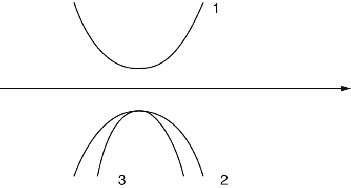
On the figure, name the different bands and point out which one of the two in the lower band has the higher effective mass.
-
5.
Calculate the coordinates of the high-symmetry point U in Fig. 5.15.
-
6.
Origin of electronic bands in materials.
Explain how electronic energy bands arise in materials.
The periodic potential in a one-dimensional lattice of spacing a can be approximated by a square wave which has the value U 0 = −2 eV at each atom and which changes to zero at a distance of 0.1a on either side of each atom. Describe how you would estimate the width of the first energy gap in the electron energy spectrum.
-
7.
Position of the Fermi level in intrinsic semiconductors.
Assume that the density of states is the same in the conduction band (N C) and in the valence band (N V). Then, the probability p that a state is filled at the conduction band edge (E C) is equal to the probability p that a state is empty in the valence band edge (E V). Where is the Fermi level located?
-
8.
Plot of the Fermi distribution function at two different temperatures.
Calculate the Fermi function at 6.5 eV if E F = 6.25 eV and T = 300 K. Repeat for T = 950 K assuming that the Fermi energy does not change. Plot the energy dependence of the electron distribution function at T = 300 K and at T = 950 K assuming E F = 6.25 eV.
-
9.
Numerical evaluation of the effective densities of states of Ge, Si, and GaAs.
Calculate the effective densities of states in the conduction and valence bands of germanium, silicon and gallium arsenide at 300 K. Note in analogy to Eq. (5.55) we have \( {N}_{\mathrm{V}}=2{\left(\frac{2\pi {k}_{\mathrm{b}}{Tm}_{\mathrm{h}}}{h^2}\right)}^{3/2} \)
-
10.
Density of states of a piece of Si.
Calculate the number of states per unit energy in a 100 by 100 by 10 nm piece of silicon (m* = 1.08 m 0) 100 meV above the conduction band edge. Write the results in units of eV−1.
-
11.
Number of conduction electrons in a Fermi sphere of known radius.
In a simple cubic quasi-free electron metal, the spherical Fermi surface just touches the first Brillouin zone. Calculate the number of conduction electrons per atom in this metal as a function of the Fermi-Dirac integral. Consider the energy at the bottom of the conduction band to be E C = 0 eV.

Rights and permissions
Copyright information
© 2019 Springer International Publishing AG, part of Springer Nature
About this chapter

Cite this chapter
Razeghi, M. (2019). Electrons and Energy Band Structures in Crystals. In: Fundamentals of Solid State Engineering. Springer, Cham. https://doi.org/10.1007/978-3-319-75708-7_5
Download citation
DOI: https://doi.org/10.1007/978-3-319-75708-7_5
Published:
Publisher Name: Springer, Cham
Print ISBN: 978-3-319-75707-0
Online ISBN: 978-3-319-75708-7
eBook Packages: EngineeringEngineering (R0)