
Abstract
An ideal crystalline solid has a periodic structure that is based on the chemical properties of its constituent atoms (see Chap. 3). However, real crystals are not perfect. They always have imperfections such as extra/missing atoms or impurities, which are called defects.
Access this chapter
Tax calculation will be finalised at checkout
Purchases are for personal use only
References
Callister WD (2000) Materials science and engineering: an introduction, 5th edn. John Wiley & Sons, Inc., New York
Wolfe CM, Holonyak N Jr, Stillman GE (1989) Physical properties of semiconductors. Prentice-Hall, Englewood Cliffs, NJ
Further Reading
Adachi S (1992) Physical properties of III-V semiconductor compounds: InP, InAs, GaAs, GaP, InGaAs, and InGaAsP. Wiley, New York, pp 263–286
Anderson JC, Leaver KD, Leevers P, Rawlings RD (2003) Materials Science for Engineers. Nelson Thornes Ltd, Cheltenham, UK
Bongiorno A, Colombo L, Diaz de la Rubia T (1998) Structural and binding properties of vacancy clusters in silicon. Europhys Lett 43:695–700
Hayes W, Stoneham AM (2004) Defects and defect processes in nonmetallic solids. Dover Publications, New York
Hurle DTJ, Rudolph P (2004) A brief history of defect formation, segregation, faceting, and twinning in melt-grown semiconductors. J Cryst Growth 264:550–564
Hurle DTJ (2004) Point defects in compound semiconductors. In: Muller G, Metois JJ, Rudolph P (eds) Crystal growth-from fundamentals to technology. Elsevier, Oxford, pp 323–343
Kittel C (1986) Introduction to solid state physics. John Wiley & Sons, New York
Murr LE (1978) Solid-state electronics. Marcel Dekker, New York
Nalawa HS, Bloembergen N, Laureate N (2000) Handbook of advanced electronic and photonic materials and devices. Academic Press, San Diego
Shaffner TJ (1997) Characterization challenges for the ULSI era. In: Rai-Choudhury P, Benton JL, Schroder DK, Shaffner TJ (eds) Proceedings of the Electrochemical Society symposium on diagnostic techniques for semiconductor materials and devices. Electrochemical Society, Pennington, NJ, pp 1–13
Swaminathan V, Macrander AT (1991) Materials aspects of GaAs and InP based structures. Prentice-Hall, Englewood Cliffs, NJ
Author information
Authors and Affiliations
Problems
Problems
-
1.
Give some examples of physical properties that defects can change.
-
2.
Identify the types of point defects shown in Fig. 19.1. Please re-sketch the figure.
-
3.
Calculate the number of vacancies per cubic meter in iron at 750 °C. The energy for vacancy formation is 1.08 eV/atom. Also, the density and atomic weight for Fe are 7.65 g⋅cm−3 and 55.85 g⋅mol−1, respectively. Assume A is unity.
-
4.
Find the equilibrium concentration of defects for T = 0, 200, 400, 600, 800, 1000, and 1200 K if the energy to form a defect is 1 eV/atom. Assume A is unity. Graph your results. For T = 1200 K, how many atoms per single vacancy are present?
-
5.
The formation energies of vacancy clusters in Si are listed below. Calculate the formation energy of (i) system a (30 single vacancies), (ii) system B (five 6-vacancy clusters), and (iii) system C (three 10-vacancy clusters). Which system has the lowest formation energy? Why?
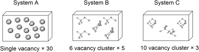
(Cluster shapes reprinted with permission from Europhys Lett Vol. 43, p. 697, Fig. 1, Bongiorno A, Colombo L, and Diaz de la Rubia T, “Structural and binding properties of vacancy clusters in silicon,” p. 697. Copyright 1998, EPD Sciences.)

Size | 1 | 6 | 10 |
Energy (eV) | 3.4 | 11.4 | 15.6 |
-
6.
Briefly describe the difference between an edge dislocation and a screw dislocation.
-
7.
Show how to find the Burgers’ vector for a screw dislocation.
-
8.
GaAs/InAs have a 7.2% lattice mismatch. How many monolayers of InAs may be grown on GaAs before a semi-coherent boundary is formed? (aGaAs = 0.565 nm aInAs = 0.606 nm, assume \( b={a}_{\mathrm{InAs}}/\sqrt{2} \)).
-
9.
What is preferential etching?
-
10.
What have been the goals of the semiconductor industry in silicon crystal growth technology? Why?
Rights and permissions
Copyright information
© 2019 Springer International Publishing AG, part of Springer Nature
About this chapter

Cite this chapter
Razeghi, M. (2019). Defects. In: Fundamentals of Solid State Engineering. Springer, Cham. https://doi.org/10.1007/978-3-319-75708-7_19
Download citation
DOI: https://doi.org/10.1007/978-3-319-75708-7_19
Published:
Publisher Name: Springer, Cham
Print ISBN: 978-3-319-75707-0
Online ISBN: 978-3-319-75708-7
eBook Packages: EngineeringEngineering (R0)