
Abstract
Developments in computing hardware are constrained by the operating principles of complementary metal oxide semiconductor (CMOS) technology, fabrication limits of nanometer scaled features, and difficulties in effective utilization of high density interconnects. This set of obstacles has promulgated a search for alternative, energy efficient approaches to computing inspired by natural systems including the mammalian brain. Atomic switch network (ASN) devices are a unique platform specifically developed to overcome these current barriers to realize adaptive neuromorphic technology. ASNs are composed of a massively interconnected network of atomic switches with a density of ∼109 units/cm2 and are structurally reminiscent of the neocortex of the brain. ASNs possess both the intrinsic capabilities of individual memristive switches, such as memory capacity and multi-state switching, and the characteristics of large-scale complex systems, such as power-law dynamics and non-linear transformations of input signals. Here we describe the successful nanoarchitectonic fabrication of next-generation ASN devices using combined top-down and bottom-up processing and experimentally demonstrate their utility as reservoir computing hardware. Leveraging their intrinsic dynamics and transformative input/output (I/O) behavior enabled waveform regression of periodic signals in the absence of embedded algorithms, further supporting the potential utility of ASN technology as a platform for unconventional approaches to computing.
Export citation and abstract BibTeX RIS
1. Introduction
The mammalian brain continues to eclipse complementary metal oxide semiconductor (CMOS) technology in performing complex tasks such as associative memory, pattern recognition and prediction, particularly in noisy and error-prone environments. Its capacity to process information arises from a complex network of functionally simple, yet evolutionarily adaptive biological neurons.1) The behavior of the brain has been proposed to emerge from a form of organized complexity, where a cooperative network facilitates efficient information storage, transfer, and processing.1) In this scenario, neurons, the individual functional units of the brain, receive, integrate, and broadcast signals with other neurons driving correlated interactions with canonical regularity.2) Extensive efforts have been made to emulate the brain's unique properties in computing hardware and software implementations, attempting to mimic the parallelism and integration of structures found in biological brains.3)
Computational frameworks inspired by the dynamics of natural systems including biological brains are generally classified as unconventional or alternative computing.4) One class of methods known as natural computing commonly involves very-large scale integration (VLSI) of complex processors or simulated neural networks on CMOS platforms for solving predefined tasks such as the Nanocell, memristor crossbar arrays, photonic reservoirs, and compliant robotics.5–8) The well-known engineering, scaling, and cost limitations of traditional CMOS technology9) necessitate disruptive innovation in both systems and hardware which are capable of rapidly processing large and diverse data sets. In order to realize transformative advances in cognitive technology, research into "more-than-Moore" strategies strive to circumvent the limitations of conventional materials and processes.
Nanoarchitectonics provides a unique framework for the rational design and scalable fabrication of functional materials from atomic and molecular building blocks. Managing the delicate balance between thermodynamic and kinetic effects through field-induced manipulation allows for the bottom-up directed-assembly of nanoscale architectures using top-down patterning. The resulting atomic switch networks extend over various scales (mm–nm) in length and complexity.10) A hardware technology developed using nanoarchitectonic concepts, the atomic switch, offers a platform to create biologically-inspired nanoscale logic and memory devices that are also CMOS compatible. The atomic switch is a memristive electroionic circuit element which provides multi-state, nonlinear switching and synapse-like memory characteristics, operating through a bias-driven filamentary switching mechanism across a metal–insulator–metal (MIM) junction.11) Despite their attractive operational characteristics, modern applications of atomic switches and other memristive systems generally involve ordered cross-bar arrays which remain subject to scaling limits similar to those for traditional CMOS.12)
The atomic switch network (ASN) is a radically divergent nanoarchitecture where individual atomic switches self-organize into a highly-interconnected network structurally reminiscent of the cortical neuropil.13) Through a top-down meets bottom up nanoarchitectonic design strategy that exploits concentration gradients and local chemical heterogeneities,10) a complex network of overlapping silver nanowire junctions grown onto a multi-electrode array is functionalized to produce Ag|Ag2S|Ag atomic switches with controllable densities of up to ∼109 junctions/cm2. The network density and topology are directed through lithographically patterned posts, acting as nucleation sites for electroless silver deposition. The ASN is far less restricted in terms of scaling limits and does not require programmable control over its component atomic switch elements. The key operational aspect of the ASN for computing applications is hierarchical causation, where top-down spatiotemporal stimulation of the network serves to produce internal dynamics resulting from the collective bottom-up interactions of its component atomic switch elements which can be monitored at the microscale and utilized. In comparison, CMOS devices exclusively utilize top-down causation whereby the program level provides deterministic instructions to the transistors whose collective properties have no bearing on the outcome.
In the network configuration, the operation of a group of atomic switches produces correlated interactions manifesting into emergent behaviors such as a constantly reconfiguring energetic potential, power law dynamics, and distributed spatiotemporal switching events.14) The distributed nonlinear dynamics of the ASN make it an ideal candidate for reservoir computing (RC), a biologically inspired computing paradigm that exhibits robust efficiency in performing computation in complex tasks.15,16) The RC framework does not require precise control over network connectivity or interactions, but instead harnesses the intrinsic non-linear dynamics of the system to transform information into higher dimensional representations. Here, next-generation ASN devices were fabricated, validated, and applied to a benchmark RC task, waveform regression, where experimental accuracies in the 70–90% range were obtained. This provides substantial evidence for the potential of ASNs as a new form of computing hardware with the capacity to circumvent typical scaling and interconnects limits required for complex cognitive computing technology in conventional computational platforms.
2. Materials and methods
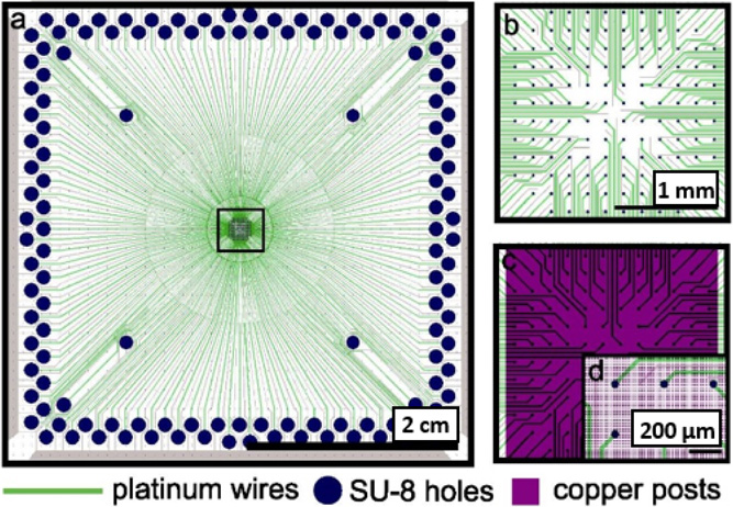
Previously reported ASN devices contained 16 measurement electrodes spaced 200 µm in a 4 × 4 grid.13,14,17,18) In order to more effectively characterize spatial dynamics within the network, next-generation devices shown schematically in Fig. 1 and measurement hardware were designed with the capacity to simultaneously record and store voltage signals from up to 128 measurement electrodes. The centrally-located network is roughly four times the area (2.5 × 2.5 mm2) of the previous generation. All measurements reported here were recorded using these next-generation devices and associated hardware. The fabrication process is shown below in Fig. 2. Point contact measurement electrodes (128) were prepared using conventional lithographic methods by patterning platinum onto a thermally oxidized (500 nm) Si wafer followed by insulation with SU-8 (300 nm). A pre-defined periodic grid of copper posts (2 × 2 × 0.5 µm3) was evaporated onto the insulating layer. This wafer was then submerged in dilute 50 mM AgNO3 (aq) to induce galvanic displacement of the copper posts with soluble Ag+ cations. The growth of silver nanowire structures through electroless deposition occurred over a period of ∼45 min. This self-organization process results in a diverse network of silver nanowires with varying wire diameters and lengths, as seen in Figs. 2(e) and 2(f). Nanoscale MIM junctions were produced by repeated exposure of the network to sulfur gas, where the junctions formed by mutual wire-to-wire contacts are converted to Ag|Ag2S|Ag interfaces. Figure 2(e) illustrates many nanowire junctions forming atomic switches in a dense network structurally reminiscent of the brain. As individual atomic switches have dimensions on the scale of nanometers, one cannot address switches individually in such a construction. However, underlying measurement electrodes do permit the application of an electrical bias into the network that can then percolate throughout the junctions.
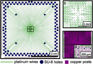
Fig. 1. Design schematics of next-generation ASN devices show 128 lithographically patterned platinum measurement electrodes (a) which are converted to point contacts with an insulating SU-8 dielectric layer, scale bar = 2 cm. Panels (b) and (c) show the central area of the device on top of which the ASN is grown, scale bar = 1 mm. Copper posts (d) patterned throughout the active area serve as nucleation sites for growth of the ASN, scale bar = 200 µm.
Download figure:
Standard image High-resolution image
Fig. 2. (a) Device substrate with a SU-8 dielectric layer creates 128 individually addressable point contact Pt electrodes (30 µm diameter, 200 µm pitch). (b) Magnified view of active device region denoted in (a) scale bar = 1 mm. (c) Active region of device substrate following evaporation of lithographically patterned Cu posts (5 µm diameter, 5 µm pitch) used as nucleation sites for the electroless growth of the ASN network, scale bar = 1 mm; (inset) magnified view of an individual input/output (I/O) electrode and Cu grid, scale bar = 50 µm. (d) Active device region following electroless deposition of Ag nanowire network, scale bar = 1 mm. (e, f) Magnified views reveal the highly interconnected nanowires of variable lengths and thicknesses, scale bars = 60 and 5 µm respectively.
Download figure:
Standard image High-resolution image3. Results and discussion
3.1. Operational validation of device performance
The criteria for functional ASN devices are: presence of distributed MIM junctions, robust memristive activity,14) and dynamical network behavior resulting from cascading interactions amongst switches throughout the network.19,20) The memory capabilities of the ASN are attributed to memristance-like behavior (memory of previous resistance states) of their component atomic switches which manifest as a time dependent nonlinear response to applied voltage. A single atomic switch is stimulated by applying a voltage bias to the junction, causing mobile silver cations to migrate to the cathode of the junction. Continued bias causes silver to aggregate at the cathode, forming a bridging filament at the MIM junction thereby increasing current flow.21) The atomic switch operates by switching between high-resistance (incomplete filament, "OFF") and low-resistance (complete filament, "ON") states. The threshold voltage between "ON" and "OFF" states is determined by the chemical composition and gap width of the individual atomic switches.21) After a filament has been completely formed, the potential difference across the junction decreases. This removes the kinetic driving force to maintain the filament, so the junction returns to the thermodynamically preferred Ag2S high resistance (OFF) state as the filament dissolves back into the insulating layer. Applying an AC voltage increases memory lifetime by diminishing electromigration effects, slowing the diffusion of formed filaments and preserving the resistance state of the switch.11)
Repeated voltage sweeps in the network verified the memristive-like non-linear characteristics observed in single junctions22) as shown in Fig. 3. The dramatic increase in conductance corresponds to filament formation where a large number of strongly memristive atomic switches reached the threshold necessary for complete filament formation. Continued sweeping of the applied bias causes a thickening of the filaments and produced fault-tolerant switching activity. Data storage on memristive devices is typically accomplished by encoding information to resistance values of individual elements. Here, embedded atomic switches are organized in hierarchal clusters to accomplish data storage utilizing inherent redundancies to produce fault-tolerant features. This characteristic enabled the use of volatile memristive elements, as opposed to non-volatile memristors found in conventional devices, to accomplish processing-in-memory for the subsequent computing experiments.23)

Fig. 3. Under a ±1.5 V sweep, the ASN device has been activated and is validated for memristive activity by the presence non-linear I V behavior.
Download figure:
Standard image High-resolution imageOne of the initial methods to verify the ASN functionality was through examination of the frequency spectrum of the current output under applied DC bias13,14) which provides evidence of network-wide switching activity. Feedback within the network's embedded atomic switches leads to complex couplings between the switches and a constantly evolving network state.14) Figure 4 presents a comparison of the power spectral density of the current output between an active network functionalized through exposure to sulfur gas (black line) and one that contains un-functionalized silver wires (grey line). The un-functionalized devices do not exhibit power-law dynamics whereas the functionalized device produces a power-law curve with a slope of β = 1.38. Previously reported devices showed a scaling factor of β = 1.34, which shows that these next-generation devices are in good agreement with the previous reports.14) The presence of power-law dynamics indicates that the ASN's dynamical activity occurs within a scale-free network. Other scale-free networks including the mammalian brain and cellular automatons have heuristically operated at the "edge of chaos" or in a "critical" regime where information transfer is maximized.24) The ASN was designed to include these features by varying copper seed size and thereby controlling the physical topology. Further, initialization of the network using voltage pulses provided enhanced and subtle control over the functional topology and correlative behavior between switches, resulting in a hierarchy of power-law dynamics.

Fig. 4. Fourier transforms of current response for an un-functionalized Ag network (grey) and functionalized Ag|Ag2S|Ag (black) network. The power spectrum of the functionalized network displays 1/fβ power law scaling (β = 1.38), indicative of spatiotemporal correlations in network activity.
Download figure:
Standard image High-resolution imageInteractions amongst atomic switches, facilitated by the recurrently connected network of silver nanowires, produce emergent, system-wide behaviors in the measured output including: 1/f noise, temporal metastability, and persistent fluctuations correlated in space and time.19,25) These network effects are in clear contrast to the case of individual atomic switches, but the embedded non-linear response of individual elements continue to operate with a memory of previous resistance states.26) When stimulated with an applied bias at one point in the network [Fig. 5(a), red dot], the atomic switches are not uniformly activated as the current flows through the network to the ground [Fig. 5(a), black dot]. Instead, the current percolates in a stochastic pathway throughout the network. The large distribution of nanowire lengths and diameters generated through the self-organized fabrication method endow each atomic switch in the network with a different set of operational parameters such as the threshold "ON" voltage. Under applied bias, the completion of a filament at one location causes a potential drop in another location, which in turn influences other connected junctions, resulting in the propagation of switching activity through internal feedback.27) These processes constantly reconfigure the network and result in time-dependent potential maps of electrical activity recorded by the measurement electrodes where cascading local or distributed switching events are readily visualized.19) Continuously evolving voltage traces are observed at points distributed throughout the network (Fig. 5) which indicate this avalanche-like effect. In this case, the unique nonlinear transformation of each voltage trace with respect to the input signal can be understood from the framework of the network's dynamic topology. Since the functional topology is not controlled and constantly changing due to the presence of switching activity, electrodes that are close in proximity may actually be more distant in their connectivity network, and vice versa. In this case, the current traveled through different pathways, and the transformations that were recorded provide a measure of the instantaneous connectivity of the switches in the network.28)
Download figure:
Standard image High-resolution image
Fig. 5. A unipolar 2 V triangle wave (inset) is input into the ASN at the red point and grounded at the black point. (a) Distributed network activity causes voltage signals that are input to the device to be transformed into higher-dimensional output representations. All 64 channels show the great diversity of behavior, and several color-coded (b) channels are plotted to show the variation in output.
Download figure:
Standard image High-resolution image3.2. Applications in natural computing/RC
The ASN is most suited to the type of unconventional computing called RC, a supervised learning framework rooted in neural network research.15) Standard simulated neural network applications, typically modelled after the brain's structure and functionality, utilize a network of nodes connected with adjustable weights to process information.29) RC was developed from the foundations of standard neural networks to overcome the computational cost of adjusting individual connective weights, and instead uses statistically distributed connective weights between nodes which do not require training or programmable control to form a "reservoir" of computation.30) RC has become an accepted method for utilizing dynamical systems (either physical or algorithmic) to perform computation due to its versatility in application, such as speech recognition, time series prediction, and pattern classification.31–33)
The ASN is one of a limited number of CMOS compatible platforms capable of performing RC.32,33) Within the context of the RC formalism, each atomic switch is a functional node in the reservoir and the connective weights between each node is mediated by the silver nanowires. The multi-electrode array on which the network is grown can be adjusted to control input and readout functionality of the electrodes to measure all the nodes in 10–50 µm regions of the network. All necessary criteria such as short-term memory, increased fault tolerance, and an arbitrarily scalable number of higher-dimensional outputs are fulfilled by the ASN.34) The memristive behavior of individual atomic switches bestows the ASN with a fading memory characteristic. This ensures that previous inputs to the network do not exert considerable influence over the current state.23) The power-law dynamics (Fig. 4) indicate that the system has a scale-free topology that allows it to operate in an "edge-of-chaos" dynamical regime providing a balance between memory and instability. The non-linear transformations Fig. 5 are an intrinsic behavior of the system that can be harnessed to increase performance. These transformations manifested as separable unique voltage signals and are a consequence of the input signal entering a higher representational space, that is then used in reconstructing the desired target waveform.23) One might think of this method as "casting a net" to catch many possible solutions where the bigger the net the more that can be caught.
Previous simulations of ASNs have indicated that the system has the fundamental capacity to perform waveform regression.20) From simulation results, performance depended on the level of higher harmonics produced and the harmonic distortion required for the specific task. For example, the cosine task only requires a shift in its periodicity and, therefore, does not require extensive higher harmonic generation. Conversely, the square wave task requires infinitely distributed harmonics to produce a straight line through wave interference. Further, voltage dependent simulations showed that increasing device activation controlled harmonic generation. Here, the device was expected to perform in a similar way with task difficulty increasing from cosine, triangle, sawtooth, and square due to increasing harmonic requirements.
Experimental performance of various waveform regression tasks using ASN devices are presented in Fig. 6. To implement waveform regression the ASN was stimulated with a bipolar sinusoidal voltage, inducing switching activity and placing the network in an active state. The output potentials measured at each electrode were then combined using the Moore–Penrose linear regression and optimized during a training period.20,35,36) Two-second epochs of data were used to evaluate the ASN's computational capability, where one second of data was allocated each for training and testing. Performance was measured during a one-second period after training where the ASN accomplished various tasks (Fig. 6). The performance of the ASN was quantified by calculating the normalized mean squared error between the target and generated waveforms.36) Here, the difference between error and unity was used to calculate accuracy.

Fig. 6. Computation of a sinusoidal wave into various waveforms. The above figure shows several waveforms (sawtooth, square, triangle, and cosine) produced using the ASN as a computational device using the setup in Fig. 4. Each plot contains the desired signal (red) and the computed signal (blue) with their accuracy w.r.t. the desired signal shown above the curves. All tasks share an 11 Hz frequency for their input waveforms and share the same dataset with only differences in the target task. The dataset was approximately 1 min long, divided into 2 s epochs, and 1 s within each epoch was allocated for training and testing. A 1 s excerpt which best represents device behavior during testing are shown above.
Download figure:
Standard image High-resolution image
The ASN was capable of achieving up to ∼90% accuracy using 62 of the 64 measurement electrodes for each task. Task complexity increased from cosine to square wave due to increasing mismatch between the sinusoidal input and the target waveform. In the case of cosine generation, the overall waveform of the input is preserved save for a shift in its periodicity. The cosine generation was the simplest task where the ASN performed with the highest accuracy, ∼90%. Note that the cosine regression shown in Fig. 6(a) would not be possible using a grid of regular resistors due to their intrinsic linear response. Because individual atomic switches have a non-linear memristive response, it is possible to harness that state function into the highly recurrent structure of the ASN. The highly recurrent structure allowed higher levels of coupled interactions that cannot be captured by a single atomic switch resulting in emergent behaviors. Particularly, the network was capable of producing delayed responses and enabled the network to shift the phase of the input signal by a half-wavelength, producing a cosine.
Figure 6(b) shows hardly any mismatch in the triangle generation, achieving a similar ∼90% accuracy and visually validates the performance metric used throughout our analysis. A similar argument is used to explain the high performance of the triangle wave when compared to the cosine task. The determining factor for reservoir performance is the level of similarity between the target and input signal, where the reservoir acts as a transformational operator to minimize dissimilarities. In both cases, the target waveform is aesthetically similar to a sinusoidal wave and maintains the overall shape of the input signal. Despite steeper edges in the triangle task, the algorithm is able to correct any differences by selectively combining different representations produced by the ASN.
The ASN generated sawtooth [Fig. 6(c)] waveforms with similar accuracy to previously reported simulations of memristive networks at roughly 90% accuracy.37) Despite the requirement to produce an instantaneous drop, the ASN delivered the sawtooth waveform with astounding accuracy. Figure 6(c) illustrates significant mismatch between the target and generated waveforms at the turning point leading to a minor drop in accuracy. Basic visual inspection shows the sawtooth task retains the overall shape of the sinusoidal input while the square wave task requires complete transformation of the input signal into a two-valued function.
Figure 6(d), on the other hand, shows significant mismatch throughout the series. The square wave generation was carried out with roughly 78% accuracy, which was much lower than the accuracy of the other tasks. To recreate a straight horizontal line, an infinite series of higher harmonics is necessary in order to satisfy the spectral theorem in the algorithm.20) Fourier analysis showed that the square wave task was relatively selective in utilizing the higher harmonics to construct the waveform. While the sawtooth and square wave both require an infinite series of sinusoidal harmonics, the square wave requires continuous constructive interference patterns to produce a horizontal line, which limits it to odd or even harmonics and drastically diminishes the regression algorithm. In this case, the ASN was only capable of producing a finite number of higher harmonics. However, further post-processing such as setting a threshold on the voltage to binarize the data can be performed to expand the device's response to a square wave input, a necessity for reliable Boolean logic computing.38)
It was found that the ASN was capable of replicating computing performances typical of reservoirs with 103 output signals.39) Theoretical studies predicts the performance to scale with an increasing number of output signals due to the dependence on the regression algorithm.23) However, how can a reservoir with much fewer output signals outperform reservoirs with output signals orders of magnitude higher than the ASN? Further inspection of the mathematical formalism23) show that performance is additionally characterized by the uniqueness of each output signal. Obtaining a set of unique signals allows us to linearly combine the output signals into a number of unique solutions, where the number of unique solutions scales with the number of unique output signals. The larger set of solutions increases the size of the "net" we cast which increases the probability and approximation of producing the correct solution.
4. Conclusion
Nanoarchitectonic concepts have been utilized to design and fabricate next-generation ASN devices including 64 measurement electrodes. Nanoarchitectonics allows for the atomic switch connection density as well as nanowire dimension distribution to be tailored using bottom up approaches combined with top down control of the copper seed pattern and post-sulfurization to create a dynamic network. Observations of memristive switching, power-law dynamics, and spatio-temporal fluctuations validate their functionality and confirm the ASN to be a dynamic, non-linear system guided by interacting atomic switches with a fading memory capacity. The device output was shown to exhibit spatially distinct, nonlinear transformations, serving to increase the dimensionality of any input signal. ASN devices have been applied to the benchmark task of waveform generation using reservoir computing, a growing field which harnesses analog computation already present in dynamical systems. The high degree of accuracy with which ASNs were able to regress varying well-known waveforms supports the conclusion that their inherent dynamics make it perfectly suited for potential high-level computing applications.
Acknowledgements
The authors would like to thank Audrius Avizienis, Cristina Martin-Olmos and Henry Sillin for their past contributions to this work as well as Juan Pablo Carbajal for many useful discussions. This work was partially supported by the Ministry of Education, Culture, Sports, Science and Technology (MEXT) World Premier International (WPI) Research Center for Materials Nanoarchitectonics (MANA) and the Semiconductor Research Corporation (2014-EP-2578). The authors acknowledge use of the Integrated Systems Nanofabrication Cleanroom (ISNC) at the University of California, Los Angeles.