
Abstract
Scanning nonlinear dielectric microscopy (SNDM) can easily distinguish the dopant type (PN) and has a wide dynamic range of sensitivity from low to high concentrations of dopants, because it has a high sensitivity to capacitance variation on the order of 10−22 F/ . It is also applicable to the analysis of compound semiconductors with much lower signal levels than Si. We can avoid misjudgments from the two-valued function (contrast reversal) problem of dC/dV signals. Under an ultrahigh-vacuum condition, SNDM has atomic resolution. As the extended versions of SNDM, super-higher-order SNDM, local-deep-level transient spectroscopy, noncontact SNDM, and scanning nonlinear dielectric potentiometory have been developed and introduced. The favorable features of SNDM originate from its significantly high sensitivity.
Export citation and abstract BibTeX RIS
1. Introduction
Scanning nonlinear dielectric microscopy (SNDM), which is used to observe dielectric polarization distribution on the surfaces of solid-state materials and carriers and fixed electric charge distribution in semiconductor devices and materials with high sensitivity and high resolution, was originally invented and developed in Japan.1) This capacitance microscopy has an extremely high sensitivity of 10−22 F/ . Therefore, it can detect even very weak nonlinear dielectric phenomena in dielectric materials. Using SNDM, we have measured and observed the ferroelectric polarization distribution,2) fixed charge distribution in a semiconductor flash memory,3–5) carrier distribution in semiconductor devices, and depletion layers in PN junctions. Moreover, next-generation ultrahigh-density ferroelectric data storage based on SNDM has also been developed.6,7)
Next, we developed higher-order scanning nonlinear dielectric microscopy (HO-SNDM), which has a higher lateral resolution realized by measuring higher-order nonlinear dielectric constants.8) On the basis of this HO-SNDM, we developed a new noncontact scanning nonlinear dielectric microscopy (NC-SNDM) that shows no resolution degradation caused by tip abrasion, and we have succeeded in achieving the world's first atomic resolution (observation of atomic dipole moment) in dielectric measurements using NC-SNDM.9–16)
Recently, we have succeeded in developing super-higher-order scanning nonlinear dielectric microscopy (SHO-SNDM), which can detect nonlinear terms up to the sixth order (sixth-order harmonic component).17,18) On the basis of SHO-SNDM, a new local-deep-level transient spectroscopy (local-DLTS) for visualizing the two-dimensional distribution of interface traps has also been developed. Moreover, a new NC-SNDM-based quantitative surface potentiometry method named scanning nonlinear dielectric potentiometry (SNDP) has been proposed.19,20) It is a unique method of detecting the local surface potential generated only by the surface dipole moment.
SNDM can be applied to the measurement and evaluation of semiconductor devices, and the dopant type (PN) can be easily distinguished and dopant distribution can be imaged over a wide dynamic range from very low to very high carrier concentrations. Moreover, SNDM is also applicable to the analysis of compound semiconductors with much lower signal levels than that from Si. We can avoid misjudgments caused by the two-valued function (contrast reversal)21) problem of dC/dV signals, because we can measure a dc capacitance component without performing voltage differentiation by SNDM. As higher-order differential coefficients (or higher harmonic components) can be detected, the local capacitance vs voltage (C–V) curve can be obtained at each pixel.
The above-mentioned advantages of SNDM over other capacitance microscopies [i.e., scanning capacitance microscopy (SCM), scanning microwave microscopy (SMM), and scanning microwave impedance microscopy (sMIM); their reported sensitivities in the dC/dV mode range from 1.1 × 10⁻¹⁷ F/ (actual)22) to 3 × 10⁻²¹ F/
 (optimal)23) and 2.1 × 10⁻²¹ F/
 (operating)24)] come from its exceptionally high sensitivity characteristics to capacitance variation of SNDM. In this review paper, among the above-mentioned SNDM measurements, we focused on the semiconductor evaluation technology and carried out measurements by SNDM.
2. Principle of SNDM
Figure 1 shows a schematic diagram of the (contact type) SNDM setup. The tip–sample contact force is kept constant by a commercial SPM controller using the optical lever method of contact atomic force microscopy (AFM). The capacitance sensor, which is called the SNDM probe in this paper, is composed of a GHz-range free-running active inductance and capacitance (LC) oscillator with a conductive cantilever tip attached. When the tip touches the surface of a specimen, the oscillating frequency f0 of the SNDM probe is determined by the static capacitance C0 (including built-in and stray capacitances) and the tip–sample capacitance Cs(t). The oscillating frequency deviation Δf(t) is proportional to the tip–sample capacitance variation ΔCs(t), which is modulated as a function of the applied ac voltage Vs(t) = Vs,0 cos ωst between the tip and the sample. Note that we apply ac bias voltage from the sample to the tip, so that the sign of voltage is defined by the sign of the sample voltage throughout this paper.
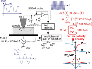
Fig. 1. Schematic diagram of SNDM.25)
Download figure:
Standard image High-resolution imageThe relationship between Δf(t) and ΔCs(t) is given by

where ΔCs(t) is proportional to a demodulated FM signal of the SNDM probe, for which we used an FM demodulator and a lock-in amplifier.26)
Figure 2 shows a typical contact-type SNDM probe and its internal structure with a circuit diagram. The noncontact-type SNDM will be mentioned later in Sect. 10. The basics of detecting a capacitance change with high sensitivity are as follows: (1) reduce the stray capacitance (or stray impedance) existing from the tip to the capacitance sensor to be as low as possible, and (2) make the ratio of the frequency deviation Δf to the center frequency (carrier frequency) f0 (i.e., Δf/f0) as large as possible when the frequency deviation Δf is demodulated. The SNDM probe contains an LC self-oscillator, and the conductive cantilever tip is attached directly to the LC resonator, which determines the oscillating frequency f0 so that the increment in stray impedance including stray capacitance is prevented. One transistor in the circuit is for oscillation and the other one is for amplification of the oscillated signal. As shown in Fig. 2, the 4 GHz probe is very small, about 4 × 4 mm2, so that capacitance variation can be immediately detected below the tip with high sensitivity by oscillating the probe just on the observation position. Moreover, as SNDM employs the frequency modulation/demodulation technique, the center frequency f0 can be arbitrarily down-converted without sacrificing Δf by using the heterodyne technique, which contains the information of capacitance variation, so that Δf/f0 can be increased freely.
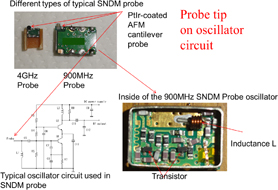
Fig. 2. Contact-type SNDM probe.25)
Download figure:
Standard image High-resolution image3. High sensitivity of SNDM
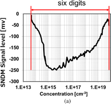
Figure 3 shows SNDM signal variation as a function of carrier concentration in silicon (Si) samples.27) It is shown that SNDM has a six-digit dynamic range and can detect even a very low concentration of 5 × 1013 cm−3 with a sufficient signal-to-noise (S/N) ratio. This data was taken using a very sharp PrIr-coated cantilever tip with a tip radius of 25 nm. This means that, using SNDM, we can perform high-resolution measurements without using a thick tip to gain a sufficient S/N ratio. Taking advantage of its high-resolution characteristic, we performed the quantitative measurement of carrier distribution in a fine cross-sectioned semiconductor device (Si-MOSFET). For example, one result is shown in Fig. 4.28) Both the polarities and concentration distribution of carriers in a very fine transistor with a channel length of about 40 nm are clearly visualized. In this quantitative measurement, both standard p- and n-type Si staircase samples were prepared for the calibration of carrier density. The carrier density of each layer has been determined by secondary ion mass spectroscopy (SIMS) measurements. The standard Si samples were polished at the same time as the cross-sectioned Si-MOSFET sample. Therefore, it was assumed that the Si-MOSFET and standard samples have the same surface conditions. The standard samples were measured after SNDM measurement of the Si-MOSFET sample. Using the data from the standard samples, we can calibrate the carrier concentration of the Si-MOSFET sample.
Download figure:
Standard image High-resolution image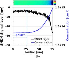
Fig. 3. SNDM signal variation as a function of carrier concentration in Si.33)
Download figure:
Standard image High-resolution image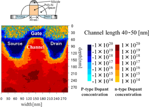
Fig. 4. Quantitative measurement of carrier distribution in a fine cross-sectional semiconductor device (Si-MOSFET).25)
Download figure:
Standard image High-resolution imageOn the other hand, measurement of the low-concentration doping region in the recently developed power semiconductor device is very important, i.e., in the power semiconductor device, low-concentration doping has been widely used to ensure high breakdown voltage. Moreover, compound semiconductor materials for high-power device applications, such as silicon carbide (SiC), produce much weaker dC/dV signals than Si. Therefore, SNDM, which can measure low-concentration regions of power devices made of such materials with high S/N ratios, is ideal for the evaluation of next-generation power semiconductor devices.
4. Avoidance of contrast reversal problem
In SCM measurement, the misjudgment of carrier concentration is a serious problem. It is caused by the two-valued function problem, that is, contrast reversal,21) when the carrier concentration in a semiconductor device is measured using the dC/dV method. This phenomenon can be explained using simplified C–V curves as a function of carrier concentration, as shown in Fig. 5. The depletion layer capacitance formed under the tip decreases from Cmax as a function of applied voltage owing to the MOS interface variation from the region of majority carrier accumulation to the depletion region. The magnitude of dC/dV at the origin increases with decreasing carrier concentration, to a certain extent, owing to depletion layer expansion under the tip. However, when the carrier concentration decreases to that in the intrinsic semiconductor region, the MOS capacitance between the tip and the semiconductor becomes constant, as determined from the dielectric constants of the semiconductor wafer and oxide layer. This is because semiconductors can be regarded as dielectrics in this intrinsic region, so that capacitance variation no longer occurs and the capacitance between the tip and the semiconductor has a constant Cmin resulting in dC/dV of zero. Therefore, at a certain carrier concentration, dC/dV, i.e., the gradient of the C–V curve at the origin, gradually declines. As a result, dC/dV becomes a two-valued function of the applied voltage V with a peak value at a certain carrier concentration. This is a very simplified explanation of the contrast reversal phenomenon. As a matter of course, misjudgment in the quantification of carrier concentration more likely occurs owing to contrast reversal when we use the dC/dV method.
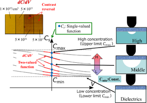
Fig. 5. Schematic C–V curves as a function of carrier concentration and dC/dV signal variation in standard staircase Si sample.25)
Download figure:
Standard image High-resolution imageHowever, it is clear, from the same figure, that the static capacitance Cs between the tip and the sample is a single-valued function of carrier concentration. Although Cs does not have information of carrier polarity as opposed to dC/dV, we can avoid misjudgment caused by the contrast reversal problem by measuring Cs directly. SNDM can also measure dc capacitance as well as its differentiation dC/dV.2) However, a much easier way without the contrast reversal phenomenon is to measure dC/dz instead of the direct measurement of dc capacitance. A schematic diagram of the dC/dz method (In Sect. 6, we call this method dC/dz-SNDM) is shown in Fig. 6. It is a very simple method because we only have to let the cantilever tip vibrate immediately above the sample surface and synchronized detection can be carried out to gain a sufficient S/N ratio. However, dC/dz signals must be obtained at a position very close to the sample surface, so that the amplitude of cantilever tip vibration is restricted to about 5 nm. Thus, the high sensitivity of SNDM to capacitance variation is indispensable.
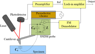
Fig. 6. Schematic diagram of dC/dz method (dC/dz-SNDM).25)
Download figure:
Standard image High-resolution imageAs shown in Fig. 7, the magnitude of the tip–sample distance dependence is a single-valued function of dc capacitance, so that dC/dz also becomes a single-valued function of carrier concentration without contrast reversal. However, as the polarity of carriers can be determined only by the dC/dV method (the dC/dz method cannot distinguish carrier polarity), it is necessary to perform both dC/dz and dC/dV measurements simultaneously. By combining the results of dC/dz and dC/dV measurements, we can obtain the correct carrier concentration. SNDM can easily perform those two measurements simultaneously.
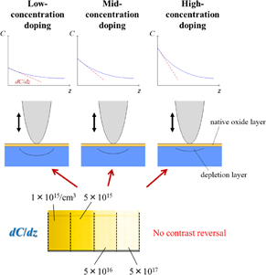
Fig. 7. Avoidance of contrast reversal problem using dC/dz method.25)
Download figure:
Standard image High-resolution image5. Measurement of compound semiconductor devices
Unlike Si, wide-band-gap compound semiconductors for next-generation power device applications, such as SiC, produce smaller dC/dV signals; thus, it is difficult to detect the signals, especially in the drift region with low carrier concentrations, by conventional methods such as SCM. Moreover, it is also difficult to measure the low-carrier-concentration region of wide-band-gap compound semiconductors even by resistance measurement methods such as scanning spread resistance microscopy (SSRM). In addition, SiC is a very hard material; therefore, SSRM cannot be applied to SiC owing to the insufficient mechanical strength of the tip.
In contrast, SNDM can be applied to all kinds of compound semiconductor since it has a high sensitivity. As an example, the result of SNDM measurement of the carrier distribution in a SiC-MOSFET is shown in Fig. 8. Even in the n− area with a very low carrier concentration, the carrier distribution is clearly imaged with a sufficient S/N ratio, which once again confirms the high sensitivity of SNDM.18)
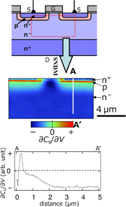
Fig. 8. SNDM measurement result of carrier distribution in SiC-MOSFET. Reprinted with permission from Ref. 18. © 2014 American Institute of Physics.
Download figure:
Standard image High-resolution imageMoreover, as SNDM can measure dielectric polarization as well as carrier distribution, both the polarization distribution and the two-dimensional electron gas in an AlGaN/GaN heterostructure were simultaneously detected.29) An example of a measured result is shown in Fig. 9.
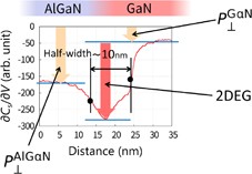
Fig. 9. Profiles of SNDM signal of AlGaN-GaN heterostructure.25)
Download figure:
Standard image High-resolution image6. Measurement of monocrystalline Si solar cells
The performance of Si solar cells is dependent on the active dopant distribution in the emitter. The estimation of the dopant distribution in a Si solar cell is difficult owing to the pyramidal surface texture of the emitter. Here, we investigate the active dopant (carrier) distribution in a phosphorus (P)-implanted Si solar cell by SNDM.30) SNDM (dC/dV) and dC/dz-SNDM are complementarily applied to visualize the carrier distribution in a cross section of the Si solar cell. The carrier density in the emitter is calibrated using SNDM data taken from standard Si samples.21) Figures 10(a)–10(c) show the obtained images of a cross section of the P-implanted emitter: (a) topography, (b) SNDM (dC/dV), and (c) dC/dz-SNDM images. The dashed line indicates the SiN/Si interface. The red and blue regions in Fig. 10(b) are the n-type and p-type regions, respectively. The bright region in Fig. 9(c) is the high-carrier-concentration region.
Download figure:
Standard image High-resolution image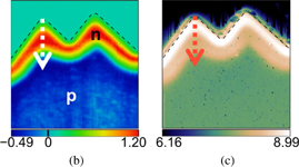
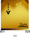
Fig. 10. (a) Topography, (b) SNDM (dC/dV), and (c) dC/dz-SNDM images of texture structure of Si solar cell. Reprinted with permission from Ref. 30. © 2017 American Institute of Physics.
Download figure:
Standard image High-resolution imageThe line profiles in Figs. 10(a)–10(c) are shown in Fig. 11. The SNDM signal level in the emitter has a peak at an intermediate position because of the contrast reversal phenomenon. In contrast, the dC/dz-SNDM signal level tends to monotonically decrease from the texture surface to the bulk, which means that the electron density decreases from the texture surface to the bulk monotonically. Thus, we can avoid misjudgment caused by the two-valued function problem named the contrast reversal phenomenon.
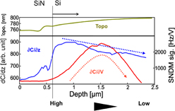
Fig. 11. Line profiles of topography, SNDM (dC/dV), and dC/dz-SNDM in Fig. 10.
Download figure:
Standard image High-resolution imageThe standard samples were measured by SNDM after SNDM measurements of the solar cell. Figure 12(a) shows the calibration curves, which show the relationship between SNDM (dC/dV) signal level and carrier density. We assumed that the dopants in the standard samples were perfectly activated. The calibration curve was calculated by the least-squares method.
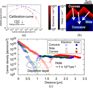
Fig. 12. (a) Calibration curves showing the relationship between SNDM signal strength and carrier density. (b) Carrier density image converted using these calibration curves. (c) Line profiles of carrier distribution. Reprinted with permission from Ref. 30. © 2017 American Institute of Physics.
Download figure:
Standard image High-resolution imageThe SNDM image in Fig. 10(b) was converted to a carrier density image using this calibration curve, and the result is shown in Fig. 12(b). The line profiles in Fig. 12(b) are shown in Fig. 12(c). The electron density decreases exponentially from the texture surface to the bulk. This is the first demonstration of quantitative carrier distribution measurement in the three-dimensional texture structure of a Si monocrystalline solar cell.
7. Development of SHO-SNDM
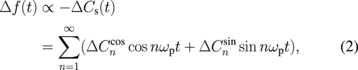
Recently, a new SNDM method, which measures not only the dC/dV term but also higher-order differentiation terms, has been developed. By this method, we can obtain much more precise physical information of materials and devices. We name this technique SHO-SNDM.18) We can easily reconstruct the C–V curve at each pixel by this method. As a result, the analysis capability is drastically improved. Basically, SHO-SNDM uses the same setup as that of conventional SNDM except for the use of a multichannel lock-in amplifier. When SHO-SNDM measurement is performed, we detect higher-harmonic components, as illustrated in Fig. 1, differently from conventional SNDM measurement, which detects the first-order harmonic component dC/dV only. The oscillating frequency deviation Δf(t) is proportional to the tip–sample capacitance variation ΔCs(t), which is modulated as a function of the applied ac voltage V(t) = Vp cos ωst between the tip and the sample. The relationship between Δf(t) and ΔCs(t) is given by
where  and
and  are the Fourier coefficients. Thus,
  and
and  are obtained by extracting the n-th-order harmonic component in ΔCs(t), which is proportional to a demodulated FM signal of the SNDM probe.
  directly correlates with the delay in the capacitance response to the applied voltage, so
  indicates no delay. The C–V curve is reconstructed from a combination of ΔCs(t), which is calculated from
  and
and  , and V(t) using time t as a parameter. The obtained C–V curve is not affected by slow minority-carrier generation because a relatively high frequency ac bias voltage is applied. The measurement of the higher-order differentiation term is equivalent to the detection of each harmonic of Fourier series expansion, so that SHO-SNDM is very useful for solving several problems in semiconductor evaluation and characterization.
8. Visualization of depletion layer and gate-bias-induced carrier redistribution in SiC-MOSFET by SHO-SNDM
Depletion layer distribution analysis based on the shape of the reconstructed C–V curve is possible. The C–V curve is obtained by plotting ![$[C_{\text{s}}(t),V(t)]$](https://content.cld.iop.org/journals/1347-4065/56/10/100101/revision1/IR170002if030.gif) on the V–Cs plane at various t in the range of −π/ωp and +π/ωp. C–V curves with monotonic increase and decrease are obtained when the tip is on the p- and n-type areas, respectively. When the tip is on the depletion layer, a V-shaped C–V curve is expected since the capacitance under the tip is affected by the type of carrier (p- or n-type). We consider the situation where the tip is on the depletion region. When the bias V becomes negative, electrons from the n-type region approach the tip, which increases Cs. When V becomes positive, Cs also increases since holes from the p-type region approach the tip. Therefore, in the depletion region, a V-shaped C–V curve is obtained.18,31) This effect reflects a contribution to the tip–sample capacitance from both the p- and n-type regions.
on the V–Cs plane at various t in the range of −π/ωp and +π/ωp. C–V curves with monotonic increase and decrease are obtained when the tip is on the p- and n-type areas, respectively. When the tip is on the depletion layer, a V-shaped C–V curve is expected since the capacitance under the tip is affected by the type of carrier (p- or n-type). We consider the situation where the tip is on the depletion region. When the bias V becomes negative, electrons from the n-type region approach the tip, which increases Cs. When V becomes positive, Cs also increases since holes from the p-type region approach the tip. Therefore, in the depletion region, a V-shaped C–V curve is obtained.18,31) This effect reflects a contribution to the tip–sample capacitance from both the p- and n-type regions.
To verify the above analysis, we measured a cross-sectional SiC-MOSFET by SHO-SNDM. Figure 13 shows two-dimensional distributions up to the sixth harmonic component. Figure 14 shows typical C–V curves (reconstructed at each pixel) and the result of visualization of the depletion layer. As mentioned above, from the shape of the C–V curve at each pixel, we can judge the type of the pixel, i.e., p-type, n-type, or depletion layer (p-type, monotonic increase; n-type, monotonic decrease; depletion layer, V-shaped). Then, the distribution of the depletion layer was clearly visualized.
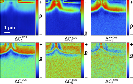
Fig. 13. Acquired images of  (n = 1, 2,..., 6). Reprinted with permission from Ref. 18. © 2014 American Institute of Physics.
Download figure:
Standard image High-resolution image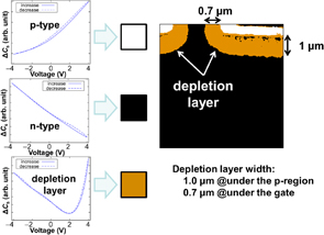
Fig. 14. Typical C–V curves and the result of visualization of depletion layer. Reprinted with permission from Ref. 18. © 2014 American Institute of Physics.
Download figure:
Standard image High-resolution imageNext, by extending SHO-SNDM, the operand measurement of the gate–source voltage VGS dependence of carrier redistribution was performed.32) In this study, an arbitrary VGS was applied between the gate and the source of the SiC-MOSFET. The results are shown in Fig. 15. It is clearly visualized that when the gate is negatively biased, the channel under the gate closes. On the other hand, when the gate is positively biased, an electron channel is formed and the n− drift area and n+ source areas are electrically connected.
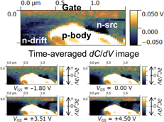
Fig. 15. Reconstructed ∂Cs/∂VS images for various gate–source voltages.25)
Download figure:
Standard image High-resolution imageAs described above, it was clearly shown that SHO-SNDM is very effective for the visualization of the depletion layer in semiconductor devices and carrier distribution in operated devices.
9. Local-deep-level transient spectroscopy for investigation of MOS interface traps based on SHO-SNDM
The physical properties of the metal–oxide–semiconductor (MOS) interface are critical for semiconductor devices. There are several techniques of characterizing MOS interface properties. Deep-level transient spectroscopy (DLTS)33) is one of the powerful techniques capable of the macroscopic quantitative evaluation of trap density at/near the MOS interface (Dit). However, it can be easily imagined that actual traps are not homogeneously distributed but have two-dimensional distributions in the atomic scale and even in the mesoscopic scale. Therefore, it is very important to characterize the MOS interface microscopically. Unfortunately, it is impossible to observe such inhomogeneity by conventional macroscopic DLTS methods. Moreover, to the best of our knowledge, scanning-capacitance-microscopy-based two-dimensional DLTS imaging has never been reported.
Here, a new technique for local DLTS imaging based on SHO-SNDM is proposed. This method enables us to observe the two-dimensional distribution of trap density at/near the MOS interface; this is demonstrated with oxidized SiC wafers.
In local-DLTS measurement, the conductive sharp tip comes in contact with the surface of an SiO2/SiC sample, which forms a tiny MOS capacitor whose capacitance Cs is modulated by external pulse voltage application. The voltage waveform applied to a sample is shown in Fig. 16(a); the dc bias and filling pulse bias with a duration of tpw are Va and Vb, respectively. The voltage-induced capacitance variation ΔCs(t) is measured through the modulation of the oscillating frequency of a free-running GHz-range LC oscillator (SNDM probe). When the voltage pulse is repeated at a frequency of fp, ΔCs(t) can be expressed as a Fourier expansion similarly to Eq. (2). As illustrated in Fig. 16(b), the waveform of Cs(t) consists of an abrupt capacitance increase (ΔCM) at t = −tpw, which is caused by the electron capture at interface traps and the gradual capacitance recovery to the original capacitance Cs0 denoted as Ctr(t) owing to the release of trapped electrons. Assuming that Ctr(t) can be expressed by decay functions with time constants τk (k = 1, 2,..., Nt), Ctr(t) is expressed as
where τk and C(τk) are the time constant and magnitude of the corresponding exponential transient. The analysis of an and bn can yield C(τk) and ΔCM, respectively. In this paper, C(τ)/ΔCM is defined as the local-DLTS signal and its plot as a function of τ is defined as the local-DLTS spectrum.
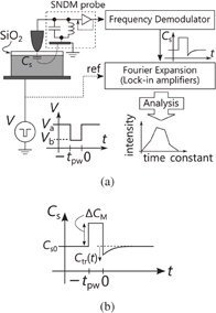
Fig. 16. Principle of local-DLTS. (a) Block diagram of the measurement system, where free-running LC oscillator with conductive sharp tip (SNDM probe) is used for detection of capacitance variation under the tip induced by voltage pulse with pulse duration of tpw applied between tip and sample. (b) Ideal curve of capacitance response to voltage pulse.
Download figure:
Standard image High-resolution imageThe following samples were investigated in this study. 45-nm-thick thermal oxide layers were formed on three Si faces of 4°-off n-type 4H-SiC wafers. One of them was labeled #S-45-1. The other two wafers were subjected to postoxidation annealing (POA) in nitric oxide (NO) under different conditions as follows: 1250 °C for 10 min (#S-45-2) and 1150 °C for 60 min (#S-45-3). The average Dit values of these samples were preliminarily measured by a conventional macroscopic high-low method, which showed that the Dit of #S-45-1 was the highest and that of #S-45-3 was the lowest.
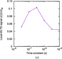
These three samples were scanned on a 1.5 × 1.5 µm2 area with a resolution of 30 × 30 pixels and analyzed by the proposed local-DLTS method (Fig. 17). By analyzing the acquired images, the time constant τ and the magnitude of transient capacitance response were obtained at each pixel. Figure 17(a) shows a typical local-DLTS spectrum obtained for #S-45-1. We reconstructed the transient capacitance response (C–t curve) from the spectrum, as shown in Fig. 17(b) with its raw data. Both C–t curves fit well with each other. Thus, it was confirmed that the local-DLTS spectrum well reproduces the capacitance response. Figure 18 shows images of local-DLTS signals at approximately τ = 1 µs. The highest brightness was obtained from #S-45-1 and the lowest one from #S-45-3, which is consistent with the macroscopically obtained result. Furthermore, in the local-DLTS images, we detected dark and bright areas, which indicate the two-dimensional trap distribution.
Download figure:
Standard image High-resolution image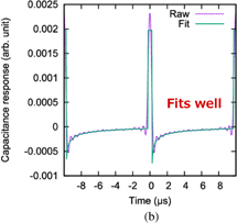
Fig. 17. (a) Local-DLTS spectrum measured on S-45-1 sample. (b) Reconstructed and raw capacitance responses (C–t curves).
Download figure:
Standard image High-resolution image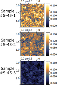
Fig. 18. Images of local-DLTS signals at approximately t = 1 µs in SiC MOS interface. The dark and bright areas indicate low-Dit (trap density) area and high-Dit area, respectively.
Download figure:
Standard image High-resolution imageNext, quantitative imaging of Dit by local-DLTS was performed. Figure 19 shows the distributions of Dit for τ = 0.3 and 3 µs. Assuming the capture cross section to be 10−16 cm2, the time constants 0.3 and 3 µs correspond to the energy depths of 0.24 and 0.30 eV below the conduction band, respectively. The average Dit values in Fig. 19 are of the same order of magnitude as Dit values at the corresponding energy level measured by the macroscopic high-low method. All images have dark and bright areas with a feature size of 100 nm. In addition, the images with different time constants showed different distributions, which implies that the distribution of interface traps depends on the time constant or that the physical origins of interface traps with different energy levels are different. Thus, we conclude that this local-DLTS technique can contribute to the understanding of two-dimensionally distributed microscopic physical properties of the MOS interface.
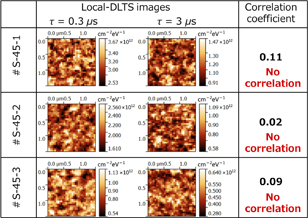
Fig. 19. 2D distribution of Dit converted from local-DLTS signals for τ = 0.3 and 3 µs.
Download figure:
Standard image High-resolution image10. Atomic-resolution measurement of semiconductor surface by noncontact SNDM and proposal of scanning nonlinear dielectric potentiometry
In the SNDM technique, we detect the capacitance Cs of a very small portion of a specimen immediately under the conducting tip of the SNDM probe. Cs varies with time because of the nonlinear dielectric response under the applied alternating electric field E3 (= Ep cos ωpt).
Equation (4) is a polynomial expansion of the electric displacement D3 as a function of the electric field E3 just under the tip.

Here, Ps3 is spontaneous polarization, and ε2, ε3, and ε4 are the linear, lowest-order nonlinear, and higher-order nonlinear dielectric constants, respectively.
The even-rank tensors, including ε2 and ε4, are insensitive to the state of spontaneous polarization. In contrast, ε3 is very sensitive to the spontaneous polarization Ps3. For example, there is no ε3 in materials with a center of symmetry, such as an isotropic material, and the sign of ε3 changes with the inversion of spontaneous polarization. Thus, by detecting ε3 microscopically, we can measure the distribution of polarization.
The ratio of this derivative capacitance variation ΔCs occurring just under the metal tip to the static capacitance Cs is given by

Here, the alternating capacitance of different frequencies corresponds to each order of the nonlinear dielectric constant. Signals corresponding to ε3 and ε4 are obtained by setting the reference signal of the lock-in amplifier of the SNDM system to a frequency equal to ωp and 2ωp of the applied electric field, respectively.
A new technique called NC-SNDM has been proposed to increase the resolution of SNDM.8) By operating SNDM in the noncontact mode, the resolution degradation caused by tip abrasion can be prevented, and a higher resolution can be achieved. As shown in Fig. 20, NC-SNDM employs the localized higher-order nonlinear dielectric signal, i.e., the ε4 signal (the second term on the right-hand side of Eq. (5) with the doubled frequency 2ωp of the applied alternating bias voltage frequency ωp) for the control of the noncontact state (tip–sample gap control), and the simultaneous detection of the localized lowest-order nonlinear dielectric signal, i.e., the ε3 signal [the first term on the right-hand side of Eq. (5) with the same frequency ωp] for the detection of polarization. Thus, in the noncontact mode, NC-SNDM can simultaneously detect the topography and polarization (electric dipole moment in atomic-scale measurement) distribution. The ε4 signal is highly suitable for maintaining the tip–sample distance constant for noncontact control, because it does not depend on the polarity of the dipole moment and the penetration depth of this signal into the sample is much smaller than that of the ε3 signal.
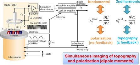
Fig. 20. Schematic diagram of NC-SNDM.
Download figure:
Standard image High-resolution imageWe have recently developed an NC-SNDM system operated in ultrahigh vacuum to prove that NC-SNDM has real atomic resolution. Figure 21 shows the probe for NC-SNDM operated in ultrahigh vacuum and its outer appearance. Unlike the contact-type SNDM probe using the cantilever tip, the probe tip of NC-SNDM is an all-metal needle just like an STM tip. Using this NC-SNDM, we have succeeded in observing the Si(111)7 × 7 atomic structure. The result is shown in Fig. 22. Atomically resolved topography and the atomic dipole moment have been simultaneously obtained.9) Figure 22(a) shows the topography obtained from the up-and-down motion of the piezo z-stage when the higher-order nonlinear dielectric signal (ε4 signal) was used as a feedback signal for ε4 to be constant. Figure 22(b) shows the simultaneously acquired lowest-order nonlinear dielectric ε3 signal image, which is thought to correspond to the distribution of atomic dipole moments. In this case, a dc bias voltage of −0.5 V was applied between the tip and the sample to emphasize the contrast of adatoms. A positive dipole moment was detected on the Si adatom sites, whereas a negative dipole moment was observed at the interstitial sites of inter-Si adatoms. Upon bias voltage application, the head of dipole moments in interstitial sites of Si adatoms is switched to the negative direction. At this point, under a bias voltage of −0.5 V, the average value of the polarization of the Si(111) surface becomes almost zero by the cancellation of positive and negative dipole moments. A comparison between Figs. 22(b) and 22(a) clearly reveals a single positive dipole moment detected at the adatom site indicated by arrows in the figure. The adatom site is composed of top positive adatom Si nuclei and negative electrons making up the covalent bonds just below the adatom; thus, the dipole moment direction at this site is upward. On the other hand, a negative dipole moment was observed at the interstitial sites of inter-Si adatoms. This is the first successful demonstration of the atomic resolution of a dielectric microscopic technique.

Fig. 21. Probe for NC-SNDM operated in ultrahigh vacuum and UHV NC-SNDM outer appearance.25)
Download figure:
Standard image High-resolution image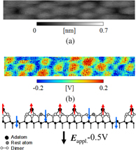
Fig. 22. (a) Topography obtained from the higher-order nonlinear dialectic signal (ε4 signal) of Si(111) 7 × 7 structure (b) Simultaneously obtained lowest order nonlinear dielectric ε3 signal image (dipole moment image).25)
Download figure:
Standard image High-resolution imageMoreover, by extending this NC-SNDM method, we have developed a new SNDP that can measure dipole-moment-induced surface potential with atomic resolution.19) In this method, bias voltage is fed back to cancel the ε3 signal, which means that we apply bias voltage until we recover the symmetry of the system broken by an electric dipole moment. As mentioned above, ε3 is very sensitive to the spontaneous polarization or permanent dipole moment Ps3, so when apparent total Ps3 is canceled by the dipole moment induced by the bias voltage application, ε3 correspondingly becomes zero. Thus, the voltage applied to cancel ε3 corresponds to the dipole-induced potential. Specifically, for quantitative discussion, see Ref. 19.
Figure 23 shows the operation principle of SNDP. SNDP is only sensitive to polarization- or dipole-induced potentials, unlike Kelvin probe force microscopy (KPFM), which cannot distinguish the contributions from the contact potential difference, fixed monopole charges, and spontaneous polarization.19) By SNDP, we simultaneously measured the topography and surface potential of a graphene monolayer formed on a 4H-SiC(0001) substrate. For example, a result is shown in Fig. 24. Very small benzene circles (six-membered carbon rings) and a relatively large sixfold moire pattern with the potential distribution induced by dipole moment in the interface between the graphene monolayers and the 4H-SiC(0001) substrate are clearly visualized20) in the figure in which the topography and potential image are overlaid.
Fig. 23. Schematic diagram of SNDP.
Download figure:
Standard image High-resolution image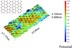
Fig. 24. Observation of interfacial charge state of graphene monolayer on 4H-SiC(0001) substrate. Potential image is overlaid on the topography.25)
Download figure:
Standard image High-resolution image
11. Conclusions
In this paper, we reviewed the high-resolution characterization of fine structures of semiconductor devices and materials using SNDM and its extended versions. First, the principle of SNDM was described, in which the mechanism underlying the high sensitivity of the order of 10−22 F/ was revealed. Also, characterization results for some semiconductor devices were introduced. Then, many newly developed SNDM methods (SHO-SNDM, local-DLTS, NC-SNDM, and SNDP) were briefly introduced and their applications to the characterization of several semiconductor devices and materials were described.
The good measurement results indicate that SNDM and its extended methods are very powerful tools for the measurement of semiconductor devices and materials.
Acknowledgment
This work was supported in part by a Grant-in-Aid for Scientific Research (S) (No. 16H06360) from the Japan Society for Promotion of Science (JSPS).
Biographies

Yasuo Cho graduated in 1980 from Tohoku University in electrical engineering department. In 1985 he became a research associate at Research Institute of Electrical Communication, Tohoku University. In 1990, he received an associate professorship from Yamaguchi University. He then became an associate professor in 1997 and a full professor in 2001 at Research Institute of Electrical Communication, Tohoku University. During this time, his main research interests included nonlinear phenomena in ferroelectric materials and their applications, research on the scanning nonlinear dielectric microscopy (SNDM), and research on using the SNDM in next-generation ultrahigh density ferroelectric data storage (SNDM ferroelectric probe memory).