
Abstract
Liquid phase crystallization has emerged as a novel approach to grow large grained polycrystalline silicon films on glass with high electronic quality. In recent years a lot of effort was conducted by different groups to determine and optimize suitable interlayer materials, enhance the crystallographic quality or to improve post crystallization treatments. In this paper, we give an overview on liquid phase crystallization and describe the necessary process steps and discuss their influence on the absorber properties. Available line sources are compared and different interlayer configurations are presented. Furthermore, we present one-dimensional numerical simulations of a rear junction device, considering silicon absorber thicknesses between 1 and 500 µm. We vary the front surface recombination velocity as well as doping density and minority carrier lifetime in the absorber. The simulations suggest that a higher absorber doping density is beneficial for layer thicknesses below 20 µm or when the minority carrier lifetime is short. Finally, we discuss possible routes for device optimization and propose a hybride cell structure to circumvent current limitations in device design.
Export citation and abstract BibTeX RIS
1. Introduction
With a cumulative installed capacity of 177 GWP1) photovoltaics (PV) delivers a reliable share of electricity generation. Today, the dominant technology is silicon wafer PV with energy conversion efficiencies of crystalline silicon (c-Si) solar cells exceeding 25%.2,3) The price learning curve for PV (see, e.g., Ref. 4) illustrated that the economy of scale caused a reduction in price by a factor of 10 within the last decade. This makes PV available to a wide range of applications from small roof-top installations up to utility-scale. In order to be cost competitive in the future, efforts are made to further reduce the wafer thickness. A thickness reduction below 100 µm would require revolutionary new concepts and cannot be reached by evolutionary developments in the current c-Si based PV industry. Beside the demand to save material to reduce cost, the high specific energy consumption for silicon production gives raise for novel disruptive approaches to generate solar energy.
Life cycle analysis performed in Ref. 6 illustrate that silicon wafer PV exhibits almost three times higher greenhouse gas (GHG) emission and specific energy consumption compared to other technologies for utility scale PV. Comparing the results of Ref. 6 with an older study from 20057) shows that the remarkable efficiency increase of the silicon wafer modules did not change this situation significantly. The specific silicon demand of 4.5 g W which is likely to saturate due to wafering and handling restriction accounts for the majority of energy consumption and GHG emission up to 72% of the specific emission for a PV module6,7) during production. Life cycle analysis attribute silicon wafer PV a specific greenhouse gas emission of about 180–190 kg m−2.6) Beside these emissions it was shown by Fthenakis et al.8) that also nitrogenous-oxide and sulfur-oxide emissions of silicon wafer PV manufacturing are higher than for thin-film technologies. In order to reduce these specific emissions the specific silicon consumption per Watt has to be reduced drastically while maintaining a high conversion efficiency of the cells. To illustrate the material and energy saving potential of thin-film crystalline silicon Table I estimates the energy demand for feedstock, crystallization, wafering and cell processing as well as encapsulation for two imaginary wafer based cases with the liquid phase crystallization approach. The wafer based cases assume novel wafering methods or an alternative feedstock technology. The c-Si case assumes silicon from the Siemens process and ion implantation as a kerfless technology for wafering. The wafers are 40 µm thin. Polycrystalline silicon (poly-Si) assumes polycrystalline material that was fabricated using an alternative feedstock technology (40% less energy than for the c-Si case) and 120 µm thin wafers. The wafering method for this case assumes a technology which uses 25% less energy than ion implantation. The available data was taken from Ref. 5 and included references. For device preparation, a generic hetero-junction device concept was assumed. It should be noticed that a high number of processes were not considered in Table I. However, as it can be seen from the table, liquid phase crystallized silicon on glass offers a significant reduction of the specific energy demand even for a low conversion efficiency of 15%. Depending on the technologies used for feedstock preparation and wafering the energy demand for the presented wafer cases ranges from 393 MJ m−2 up to 408 MJ m−2 which is almost 3 times higher than the energy demand for LPC-Si. This illustrates the potential of thin crystalline silicon on glass. However, silicon based thin film technologies were intensively investigated in the past years to offer an alternative technology to wafers based on abundant and non-toxic materials. The most promising technology, amorphous- and microcrystalline tandem devices demonstrated conversion efficiencies close to 13%9) and large scale production. However, as this technology is not able to fulfill the cost requirements of the mass market, its share is decreasing continuously. Main limitations of this technology were the electronic quality of the microcrystalline bottom cell on one hand, and on the other hand the limited short circuit current density of the amorphous top-cell. Circumventing these limitation caused increased complexity of the device due to need for intermediate reflectors, textured glasses or high mobility TCOs etc. Alternative technologies based on poly-Si on glass were intensively developed but never transferred to a sustainable business model. As a rule of thumb high electronic quality requires large and defect free crystals,10) that require high temperatures that are not compatible with glass substrates. Different techniques were applied to solve this problems including solid phase crystallization,11–15) aluminium-induced crystallization,16–18) as well as seed-layers combined with epitaxial thickening.19,20) Unfortunately, all methods exhibited limitations with respect to the maximum achievable open-circuit voltage (VOC) below 500 mV combined with a maximum absorber thickness of a few micrometers. Recently, liquid-phase crystallization (LPC) of silicon by means of zone melting using continuous wave (cw) diode lasers or electron beams showed very promising results21–23) with VOC values above 650 mV.24–26) With LPC, the main limitation of VOC below 600 mV was overcome and current LPC-Si absorbers enable VOC values that are comparable to results achieved using conventional multi-crystalline silicon (mc-Si) wafer cells, i.e., 664 mV with a 100-µm-thick mc-Si wafer.27)
Table I. Comparison of the energy demand for liquid phase crystallized silicon with two imaginary wafer based approaches. Raw data of selected processes were taken from Ref. 5 and included references.
| c-Si | poly-Si | LPC-Si | |
|---|---|---|---|
| Wafer thickness (µm) | 40 | 120 | 10 |
| Conversion efficiency (%) | 21 | 19 | 15 |
| Ingot yield (%) | 81 | 80 | 80 |
| Wafering yield (%) | 98 | 98 | 98 |
| Kerfloss (%) | 0 | 70 | 0 |
| Cell processing yield (%) | 99 | 99 | 80 |
| Feedstock (MJ m−2) | 63.7 | 114 | 16.1 |
| Crystallization (MJ m−2) | 29.2 | 19.6 | 2.3 |
| Wafering energy (MJ m−2) | 189 | 162.7 | 0 |
| Cell processing (MJ m−2) | 44.5 | 44.5 | 55.6 |
| Encapsulation (MJ m−2) | 66.7 | 66.7 | 66.7 |
| Total energy demand (MJ m−2) | 393 | 408 | 140 |
2. Liquid phase crystallization
Liquid phase crystallization has emerged as a zone melting technology to grow high-quality thin poly-Si films on glass. A huge amount of research on thin-film zone melting was performed in the 1980s and 1990s (see, e.g., Refs. 28 and 29) for 3D integration in microelectronics or solar cells on high temperature substrates.30,31) As no high energy density line sources were available, graphite strip heaters32) or focused halogen lamps33) were used. The lack of energy rendered the use of high scanning speeds impossible. Heat loss to the substrate was severe and only high temperature stable materials such as graphite, silicon, quartz or oxide-/nitride ceramics were used. In order to achieve scanning speeds in the cm s−1 range a preheat temperature up to 1300 °C is neccessary32) that is not possible with glass. To meet the requirements of fast scanning speeds, continuous wave high density energy sources have to be used such as diode lasers or electron beams. This marks a significant difference to the zone melting experiments mentioned above. A sketch illustrating the present approach of liquid phase crystallization of silicon layers on a glass substrate is given in Fig. 1.
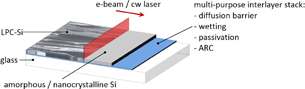
Fig. 1. Sketch of the LPC approach of silicon on a glass substrate.
Download figure:
Standard image High-resolution image2.1. Line sources
The availability and price drop of semiconductor lasers made it possible to create line length of several centimeters. Using diodes that emit at a wavelength of 808 nm a power density of 3000 W/cm2 and higher is achievable which is sufficient to crystallize with scanning speeds of cm s−1. An alternative to semiconductor lasers are line-shaped electron beams that are simple to build and operate but require vacuum. As demonstrated in Ref. 21 acceleration voltages up to 8 kV and emission current densities of 10 mA per centimeter line length are sufficient to melt silicon on glass up to 40 µm in thickness and with a scanning speed up to 20 mm s−1. Higher scanning speeds are possible for both sources but as shown in Ref. 21 the amount of grain boundaries is increased if the scanning speed exceeds 20 mm s−1 for a 10 µm thin silicon film. Comparing the advantages and disadvantages of these energy sources, laser sources feature a self limiting process as the reflectivity of the silicon increases as soon as the material is liquid. Thus, the amount of energy introduced is reduced until resolidification, resulting in a high process stability. Furthermore, if the crystallization process is performed in an oxygen containing atmosphere no capping layer is necessary to prevent dewetting of the film. The major disadvantage of diode lasers is the limited lifetime of the diodes and the large absorption depth in silicon that makes these sources inefficient for silicon thicknesses well below 5 µm. In addition, if the sample exhibits glass faces that are not coated with silicon, no absorption takes place and no heat is generated in these areas which causes a high amount of stress and an increase of cracking probability of the glass substrate.
For electron beam based systems21) the major disadvantage is the necessity for vacuum. Here, if crystallization is not performed on an amorphous or microcrystalline silicon carbon layer (SiCx), a dedicated capping layer is needed in order to prevent the molten silicon from forming droplets.34) Furthermore, evaporating silicon can coat the focusing electrodes and glow cathode and therefore destabilize the process. As the electrons are fully absorbed in liquid and solid silicon, no self limitation of the process is achievable. Advantageous is that uncoated glass is also heated and stress inside the substrate is significantly reduced. Due to the low acceleration voltage used in Ref. 21, electron beam induced liquid phase crystallization is well suited for crystallizing very thin layers of silicon between 100 nm up to 1 µm.
2.2. Glass, interlayer and process stability
The application of liquid phase crystallization for PV energy generation requires the usage of commercially well available and cheap substrates. Up to now, LPC was successfully applied to borosilicate glass (Borofloat 33)23,25,35) or alumo-boro silicate glasses (Corning Eagle XG)24,36,37) that are commonly used for flat panel display fabrication. High thermal endurance as well as a silicon matched thermal expansion coefficient make these glasses an ideal substrate. After cleaning, an interlayer stack is deposited on the substrate. This interlayer material or stack between glass substrate and silicon is the most important part of the device to achieve high electronic quality. The interlayer has to meet different requirements. First, it has to act as mechanical buffer and diffusion barrier as impurities enclosed in the substrate will diffuse into the silicon during crystallization. Second, the interlayer has to act as wetting promoter for the silicon film during melt. Third, the material of the stack in direct contact with the silicon has to provide a high level of surface passivation. This is mandatory as this interface is not accessible after crystallization. Fourth, if used in superstrate configuration for solar cells or sensors, anti-reflective properties are necessary. And finally, depending on the absorber deposition process, it has to act as a dopant layer for the silicon.
In early experiments only a single layer was deposited on the glass, that was later replaced by stacks containing silicon-carbide, -nitride, or -oxide or recently aluminiumoxide.38) Siliconcarbide is the best choice in terms of wetting.21,39) It provides a large energy range for crystallization without causing the silicon to delamintate. However, it is only a poor diffusion barrier against common glass impurities and causes high surface recombination.34) SiCx was thus replaced by silicondioxide as an efficient diffusion barrier against common glass impurities such as boron, aluminium or iron. In addition it provides a high level of interface passivation,40) but the wettability of silicon is significantly reduced. An extra capping layer might have to be deposited on top of the silicon before crystallization to maintain a stable process. As shown by Ref. 41 the level of surface passivation provided by silicondioxide is sufficient for superstrate devices. Further increase in electronic quality was achieved by Dore et al.39) integrating an additional silconnitride layer as anti-reflective coating (ARC). To maintain the high level of surface passivation a second silicon dioxide layer was added. So far sputtered ONO stacks allowed for conversion efficiencies close to 12% for n- and p-type material.35,36) For sputtering, reactive RF-magnetron processes were used successfully by different groups.23,34) As no hydrogen is introduced during the process, substrate temperatures as low as 150 °C can be used. A promising alternative for p-type silicon is a triple stack replacing the silicon nitride layer by aluminiumoxide38) due to the excellent surface passivation properties.
If low-temperature plasma-enchanced CVD (PECVD) is used for interlayer deposition, a subsequent high temperature annealing has to be performed to reduce the amount of hydrogen inside the interlayer to avoid delamination during crystallization due to rapid effusion of incorporated hydrogen. A comprehensive comparison and description of the development steps for PECVD interlayers was performed by Gabriel et al.25) It should be noticed that in Ref. 25 a commercial PECVD system (Applied Materials AKT 1600A) was used to deposit suitable interlayers for LPC on 30 × 30 cm2 substrates.
After interlayer deposition the silicon absorber is deposited in an amorphous or nanocrystalline form by means of high-rate electron beam evaporation,23,35,36) low-pressure CVD (LPCVD)21) or PECVD.25,42) Doping is provided in-situ or by the deposition of an additional silicon layer by means of PECVD or sputtering from a highly doped target. Afterwards the sample is crystallized by preheating the substrate to a steady temperature around 600 °C and subsequently scanning the energy source over the substrate. Figure 2 shows the relationship of power and energy during crystallization for laser induced LPC in atmosphere (data taken from Ref. 37). As sketched in Fig. 2, the minimum power necessary to crystallize a silicon absorber is a function of the scanning speed. The onset of longitudinal grain growth is shown by the blue line. Below this threshold power, the silicon is only partly molten causing grain growth perpendicular to the scanning direction. Grain sizes in this region are a few micrometers up to 20 µm in diameter. As soon as the threshold level is exceeded, the silicon is completely molten and the grain growth occurs parallel to scanning direction. If the power level is increased further and exceeds the upper limit (black curve in the figure) the layer will peel off. As shown in Fig. 2, the usable process window becomes smaller with increasing scanning velocity. If we refer to the energy dose displayed in Fig. 2 right, we can see the convergence of the energy necessary for longitudinal grain growth. As shown by the curve, the amount of energy increases significantly with lower scanning speeds, underlining that a large amount of the energy is lost by heat conduction to the ambient and the substrate. This heat loss is reduced for scanning speeds as high as 6 mm s−1. The selected scanning speed has a strong influence on the possibility to form cracks in the crystallized layer or the substrate. As the heat loss for low scanning speed causes the glass surface to soften and thus reduce thermal stress by plastic deformation, the surface stays rigid for high scanning speed and residual stress is stored by elastic deformation released by cracking (Fig. 2 right).
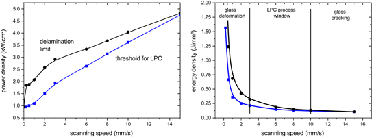
Fig. 2. Power density (left) and energy density (right) for liquid phase crystallization with respect to the applied scanning speed (threshold for LPC (blue), delamination limit (black). Data taken from Ref. 37.
Download figure:
Standard image High-resolution image2.3. Morphological properties of LPC absorbers
Due to the directional solidification, liquid phase crystallized absorbers exhibit a grain structure comparable to wafers formed by the edge defined film fed growth43) (EFG) or string-ribbon44) method. The morphology is dominated by longitudinal grains that extend up to cm in length and a few millimeters in width. As shown by EBSD cross sections, the grains extend through the whole layer thickness12) thus the photo generated carriers are not exposed to grain boundaries when passing through the absorber. Usually the grains are randomly oriented but recently, as shown by Kühnapfel et al.37) a (100) preferential orientation can be achieved if the power chosen for crystallization is near the threshold level for longitudinal growth (blue curve in Fig. 2). If the power level is increased well above this level, the morphology is not changed in terms of crystal size, but the grain orientation becomes random. As shown in Ref. 37, independent of the crystallization power used, the grain orientation in scanning direction is (101).
2.4. Impurities and electronic quality
In order to investigate the suitability of the interlayer as diffusion barrier, and to study the bulk quality of the silicon, different methods were used including secondary ion mass spectroscopy (SIMS),12,23) electron beam induced current (EBIC),45) photoluminescence (PL),34,46–48) electron paramagnetic resonance (EPR),49) or analysis of the internal quantum efficiency (IQE).24,38) A detailed study of the electronic quality of LPC-Si absorbers was performed in Ref. 45 using EBSD, EBIC as well as PL using a single layer of silicon carbide as interlayer. It was found that the average diffusion length of the material is in the order of the thickness of the absorber, but significantly reduced to values below 1/10th of the thickness in areas with a high dislocation density. These electrically dead areas are formed preferably at cracks inside the silicon and extend over the whole surface of the sample and are usually 100–300 µm wide (see Fig. 3). Compared to other poly-silicon absorbers on glass such as solid phase- or pulse laser crystallized silicon, LPC absorbers exhibit a pronounced 1.1 eV band-to-band recombination signal using PL and only minor contribution of defect luminescence at 0.8 eV.46)

Fig. 3. LBIC survey of a solar cell with liquid phase crystallized absorber. Homogeneous LBIC signal within grains, no LBIC response in regions with high dislocation density (blue circles).
Download figure:
Standard image High-resolution imageHowever, as determined in Ref. 45 the SiCx:Si interface exhibits strong surface recombination velocity exceeding 106 cm s−1. Furthermore, EPR measurements of the dangling bond density49) revealed a trap density in the order of several 1015 cm−3. A comparison of IQE data of samples crystallized on SiCx with samples that were processed on silicon dioxide23) revealed a significant reduction in IQE if silicon carbide is used as interlayer. For crystallization on SiCx a maximum value of 0.5 was determined, on SiO2 a value of 0.9 was measured. A comparison of different interlayer materials with respect to the open-circuit voltage conducted by Dore et al.39) showed that even if the silicon carbide is coated with an additional oxide (OCO), a reduction in VOC of about 50 mV is observed compared to SiO2. Samples crystallized on ONO interlayers did not show a reduction in open-circuit voltage compared to a single SiO2 layer. However, depending on the preparation of the silicon nitride layer, a change in VOC around 15 mV was observed.39) Another study on the influence of the interlayer on the electronic quality was performed by Haschke et al.41) The comparison of the open-circuit voltages of test cells on n- and p-type absorber revealed that the SiNx layer in the ONO stacks is beneficial to the open-circuit voltage. As shown in Ref. 41 a boost in VOC up to 30 mV is achieved if single SiO2 is replaced with ONO for n- as well as p-type absorbers with different doping levels. This indicates that the silicon nitride layers with the amount of build in charges causes a field passivation of the absorber and the silicon dioxide is acting as dielectric. This would also explain the influence of the thickness of the final silicon oxide layer or SiO2 contact layer on the open-circuit voltage.38)
For n-type absorbers the optimum SiO2 contact layer thickness was determined to 5 nm.38) If crystallization is performed on silicon nitride, or on SiO2 contact layers that are 10 nm or thicker the open-circuit voltage is reduced by 19 mV (crystallization on silicon nitride) or 14–17 mV (10 and 15 nm SiO2). Furthermore, the open-circuit voltage for n-type silicon was found to be significantly higher than for p-type. Independent of the absorber doping level, n-type silicon exhibits VOCs that are 40 mV higher on average than p-type material.41) For p-type silicon on silicon oxide/aluminium oxide/silicon oxide it was found that the influence of the SiO2 contact layer thickness is not as pronounced as for n-type on ONO and no significant difference was found between 5 and 10 nm thick SiO2 as contact layer.38)
A detailed investigation of the difference between n- and p-type poly-Si was performed by Ref. 50 with respect to the morphological and electronical quality. The samples used in this study were grown by high temperature CVD up to a thickness of 10 µm and characterized using Fourier transform infrared spectroscopy (FTPS), electron spin resonance (ESR), TEM, and Suns–VOC measurements. Furthermore, the influence of hydrogen passivation was investigated. N- and p-type absorber exhibited a dangling bond density of 1.8 × 1017 cm−3 (p-type) and 2.6 × 1017 cm−3 (n-type) that can be reduced by a factor of 3.5 to 5.7 (p-type) and 3.7 to 4.5 (n-type) using hydrogen passivation. As described in the paper no advantage of n-type silicon over p-type material was found. Therefore it should be feasible to achieve the same level of open-circuit voltage for p-type LPC-silicon. Recently, a VOC of 612 mV was demonstrated on p-type LPC-Si51) on PECVD interlayers. Hall measurements of polycrystalline absorbers yielded that carrier mobilities close to values for mono crystalline silicon are achievable: For p-type material, a hole mobility up to 400 cm2 V−1 s−1 was reported52) on a single grain. If the contacts enclose multiple grains, hole mobilities up to 200 cm2 V−1 s−1 were reported51) for p-type and for n-type electron mobilities up to 800 cm2 V−1 s−1 at dopant concentration in the upper 1016 cm−3 range.
3. Device considerations
Due to the high temperatures during liquid phase crystallization, a rear junction back contact system might be the contact system of choice for LPC-Si solar cells on glass. In this section, first, a simulation study is presented: the absorber properties are varied for a rear junction device to shed light on the different requirements and optimum configurations when reducing the thickness of the silicon absorber to values far below 100 µm. A similar study has been presented by Kowalczewski et al.53) However, they focussed on p-type material, a front junction device and minority carrier lifetimes not shorter than 15 µs. Later, present device approaches are reviewed and discussed with respect to their limitations. Finally, suggestions for an optimal device architecture for LPC-Si material are outlined.
3.1. Simulation study: Rear junction silicon solar cells — from wafers to thin films
3.1.1. Numerical model.
The one-dimensional numerical device simulations were carried out using the device simulator AFORS-HET,54) which has been developed at Helmholtz–Zentrum Berlin. For the calculation of the generation rate, the Lambert–Beer model has been used which allows for multiple passes of the light through the semiconductor stack. The external reflection has been set to zero (Rext = 0), the internal reflection at front- and back-contact boundaries to one (Rint = 1) and an optical path length enhancement of 10 has been assumed. With this, a photo current density jPh = 32.2 mA cm−2 is generated in a 2.2-µm-thick silicon absorber which is close to the experimentally demonstrated short circuit current density jSC = 29.5 mA cm−2 for such a silicon absorber.11) As such, the simulation assumes a good, but not unrealistic light trapping. For the electrical modelling of the n-type silicon absorber the "c-Si model" included in the program has been used. Auger recombination has been considered using the model of Kerr and Cuevas.55) Hence, the only free parameters for the description of the silicon absorber are the doping density ND and the defect concentration at midgap Ntr. The doping dependency of the mobilities are considered by the program according to Masetti et al.56) As the simulations presented here shall demonstrate the influence of the absorber properties, the a-Si:H(p) hole contact has been modelled highly idealized. That is: (i) without any defects, to avoid a limitation of the VOC due to these defects, and (ii) with sufficiently high doping [NA = 1016 cm−3, leading to a difference of 238 meV between the conduction band and the valence band in the a-Si:H(p)] so that also for the theoretical case of a surface recombination velocity of 0 cm s−1 at the front side, the open-circuit voltage equals the splitting of the quasi Fermi levels and is not limited by insufficient selectivity of the contact.
3.1.2. Simulation of illuminated j(V)-parameters.
In Fig. 4, the illuminated j(V)-parameters VOC, jSC, and the efficiency (η) are plotted versus the absorber thickness of a rear junction silicon hetero junction (SHJ) solar cell with an n-type absorber. In the simulation the surface recombination velocity of the front side Sfront has been varied from 0 to 1000 cm s−1, and the simulations have been performed for two different absorber base doping densities: a moderate doping density where ND = 1016 cm−3 and a high doping density with ND = 1018 cm−3. Additionally, two different defect concentrations Ntr have been considered: a low defect concentration Ntr = 109 cm−3, which corresponds to a minority charge carrier lifetime in a "high quality silicon wafer" (τSRH = 10 ms) and an elevated defect concentration Ntr = 1013 cm−3 which corresponds to a Shockley–Read–Hall (SRH) lifetime of τSRH = 1 µs, a typical value for LPC-Si material obtained from fitting the EQE with numerical one dimensional simulations.24) The j(V)-parameters for the "long lifetime case" are depicted on the left hand side of Figs. 4(a), 4(c), and 4(e) and for the "short lifetime case" on the right hand side (b), (d), and (f). For specific absorber thicknesses, the generated photo current density is denoted on the upper x-axis.
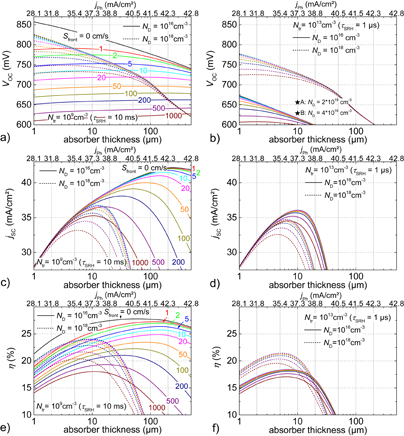
Fig. 4. Illuminated j(V)-parameters VOC, jSC, and η for a rear junction silicon heterojunction solar cell obtained using one-dimensional numerical device simulation. The parameters are plotted versus the thickness of the silicon absorber and have been calculated for two doping densities ND and two defect densities Ntr. Left: "long lifetime case" (τSRH = 10 ms), right: "short lifetime case" (τSRH = 1 µs). The VOC values marked with a star in (b) are experimentally obtained values taken from Ref. 24.
Download figure:
Standard image High-resolution imageIn the "long lifetime case" and with moderate doping (ND = 1016 cm−3) the open-circuit voltage is mainly a function of the surface recombination velocity at the front side Sfront. In the considered range of absorber thickness for Sfront < 100 cm s−1, a maximum of the VOC is observed that shifts towards thinner absorber thicknesses for lower Sfront. For the theoretical case of Sfront = 0 cm s−1, VOC constantly rises in the investigated range. In general, the VOC equals the splitting of the quasi Fermi levels, if sufficiently high charge carrier selectivity at the contacts is provided. In that case, the VOC is only dependant on the excess charge carrier density Δp for a given doping concentration. With this, the observed characteristic of the maxima can be explained by two opposing effects that both affect Δp. On one hand, there is an increase in Δp due to the enhanced generation rate with decreasing absorber thickness leading to a higher VOC. On the other hand, with decreasing absorber thickness, recombination at the front side is more effective as the front side is moving closer to the excess charge carriers inside the absorber. The higher Sfront, the sooner this effect outweighs the higher Δp in thinner absorbers. For Sfront = 0 cm s−1, the second effect does not occur, hence the VOC is solely increasing towards thinner absorbers. With a higher doping concentration ND inside the absorber, the quasi Fermi level of the majority carriers is shifted closer to the conduction band edge and thus enables higher open-circuit voltages. However, intrinsic Auger recombination is increasing with increasing doping. At ND = 1016 cm−3, intrinsic recombination after Kerr and Cuevas55) τKC is limiting the effective lifetime τeff to about 1.5 ms (at Δp = 1015 cm−3). Due to the logarithmic relation between VOC and lifetime, the influence on the VOC is still relatively low at this lifetime level. Unlike for ND = 1018 cm−3, where τeff is limited to 10 µs due to intrinsic recombination and thus limiting the maximum achievable VOC as can be seen in Fig. 4(a). For this reason, higher doping enables a higher VOC as long as the effective lifetime is not limited by intrinsic Auger recombination. This is particularly the case for absorber material with a shorter SRH minority carrier lifetime (τSRH) or for high surface recombination velocities. This is emphasized when looking at the results for the "short lifetime case" in Fig. 4(b). The SRH lifetime τSRH is 1 µs and hence at ND = 1018 cm−3 still shorter than τKC. The result is that at ND = 1018 cm−3 the VOC is following basically the same trend for both the long as well as the short minority carrier lifetime in the absorber, while for τSRH = 1 µs the VOC is generally between 50 and 100 mV lower due to the reduced SRH lifetime. Note that in the "short lifetime case" for the moderate doping density of ND = 1016 cm−3, the VOC is generally 100 mV lower compared with the values of the highly doped absorber.
Due to the fact that the minority charge carriers are collected at the side averted from the sun, the front surface recombination velocity is strongly affecting the short circuit current density jSC. It is worth noting, that for decreasing absorber thicknesses, a higher Sfront can be accepted. As an example, for a 200-µm-thick absorber with ND = 1016 cm−3 and τSRH = 10 ms, a front surface recombination velocity of 100 cm s−1 is reducing the generated photo current density jPh of 42.3 mA cm−2 to a short circuit current density of 36.4 mA cm−2. In this case jSC is about 86% of jPh. For a 50 µm thick absorber with the same properties, jSC (39.1 mA cm−2) amounts to 97% of jPh (40.5 mA cm−2). The use of thinner absorber layers hence lowers the requirements for the passivation of the front side in matters of the jSC.
While higher doping can enable higher VOC, depending on (i) absorber thickness, (ii) bulk minority carrier lifetime and (iii) recombination velocity at the front side, a higher doping density will generally lead to a lower jSC due to the reduced mobility. Referring to the efficiency in Figs. 4(e) and 4(f), the higher VOC due to higher doping overcompensates the reduced jSC and leads to higher efficiency, especially for thin absorbers (<20 µm), shorter minority carrier lifetimes in the bulk, and elevated front surface recombination velocities. Additionally, a two-dimensional device like an interdigitated back contact solar cell would benefit from higher doping in terms of majority carrier transport, which becomes increasingly important when going to thinner absorber layers and thus reduced lateral conductivity. Note though, that for a two-dimensional device, the requirements on the diffusion length can be higher than in the one-dimensional case that has been considered here.
3.2. General considerations regarding the device architecture
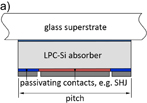
The one-dimensional rear junction device discussed in the previous section cannot be easily applied to LPC-Si absorber material due to the difficulties of both-side contacting. With a two-dimensional device architecture, however, additional design restrictions have to be considered. Due to the thin absorber, lateral transport is limited as compared with classical wafer thicknesses in the range of 150–200 µm. However, the pitch [cf. Fig. 5(a) for definition] needs to be smaller to account for the reduced conductivity. Ke et al. report on an optimal pitch of 570 µm for a 10-µm-thick silicon absorber,57) while it is in the millimeter range for wafer based IBC devices.58–60) With the use of high doping and n-type absorber material the conductivity is increased, alleviating this problem. Another issue is the reduced diffusion length in LPC-Si material. With diffusion lengths in the range of 10–30 µm24,48) for state of the art material the width of the absorber contact should be kept as small as possible to reduce electrical shading, i.e., the loss of minority charge carriers that are generated above the absorber contacts due to recombination. For short diffusion lengths in the absorber material itself, this will happen even if the silicon surface at the contact is well passivated. However, so far, the specific contact resistivity of passivating contacts is generally greater than 100 mΩ cm2 61–63) thus requiring large contact fractions in order not to limit current transport. As sketched in Fig. 5, this is compulsorily lowering the area fraction of the contact that is collecting the minority charge carriers. However, it has already been demonstrated that in principle, for current LPC-Si material charge carrier collection can benefit from absorber contact passivation.64)
Download figure:
Standard image High-resolution image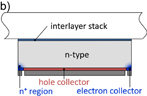
Fig. 5. Schemes of possible device structures. a) passivating contacts for both polarities, e.g., silicon heterojunction contacts. b) Hybrid structure with a passivating minority contact (hole collector in the case of an n-type absorber) and small area electron contacts, e.g., realized with localized n+ regions, to allow for very low-ohmic contacts.
Download figure:
Standard image High-resolution image
3.3. Review of existing device approaches
Up to now, several approaches have been followed to build solar cell devices on LPC silicon absorber material.23,24,65–68) For the formation of the carrier selective minority contact, diffused23,66) as well as heterojunctions24,65,68) have been used, while the majority contacts are often realized using a direct metal contact.23,65,66) All approaches have in common that they rely on single side contacting. The most relevant results with respect to achieved conversion efficiency are rear junction devices and listed in Table II. The approaches differ with respect to the formation of the selective contacts and their form. The highest efficiency reported so far is 12.1% and has been achieved using a 11 µm n-type absorber with a relatively high doping density of 9 × 1016 cm−3.42) The minority contact is formed with a SHJ, while the majority charge carriers are extracted via direct metal contacts. Although using an insulation layer65) the device structure resembles the one of interdigitated back contacts (IBC). Structuring has been realized using photolithography and shadow masks. Other approaches35,67) rely on industrially more relevant structuring techniques, using a similar contacting scheme as was used by former company CSG solar,69) which relies on inkjet printing and laser structuring. Here, the absorber is contacted via point contacts. Except for the result presented by Dore et al.,35) the efficiency of the devices is stable as the crystalline absorber material does not suffer from light induced degradation. Regarding the LPC devices with VOC values above 600 mV, the main limitation for higher efficiency is a low fill factor (FF) which does not exceed 70% for all devices presented in Table II. In the respective references, different reasons for the low FF are given, ranging from high contact resistivity at the absorber contacts24) over cracks in the absorber42) to restricted transport across the a-Si:H(p)/ITO layer stack.67)
Table II. Overview of current LPC devices based on p- and n-type absorber material, using different contacting schemes and structuring techniques.
| Contacts | Absorber | VOC (mV) | jSC (mA cm−2) | FF (%) | η, Ref. (%) | ||
|---|---|---|---|---|---|---|---|
| Minority | Majority | Doping | Structuring | ||||
| Diff. | Metal | p-type | Laser and inkjet | 585a) | 27.6 | 72.4a) | 11.7a), 35 |
| SHJ | SHJ | n-type | Photolithogr. | 612 | 30.3 | 57.0 | 10.5, 68 |
| SHJ | Metal/diff. | n-type | Laser | 619 | 28.2 | 65.6 | 11.5, 67 |
| SHJ | Metal | p-type | Photolithogr. | 618 | 29.4 | 64.8 | 11.8, 42 |
| SHJ | Metal | n-type | Photolithogr. | 649 | 27.3 | 68.4 | 12.1, 42 |
a) Not stable over time.
We would like to emphasize that the development of a cost efficient and industrially producible contacting scheme is not straightforward for LPC-Si on glass and one of the key challenges for this approach.
3.4. Discussion of the efficiency potential
In a recent publication,41) we projected a mid-term efficiency potential of 16%. Given the current market situation and the efficiency level of standard technology, this may not be sufficient to be competitive. Without profound cost analysis it is difficult to pronounce whether LPC-Si solar cells will be competitive with standard waferbased technologies. However, we still would like to discuss the possibilities for the optimization of VOC, jSC, and FF in this section.
3.4.1. Open-circuit voltage.
In general, the cause of the high VOC (above 600 mV24,26,41,42)) values is not fully understood yet. Looking at Table III it may be suggested that high VOC stems from the use of a silicon heterojunction as passivating minority contact, as the only device in Table III with a VOC below 600 mV features a diffused minority contact. However, we suppose that rather the interplay between doping type and passivation at the absorber/interlayer interface plays the major role in the determination of the VOC. This is supported by the fact that all reported LPC-Si devices with a p-type absorber and SiOx as the layer in contact with the silicon surface feature VOC values below 600 mV.35,36,66) This could be explained by the fact that, especially at high doping densities, for p-type silicon the surface recombination velocity at the Si/SiO2 interface is much higher than for n-type silicon.70) This might not be the case for a p-type silicon surface passivated with SiOxNy, which could be the reason behind the VOC of 618 mV recently obtained by Frijnts et al. using a p-type absorber on an NO(ON) barrier stack.42) Calnan et al. conducted a detailed study on different interlayers71) and state that the addition of nitrogen to SiOx could lower the interfacial strain and consequently enhance surface passivation.
Table III. Overview of VOC values of solar cells based on LPC-Si. Given in the table are potentially VOC-influencing parameters such as the doping type and density of the absorber, the materials of the interlayer (stack), and the contacts. Barrier nomenclature as follows: O: SiOx, N: SiNx, ON: SiOxNy.
| Absorber | Barrier type | VOC, Ref. (mV) | ||||
|---|---|---|---|---|---|---|
| Contacts | Doping type (cm−3) | Thickness (µm) | ||||
| Minority | Majority | |||||
| SHJ | Metal | n-type | 1 × 10¹⁷ | 6.5 | N | 567, 66 |
| SHJ | Metal | p-type | 4 × 10¹⁶ | 10 | O | 577, 36 |
| Diff. | Metal | p-type | 8 × 10¹⁵ | 10 | ONO | 585, 35 |
| SHJ | Metal | p-type | 6 × 10¹⁶ | 7.5 | NO(ON) | 618, 42 |
| SHJ | Metal/diff. | n-type | 3 × 10¹⁶ | 10 | NON(ON) | 619, 67 |
| SHJ | Metal | n-type | 9 × 10¹⁶ | 11 | NO(ON) | 649, 42 |
| SHJ | Metal | n-type | 2 × 10¹⁸ | 10 | ONO | 656, 24 |
Regarding further device optimization, it is difficult to determine what is limiting the VOC of current LPC-Si devices as at this stage both interfaces (the SHJ and the one between the absorber and the interlayers) as well as the lifetime in the absorber itself could limit VOC. This can be nicely seen from the experimental data point of device B included in Fig. 4(b). The τSRH of device B was estimated to be at least 1 µs in an earlier publication.24) However, despite the higher generation rate assumed in the simulation, for τSRH = 1 µs and at 10 µm thickness only 617 mV are obtained for the simulated rear junction device, compared to 629 mV of the experimental device B. The difference in VOC of about 10 mV could be explained by different scenarios: (i) τSRH in device B is actually longer than 1 µs. Assuming e.g., 2 µs would allow for such high VOC. Still, τSRH could be even higher and VOC determined by Sfront. (ii) the higher VOC could be also primarily enabled by the higher doping density of device B. This underlines the difficulty to give exact numbers for absorber lifetimes. However, for device A (ND = 2 × 1018 cm−3), the VOC is much lower than would be expected from the simulation given that the same τSRH = 1 µs could be reached as for device B. So it can be stated that τSRH seems to be reduced due to the higher doping as we suggested already in an earlier publication.41)
Given that τSRH of 1 µs could be obtained also at a doping density of ND = 1018 cm−3 VOCs close to or even above 700 mV might be possible for absorber thicknesses in the range of 10 µm, as suggested by the simulations shown in Sect. 3.1.2.
3.4.2. Short circuit current density/light trapping.
It is commonly known that the thinner the thickness of an indirect semiconductor material such as silicon the higher the importance of excellent light trapping to absorb as much sunlight as possible. To realize that, monocrystalline (100) silicon wafer material is usually wet-chemically textured (using KOH) with random pyramids on both sides which is providing pronounced light scattering. At the back side, a stack of a non-absorbing dielectric such as e.g., SiO2 and a metal like e.g., silver can provide a high level of internal reflection with almost no parasitic absorption. The dielectric acts as an optical spacer, decoupling the metal from the interface to avoid absorption of the evanescent waves within the metal.72) Ideally, the refractive index of the optical spacer should be as close as possible to one and its absorption coefficient should be zero to avoid absorption of both evanescent as well as propagating waves within the material.72) In the case of an IBC-SHJ generally a TCO is used as an optical spacer.2,73) While the application of such layers to LPC-Si devices is easy, the texturing of the interfaces is more difficult, as the surface of the LPC-Si is not necessarily a (100) oriented surface, mandatory for random pyramid texturing. First experiments to obtain a preferential growth leading to a (100) orientated LPC-Si surface have been reported by Kühnapfel et al.37) In principle, also approaches to texture multicrystalline silicon74,75) could be applied, although the preparation of well passivating SHJ contacts may be difficult on such surfaces. The texturing of the interface of silicon and the glass is especially important to reduce the reflectivity. However, the implementation of light scattering features at this position is challenging as silicon surface passivation and crystal growth during LPC must not be deteriorated. With nanoimprint glass, in principle excellent light scattering can be achieved,76) however, depending on the imprinted structure, the material quality can be strongly reduced by stress induced structural defects.77) Whether this could be reduced by directly texturing the glass as for instance described in Refs. 78 and 79 is ongoing research. It is worth mentioning that with the use of a capping layer (cf. Sect. 2 and Ref. 36), the texture of the glass can be preserved also at the silicon surface averted from the glass.76) With this, a double-side texture can be obtained without any further process steps, independently from surface orientation.
For a high short circuit current density, however, also efficient carrier collection is needed. The most easy way to achieve this would be that the fraction of the minority collecting contact is as large as possible which is accompanied by potential limitations regarding the fill factor as will be discussed in the following section.
3.4.3. Fill factor.
One important question is if the device structure for the currently highest efficiency for a silicon solar cell2) i.e., the interdigitated back contact silicon heterojunction (IBC-SHJ) is also the optimal device structure for the LPC-Si absorbers on glass. Especially as with current material quality, large fractions of the minority collecting contact are needed, hence, only little space is available for the majority contact. As already mentioned, with most passivating contacts, contact resistances are currently above 100 mΩ cm2,61–63) which would already induce 1 Ω cm2 assuming an absorber contact fraction of 10%. Therefore, we suggest that a hybrid structure may be more suited at the current level of absorber material quality. In such a structure we suppose that a small absorber contact fraction (<5%) with low contact resistance is realized with local diffusion, or a direct metal contact (both e.g., laser fired) is used while the bigger part is covered with a passivating minority contact e.g., formed using a SHJ or the approach using a thin passivating oxide.63,80) With advancing absorber quality this may be revisited again.
4. Summary and outlook
It was shown that thin poly-Si films on glass offer a great potential to significantly reduce the amount of energy necessary to produce PV modules on the one hand and save a large amount of silicon and therefore cost of PV on the other. Considering the composition of the European power generation the total greenhouse gas emission of PV can be strongly reduced using absorber thicknesses well below 40 µm. The availability of line sources with high power densities enable zone melting of silicon on substrates with only limited thermal stability such as glass. Scanning speeds in the range of cm s−1 results in macroscopic grains of the absorber that allow for the application of a variety of processes known from wafer based PV. As the electronic quality is defined during crystallization one can choose the absorber deposition technique only with respect to throughput and efficiency. Combined with the usage of direct line sources this results in a cheap and scalable technology. Sputtered as well as PECVD interlayers were developed by different groups that resulted in wafer equivalent material properties on borosilicate or alumo-boro silicate glasses. For liquid phase crystallized silicon on Schott Borofloat or Corning Eagle XG, it was shown that oxygen and carbon inside the crystallized layers is on Czochralsky wafer level and electron mobilities up to 800 cm2 V−1 s−1 can be achieved. One possible route to further improve the material quality was shown by Kühnapfel et al. by growing layers with (100) preferential orientation. This would allow to use simple KOH-based texturing in a very efficient way to enhance light trapping. Finally first steps were taken to grow monocrystalline layers including seed-layers at the beginning of the crystallization process. This would open novel applications in large area microelectronics or sensors.
Regarding possible photovoltaic devices, using higher doping densities for thin silicon absorber layers can enable higher VOC values as well as higher efficiencies, especially when the lifetime in the absorber is limited. Particularly, the doping density should be increased as long as intrinsic recombination is not limiting the effective lifetime in the absorber. In the current material, however, high n-type doping in the range of 1018 cm−3 not only increases intrinsic recombination, but also SRH recombination compared with a moderately doped absorber (4 × 1016 cm−3).
A device in rear junction configuration will benefit from thinner absorber layers as the requirements for the passivation of the front side are lower. While the surface recombination velocity at the front side should be below 10 cm s−1 for a 100-µm-thick absorber, it can be 100 cm s−1 for a 10-µm-thick absorber without deteriorating current collection.
With respect to current absorber quality, we suggest that an IBC-SHJ is not the device architecture of choice, as it is difficult to obtain a passivating low-ohmic absorber contact. Instead, we propose to use a hybride structure with a large minority contact fraction and an absorber contact fraction below 5%. This proposal will change with further improvements of minority carrier lifetime in the absorber.
Acknowledgment
The authors gratefully acknowledge the support of E. Conrad, C. Last, A. Opitz, M. Wittig, and M. Reiche in solar cell preparation. T. Hänel and K. Mack are acknowledged for support in measuring.
Appendix: Simulation details
The simulations shown in Sect. 3.1.2 were carried out using AFORS-HET v2.4.1.54) The parameters to model the semiconductor layers are summarized in Table A·1. Please note that AFORS-HET v2.5 has been released only recently, including e.g., tunneling transport.81)
Table A·1. Parameters used in the one-dimensional simulations performed with AFORS-HET.
| c-Si absorber | |
| Bulk model | c-Si |
| Thickness w (µm) | 1 to 500 |
| Electrical band gap Eg (eV) | 1.124 |
| Electron affinity χ (eV) | 4.05 |
| Doping density ND (cm−3) | 1016, 1018 |
| Midgap trap density Ntr (cm−3) | 109, 1013 |
| a-Si:H(p) hole collector | |
| Bulk model | Standard |
| Thickness w (nm) | 10 |
| Electrical band gap Eg (eV) | 1.72 |
| Electron affinity χ (eV) | 3.9 |
| Acceptor density NA (cm−3) | 1016 |
| Electron mobility μn (cm V−1 s−1) | 60 |
| Hole mobility μp (cm V−1 s−1) | 15 |
| No traps | |