

Abstract
Effective light trapping is essential for improving the efficiency and reducing the cost of thin-film silicon solar cells. Here, we numerically study the optical characteristics of periodic three-dimensional (3D) silicon nanocavity arrays. We found that the 3D silicon nanocavity array shows low sensitivity to geometric structural parameters for photon capture and achieves an outstanding efficiency superior to those of previously reported silicon nanostructures such as a nanowire and a nanohole with the same thickness. This excellence is attributed to a better antireflection capability and more resonant modes. The 3D silicon nanocavity array provides a new light-trapping strategy for thin-film photovoltaic devices.
Export citation and abstract BibTeX RIS
Over the past years, the market for solar power has been growing fast and the market-dominating solar panels are made from silicon because of its excellent lifetime, high reliability, and high natural abundance.1) In order to make solar power sufficiently competitive with fossil fuels, there is a strong drive towards the development of thin crystalline silicon solar cells that allow for dramatically reduced material usage, short carrier diffusion lengths, and high-efficiency operation.2,3) However, the weak absorption in the near-infrared part of the solar spectrum limits the efficiency of thin crystalline silicon solar cells. Recently, nanophotonic and plasmonic structures have been proposed as effective light trapping strategies to improve the sunlight absorption of thin silicon films.4–8) Significantly enhanced photon capturing capability has been theoretically and experimentally demonstrated on silicon nanostructures including nanowires,9–12) nanoholes,13–15) nanocones,16–19) and nanofunnel arrays.20,21) However, the absorption spectra of these light-trapping nanostructures show strong dependence on the geometric structural parameters. This presents a challenge to the machining technology and simultaneously increases the cost.
In this work, we used a finite-difference time-domain (FDTD) method to numerically investigate the optical characteristics of regularly arranged three-dimensional (3D) silicon nanocavity arrays on thin-film silicon in the solar spectrum. It is found that the 3D silicon nanocavity array shows low structural parameter sensitivity for photon capture, which is attributed to its better antireflection capability and more supported resonant modes. Moreover, the 3D silicon nanocavity array shows significantly enhanced absorption that exceeds those of the previously reported arrays.
Figure 1(a) schematically illustrates the 3D silicon nanocavity arrays on silicon. Solar irradiation is directly incident on to the top of the nanostructure along the z-direction. The side- and top-view images of a single 3D silicon nanocavity are shown in Figs. 1(b) and 1(c), respectively. The 3D silicon nanocavity array consists of a cuboid middle part, pyramidal bottom part, and octagonal-pyramid top part. The period of the square lattice is defined as P, the diameter at the upper surface of the 3D silicon nanocavity is D1, and the width of the middle part is D. The heights of the top part, middle part, and bottom part of the array are L1, L2, and L3, respectively. The filling factor is  , which is defined as the unit cell area occupied by the octagon on the surface area. The periodic boundary conditions are applied in the simulation. X is the double length between the side of the octagonal surface and the side of the square lattice. In our analysis, the thickness of the 3D silicon nanocavity array L is fixed at 2.33 µm. This value is comparable to the thickness of silicon thin-film solar cells22,23) and allows a comparison with the results in a previous report.11,13,20) Such 3D silicon nanocavity arrays can be readily fabricated by lithography and metal-assisted chemical etching of crystalline silicon and subsequent etching in alkaline solution. Therefore, the angle between the facet of the pyramid and the surface is 54.7°.24) The relationships among the various structural parameters among the 3D silicon nanocavity arrays are given by


Fig. 1. (a) Schematic illustration of the 3D silicon nanocavity arrays. (b) Side view and (c) top view of a single array.
Download figure:
Standard image High-resolution imageAs can be concluded from the above equations, the 3D silicon nanocavity arrays are characterized by L2, L3, and X. The underlying physics on determining the optical structural parameters is clarified.
The overall light absorption performance of the array is evaluated using ultimate efficiency η defined as
Here, I(λ) is the spectral energy density at AM 1.5G, λ is the wavelength, λg is the wavelength corresponding to the silicon bandgap, and A(λ) is the absorption. To calculate η, it is assumed that each photon with energy greater than the silicon band gap would be absorbed and the recombination processes of electron–hole pairs are not considered.
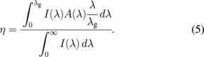
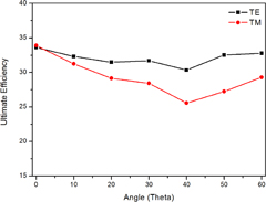
Figure 2(a) shows the ultimate efficiency of 3D silicon nanocavity arrays at different lengths L2 and we chose a fixed f = 0.75 as a representative in the simulation. The ultimate efficiency of the arrays remains high with increasing length L2 in a wide range and achieves a maximum of 33.36% when L2 is 1.63 µm. Figure 2(b) shows the absorption spectra of 3D silicon nanocavity arrays for the five representative points indicated in Fig. 2(a) and also shows the calculated absorption of 2.33 µm planar silicon for comparison. The absorption of the arrays is significantly enhanced across the whole solar spectrum, especially in the long-wavelength region (>0.8 µm). The absorption of the 3D silicon nanocavity arrays decreases in the short-wavelength range as L2 > 1.63 µm. We suggest that the 3D silicon nanocavity with increasing length L2 in this range would be very similar to the square nanohole, which has been proved to be less efficient in light absorption.25) It should be noted that the 3D silicon nanocavity arrays exhibit high light absorption in the near-infrared part of the solar spectrum, and the ultimate efficiency also shows low sensitivity to L2 over a wide range.

Download figure:
Standard image High-resolution image
Fig. 2. (a) Ultimate efficiency and (b) wavelength-dependent absorption spectra of the 3D silicon nanocavity arrays at different lengths L2.
Download figure:
Standard image High-resolution imageFigure 3(a) shows the ultimate efficiency of the 3D silicon nanocavity arrays at different lengths L3. Although the ultimate efficiency varies with L3 changes, but it still remains in a high range, exceeding 29%. The balance between the reflection and transmission spectra leads to the high absorption. Herein, we choose L2 = 1.03 µm as a representative value to further investigate the influence of L3 on light harvesting. Figures 3(b)–3(d) show the absorption, reflection, and transmission spectra of the points circled in Fig. 3(a), respectively. In Fig. 3(b), the absorption is significantly enhanced owing to the addition of 3D silicon nanocavity arrays in the silicon thin film. In addition to the light absorption enhancement in the short-wavelength range, the 3D silicon nanocavity arrays also show efficient absorption in the long-wavelength range. It is also interesting to note the similar absorption spectra, reflection spectra, and transmission spectra of the arrays with various L3 as shown in Figs. 3(b)–3(d), respectively. Therefore, we can conclude that the high ultimate efficiency of the 3D silicon nanocavity arrays shows relative low sensitivity to the length L3.
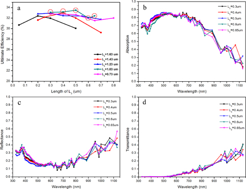
Fig. 3. (a) Ultimate efficiency of the 3D silicon nanocavity arrays as a function of length L3. (b) Absorption, (c) reflection, and (d) transmission spectra of the structure with different lengths L3.
Download figure:
Standard image High-resolution imageFigure 4(a) shows the ultimate efficiency of 3D silicon nanocavity arrays at different filling fractions. The maximum ultimate efficiency of the arrays reaches 34.38% at L2 = 1.63 µm and f = 0.875. The efficiency is higher than previously reported ultimate efficiencies of SiNW26) and SiNCH21) array counterparts. The insets show the electric fields of the 3D silicon nanocavity, SiNW, and SiNCH arrays under the wavelength of 827 nm. High transmission in SiNW arrays and weak absorption in SiNCH arrays lead to poor ultimate efficiency compared with the 3D silicon nanocavity. The absorption properties of 3D silicon nanocavity arrays with different filling fractions are calculated and shown in Fig. 4(b). More peaks can be observed for 3D silicon nanocavity arrays with increasing filling fraction especially in the long-wavelength range, indicating that more resonant modes maybe supported. The insets show the electric field distribution of the arrays with f = 0.875 and 0.444 at the wavelength of 827 nm. The result further confirms the additional resonances with increasing filling fraction. In addition, the more gradual change of the effective refractive index of the arrays along the z-axis direction also results in better antireflection and thus leads to the enhancement of optical absorption. Figure 4(d) shows the effective refractive indices of 3D silicon nanocavity arrays as a function of the thickness when L2 = 1.63 µm. The effective refractive index of the arrays is described as the average refractive index between air (n = 1) and silicon (n = 4.089) weighted by their volumes. The 3D silicon nanocavity arrays with f = 0.875 achieve the most gradual change in the effective refractive index along the z-axis direction and show the best optical absorption property. The result is consistent with the absorption and reflection spectra shown in Figs. 4(b) and 4(c) where the absorption of the 3D silicon nanocavity arrays increases and the reflection decreases with increasing filling fraction, especially in the short-wavelength range. The transmission of the 3D silicon nanocavity arrays for all the filling fractions is nearly zero in the short-wavelength range, further confirming the effective antireflection characteristic of the arrays.
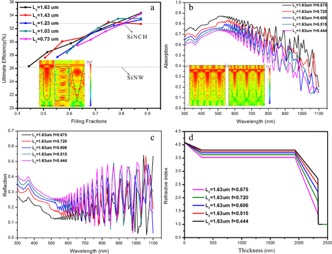
Fig. 4. (a) Ultimate efficiency of the 3D silicon nanocavity arrays at different filling fractions. The ultimate efficiencies of SiNW and SiNCH are shown for comparison. (The insets show the electric fields of the 3D silicon nanocavity, and SiNW and SiNCH arrays under the wavelength of 827 nm.) (b) Absorption (insets show the electric fields of the arrays under the wavelength of 827 nm when f = 0.875 and 0.444). (c) Reflection spectra of the structure at different filling fractions. (d) Effective refractive indices of the 3D silicon nanocavity arrays as a function of thickness.
Download figure:
Standard image High-resolution imageAll the simulations above were performed with normal incident light. However, for practical photovoltaic device applications, the incident angle of the sunlight must be taken into consideration because of the relative motions of the sun and the earth. We calculated the ultimate efficiencies of 3D silicon nanocavity arrays as a function of the angle from the surface normal for TE and TM polarizations at L2 = 1.63 µm and f = 0.875, as shown in Fig. 5. It can be seen that the 3D silicon nanocavity array shows a high ultimate efficiency even at incident angles up to 60°. The slightly increase in the ultimate efficiency after 40° may be due to the absorption increase in the long-wavelength range.
Fig. 5. Calculated ultimate efficiencies of 3D silicon nanocavity arrays as a function of the angle from the surface normal for TE and TM polarizations at L2 = 1.63 µm and f = 0.875.
Download figure:
Standard image High-resolution image
In conclusion, the optical properties of regularly arranged 3D silicon nanocavity arrays were studied in detail. Our calculation results indicated that the light-trapping capability of the 3D silicon nanocavity arrays shows low sensitivity to geometric structural parameters and maintains high ultimate efficiency over a broad range reaching a maximum of 34.38%. Better antireflective performance, more supported resonances modes and enhanced resonance mode interaction contribute to the significantly enhanced light absorption of the array. The low sensitivity of the arrays for efficient light harvesting reduce the complexity of the fabrication process and thus save on cost. The 3D silicon nanocavity arrays provide a promising light-trapping strategy for high-performance thin-film photovoltaic devices.
Acknowledgments
We acknowledge financial support from NSFC (51072025, 91333208), National Basic Research Program of China (2012CB93220), Beijing Nova Program (2008B24), and the Fundamental Research Funds of the Central Universities (2012LZD02).