

Abstract
The lowest resistivity of highly Si-doped Al0.62Ga0.38N was achieved using metalorganic vapor epitaxy. The resistivity strongly depended on the Si concentrations and reached a minimum value of 6.6 × 10⁻³ Ω cm at a Si concentration of 3.2 × 1019 cm−3, where the carrier concentration was close to the Si one. Above this concentration, luminescence bands around 2.4 eV originating from group-III-vacancy–Si complexes (VIII–nSi) were observed, whereas carrier concentrations and mobilities decreased. Growth conditions that avoid high temperatures and V/III ratios result in suppressed formation of VIII–nSi, playing a key role in achieving low resistivity.
Export citation and abstract BibTeX RIS
Aluminum nitride (AlN) and aluminum gallium nitride (AlGaN) have ultrawide bandgaps and are key materials for the next generation of high-power electronic devices and deep ultraviolet (UV) light sources. Instead of traditional bulky low-pressure mercury lamps, AlGaN-based deep UV light emitting diodes (LEDs) are expected to be utilized in applications such as purification, sterilization, disinfection of medical instruments, and UV curing. Recent reports indicate that external quantum efficiencies (EQEs) over 10% were achieved for deep UV LEDs, with the emission wavelengths around 280 nm.1–4) However, further improvements in EQEs are required for high-power applications because the large power losses lead to an increase in device size and the reduction of reliability due to heating during operation. Additionally, an improvement in wall-plug efficiency (WPE) is also desired to replace mercury lamps. The WPE is generally reduced by some loss components as follows: the non-radiative recombination in quantum wells,5) the absorption loss through a p-type contact layer,6,7) the hole injection loss from a p-type side,8) and the electron injection loss due to the series resistance of n-type AlGaN (n-AlGaN). The reduction in the last-mentioned series resistance of n-AlGaN layers has been studied for application to UV LEDs with Al-rich n-AlGaN cladding layers.9–14)
There are two possible sources for increasing the resistance of an n-AlGaN layer. First, in the high AlN mole fraction n-AlGaN, a silicon (Si) atom no longer plays as a shallow donor due to the emergence of a DX state with the increase of the AlN mole fraction, resulting in increasing ionization energies.15) The wide range of ionization energies for DX states in AlN and AlGaN have been reported to be within 78 to 345 meV.10,16–20) The second source is the self-compensation effect due to the complexes between cation vacancies–silicon (VIII–nSi) complexes.21) Bryan et al.12) indicated that VIII–nSi complexes were responsible for a high Si doping limit above 2 × 1019 cm−3 in Al0.7Ga0.3N layers and enhanced for samples with higher dislocation densities. Suppression of such compensation sources could significantly improve the conductivity of high AlN mole fraction n-AlGaN layers.22,23) In addition, the correlation between electron mobility and the concentration of self-compensation sources has been identified and can play a key role in resistivity control.12) To realize low-resistance n-AlGaN, it is also necessary to understand this suppression of self-compensation by controlling the growth conditions. In the present study, we successfully demonstrate the lowest resistance of n-Al0.62Ga0.38N on sapphire substrates at the high Si doping of 3 × 1019 cm−3 with less carrier compensation. The optical and electrical characterizations suggest that the suppression of VIII–nSi formation by controlling growth condition plays a key role for reducing resistance. Additionally, we demonstrate the mobility degradation due to VIII–nSi complexes, which can significantly contribute to the resistivity in the high Si doping regime.
Crystals of the AlN templates were grown using low-pressure metalorganic vapor phase epitaxy (MOVPE). Trimethylaluminum (TMAl), trimethylgallium (TMGa), and ammonia (NH3) gas were utilized as Al, Ga, and N precursors, respectively. Monosilane (SiH4) was utilized as a Si dopant. The surface of a 4-in. c-plane flat sapphire substrate (FSS) with a misorientation angle of 0.35° was thermally cleaned in a hydrogen ambient, followed by the low-temperature (LT) growth of a 0.3-μm-thick AlN and the subsequent high-temperature (HT) growth of a 3 μm thick AlN at approximately 1200 and 1400 °C, respectively. These LT-AlN layers were grown as a nucleation layer to suppress cracking and relax stress intentionally by providing roughness on the surface and air voids in the templates, while the HT-buffer layer reduced the number of threading dislocations.24) Subsequently, 1.3 μm thick n-Al0.62Ga0.38N layers were grown on AlN templates, where the AlN mole fraction was set to be around 0.62 by adjusting a TMAl/TMGa ratio for each growth condition.
The crystalline structure of AlN templates was evaluated using high resolution X-ray diffraction measurements. The typical full width at half maximum (FWHM) value of the AlN template grown on the FSS was symmetric and single peaked; 200 and 320 arcsec for (002) and (102) diffractions, respectively. Based on the empirical equation,25) the corresponding screw and edge dislocation densities of the AlN template were estimated to be 9 × 10⁷ and 1 × 109 cm−2, respectively. No pits were observed on the surfaces of AIN templates. The FWHM values of the X-ray diffraction peaks of n-AlGaN layers were typically 300 and 355 arcsec for (002) and (102) diffractions, respectively. The screw and edge dislocation densities of the n-AlGaN layer were estimated to be 1 × 10⁸ and 9 × 108 cm−2, respectively. If an electron trap exists at every c-lattice translation along edge dislocations (i.e. one trap site per 0.25 nm),12,26,27) it can produce an electron compensation of 4 × 1016 cm−3 based on full trapping. This value of electron compensation may be overestimated if the occupancy of dislocation-related traps is less than unity, as is the case for a dislocation density of ∼109 cm−2, as indicated in Ref. 26. This indicates that carrier compensation due to threading dislocation is negligible in the high doping regime above 1018 cm−3. There were no obvious hillocks and no cracks on the surfaces of the n-AlGaN layers. The surface morphology of n-AlGaN layers featured three-dimensional islands with a root mean square roughness of 4–7 nm. The luminescence properties for n-AlGaN layers were examined using a cathodoluminescence (CL) system equipped with a scanning electron microscope (SEM) with the use of an acceleration voltage of 5 kV and a probe current of 1 nA at RT. These Si concentrations of the n-AlGaN layers were estimated by quadrupole type secondary ion mass spectrometry (SIMS), where the quantitative values were determined using a reference Al0.62Ga0.38N sample injected with Si-ions. Resistivities, carrier concentrations, and mobilities of the n-AlGaN layers were evaluated using the van-der-Pauw method and the Hall-effect measurement at RT. To perform these analyses, 7.5 mm square Hall devices were prepared by depositing 0.6 mm diameter Ti/Al/Ni electrodes at four corners. These electrodes were annealed at 700 °C in a nitrogen atmosphere. The I–V curves between the electrodes were linear. In addition, as the resistance between the electrodes of Hall devices is proportional to the sheet resistance, contact resistance is negligible in Hall-effect measurements.
We summarized the AlN mole fraction dependence of resistivity in n-AlGaN, including our results and those of other studies, as shown in Fig. 1.9–14,28–36) The lowest resistance of n-AlGaN with an AlN mole fraction of 62% was achieved in this study. The lowest resistivity value of the Al0.62Ga0.38N layer reached 6.6 × 10⁻³ Ω cm at the Si concentration of 3.2 × 1019 cm−3. When this n-AlGaN layer was applied to a UV emitter, no visible resistance loss at the n-type spreading layer was observed.
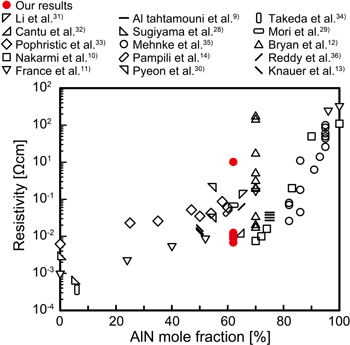
Fig. 1. (Color online) Resistivity values as a function of the AlN mole fraction for n-AlGaN layers. The data reported from other studies are indicated as open symbols,9–14,28–36) while our results are shown as red closed symbols.
Download figure:
Standard image High-resolution imageFigure 2(a) shows the Si concentration dependence of resistivity in n-AlGaN with an AlN mole fraction of 62%. The resistivity of the n-AlGaN layer decreased with increasing Si concentration, up to 3 × 1019 cm−3. The lowest resistivity of the n-AlGaN layer was doped at a Si concentration of 3 × 1019 cm−3. As Si atoms were further doped (>3 × 1019 cm−3), the resistivity increased extremely due to self-compensation. Figures 2(b) and 2(c) show the Si concentration dependencies of carrier concentration and mobility at RT, respectively. The correlation between carrier concentration and mobility is shown in the supplementary information (Fig. S1), available online at stacks.iop.org/APEX/13/025504/mmedia. The highest Si ionization ratio was 97% at 2 × 1019 cm−3 of Si concentration, indicating negligible carrier compensation. In the lower doping region (<2 × 1019 cm−3), the carrier concentrations nearly lay on the straight line of the 1: 1 relation for the majority of samples. The sample with carbon atoms of 4.4 × 1018 cm−3 close to the Si concentrations, as indicated by black arrows in Figs. 2(b) and 2(c), had a considerably lower carrier concentration than the Si one, which is possibly caused by electron compensation due to carbon on nitrogen site (CN) states. The corresponding sample also had an extremely lower mobility, owing to the impurity scattering by CN states. This feature agreed with the "mobility collapse", as reported by Kaess37) due to the ionized impurity scattering by carbon atoms. Moreover, both the carrier concentration and mobility dropped in the higher doping region above 3 × 1019 cm−3 due to the self-compensation effect.
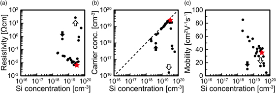
Fig. 2. (Color online) Si concentration dependence of (a) resistivity, (b) carrier concentration, and (c) mobility of n-type Al0.62Ga0.38N layers. The red star symbol shows the data of the lowest resistivity among n-type Al0.62Ga0.38N samples. The sample indicated by the black arrows involved a carbon concentration of 4.4 × 1018 cm−3 close to the Si concentration, while the other samples had at most a carbon concentration below 40% of the Si one. The white arrow indicates the sample that had a strong self-compensation effect because the carbon concentration was negligibly small compared to the Si doping concentration.
Download figure:
Standard image High-resolution imageTo clarify the compensation sources, CL analyses were performed for n-AlGaN layers fabricated by various growth conditions, as shown in Fig. 3. The CL spectra consisted of three luminescence bands: the near band edge (NBE) emission at the energy of 4.8–4.9 eV, which was close to the optical bandgap of Al0.62Ga0.38N,22) and two broad luminescence bands around 3.2 and 2.4 eV. Bryan et al.12) clarified that the 3.2 and 2.4 eV bands are attributable to a CN and VIII–nSi complexes, respectively. Based on this, the NBE and CN bands were dominant for all n-AlGaN layers with Si concentrations less than 3 × 1019 cm−3, as shown in Fig. 3(a). Above this doping range, the 2.4 eV band due to VIII–nSi complexes rapidly increased as the Si concentration increased, whereas the NBE and the 3.2 eV band were simultaneously reduced. Note that the rapid increase of the 2.4 eV band correlated to the increase in resistivity of high Si doping, as shown in Fig. 2, indicating carrier compensation due to VIII–nSi complexes. This trend is consistent with the previous report.12) For samples doped with a Si of 2 × 1019 cm−3, we also investigated the impact of the V/III ratio and growth temperature on the formation of VIII–nSi complexes as well as the 2.4 eV band. Figures 3(b) and 3(c) indicated that the formation of VIII–nSi was enhanced by the higher V/III ratio and the higher growth temperature. A temperature that is too high (1170 °C) leads to not only the increase of the 2.4 eV band, but also to the decrease in carrier concentration and mobility, as indicated by the white arrows in Figs. 2(b) and 2(c). Additionally, the V/III ratio of 1600 suppressed both the 3.2 and 2.4 eV bands, while enhancing NBE emission. In reality, the sample with the lowest resistivity was achieved using a V/III ratio of 1600, indicating that the optimal V/III ratio exists. These results provide a guideline towards the growth condition to suppress the formation of CN and VIII–nSi defects.
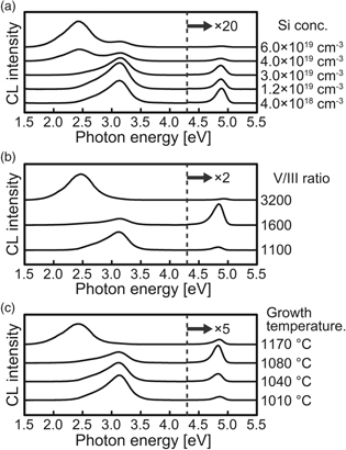
Fig. 3. (Color online) CL spectra for samples (a) with various Si concentrations, (b) grown with various V/III ratios, and (c) grown at different temperatures, where the indicated temperature was measured near the heater by thermocouple. Sample set (a) was grown with a V/III ratio of 1600 at 1010 °C. The Si concentration of sample sets (b) and (c) was set to around 2 × 1019 cm−3. Sample set (b) was prepared at 1040 °C, while set (c) was grown with V/III ratio of 1100. The NBE emission appeared around 4.8–4.9 eV. The 3.2 and 2.4 eV bands were caused by the recombination through the deep levels of CN and VIII–nSi complexes, respectively.12) The 1170 °C sample as shown in (c) corresponds to the sample indicated by the white arrow in Fig. 2. The dashed lines indicate the different standardization boundaries of the CL spectra. The spectra to the right side of the dashed lines are magnified as indicated.
Download figure:
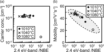
Standard image High-resolution imageTo investigate the correlation between VIII–nSi complexes and their electrical properties, carrier concentrations and mobilities were plotted as a function of the intensity ratio of the 2.4 eV band to the NBE for samples doped with Si of 2 × 1019 cm−3, as shown in Fig. 4. These data involve the samples used in Figs. 3(b) and 3(c). There were no significant changes in the carrier concentrations in the range of 2.4 eV–band intensity ratios below 20, indicating that the concentrations of the VIII–nSi defects were significantly lower than those of the shallow Si donors. However, gradual mobility degradation was observed with an increase in the 2.4 eV–band intensity ratio, suggesting ionized impurity scattering due to the VIII–nSi complexes. Moreover, the ionized-impurity-limited electron mobility is inversely proportional to the square of the number of charges (Z) in an ionized state.26) The Si donor is a single charge, whereas VIII–nSi complexes can take Z = 3 to 1 for n = 1 to 3.38) As the average Z value for VIII–nSi complexes is likely above unity, a complex can cause much stronger scattering than a single charged Si donor. This can explain the mobility degradation as the VIII–nSi concentrations increase, as shown in Fig. 4(b). Additionally, when the 2.4 eV–band intensity ratio is above a critical level, the carrier concentration abruptly dropped, as shown in Fig. 4(a). This can be explained by the majority of electrons being captured by the VIII–nSi acceptors, where the concentration of VIII–nSi complexes was likely closer to that of shallow donors. Consequently, the resistivity showed two trends: a gradual decrease due to mobility degradation and the abrupt drop due to compensation with the increase of the 2.4 eV–band intensity ratio. As described above, the suppression of VIII–nSi complexes evidently plays a key role in the resistivity control of n-AlGaN layers.
Fig. 4. (Color online) (a) Carrier concentration and (b) mobility for n-type Al0.62Ga0.38N layers as a function of the intensity ratio of 2.4 eV band to NBE in the CL spectra. The indicated temperatures were measured near the heater by thermocouples. The Si concentration of all samples was around 2 × 1019 cm−3. The n-AlGaN layers indicated by the different symbols were grown at different temperatures.
Download figure:
Standard image High-resolution image
In summary, we achieved the lowest resistance in n-AlGaN with an AlN mole fraction of 62%. The resistivity had a strong correlation with the formation of VIII–nSi complexes, which emerged as a 2.4 eV band in a CL spectrum. The key growth parameters to suppress the formation of VIII–nSi defects were clarified. We found that the increase in VIII–nSi concentration leads to mobility degradation due to ionized impurity scattering, even in the case of a VIII–nSi concentration significantly lower than that of the Si donors. Consequently, the suppression of the VIII–nSi complexes by control of the growth parameters is significant in a high Si doping regime for reducing the resistivity of Al-rich n-AlGaN layers. Because the dominant mechanism of resistivity increase likely depends on the AlN mole fraction, further investigations at different mole fractions are needed for applications to wider fields.