
Abstract
Combination of sputter deposition and high-temperature annealing is a promising technique for preparing AlN templates with a low threading dislocation density (TDD) at a lower film thickness compared to those prepared by the conventional metalorganic vapor phase epitaxy. However, cracking of AlN films during annealing is a critical issue. In this study, we controlled the residual stress of the sputter-deposited AlN films by modifying the sputtering conditions. Consequently, the occurrence of cracking was effectively suppressed. By optimizing the fabricating conditions, a TDD of 2.07 × 108 cm−2 was achieved for the AlN template with a thickness of 480 nm.
Export citation and abstract BibTeX RIS

Content from this work may be used under the terms of the Creative Commons Attribution 4.0 license. Any further distribution of this work must maintain attribution to the author(s) and the title of the work, journal citation and DOI.
Deep ultraviolet light-emitting diodes (DUV-LEDs) based on III-nitride semiconductors are expected to be applied in various fields for sterilization, disinfection, medical treatment, and curing.1,2) In order to realize DUV-LEDs with high efficiency and long-term reliability, it is essential to improve the crystalline quality of the AlGaN film which acts as a light emitting layer and an electrically conductive layer.3–5) Meanwhile, the crystalline quality of AlGaN is severely influenced by the crystalline quality of the underlying AlN buffer layer.6) Therefore, for improving the performance of DUV-LEDs, it is necessary to realize AlN templates with high crystalline quality on foreign substrates. Despite many research efforts for improving the quality of AlN on sapphire substrates, such as the modulation of the growth condition7–9) or epitaxial lateral overgrowth (ELOG) on patterned sapphire substrates (PSS),10–12) threading dislocation densities (TDDs) of the AlN films are still of the order of 108 cm−2. Typically, to eliminate the threading dislocations (TDs), it is necessary to grow a relatively thick AlN with a few-μm thickness via metalorganic vapor phase epitaxy (MOVPE) or hydride vapor phase epitaxy (HVPE) and make pair annihilation of TDs.13,14) Our group reported relatively high-quality AlN films with thicknesses less than 1 μm by performing high-temperature annealing.15) We could reduce the TDs in the as-grown AlN films via the solid state reaction during high-temperature annealing. Thus, there is no need to grow a thick AlN film for reducing TDs as is generally done with the conventional growth methods such as MOVPE or HVPE. Additionally, the combination of sputter deposition of AlN and the high-temperature annealing with face-to-face configuration (face-to-face annealing: FFA) leads to highly-uniform AlN films on large wafers at a low fabrication cost.16,17) A high-performance DUV-LED was previously demonstrated on the AlN template fabricated with this technique.18) However, there is a critical issue that cracks are likely to form in the AlN films during the high-temperature annealing.19) Because the thermal expansion coefficient (TEC) of sapphire is much larger than that of AlN,20,21) the sapphire substrate imposes enormous tensile stress on the AlN film when the temperature is increased. The occurrence of cracking stems from the tensile stress suffered by the AlN film during the heating sequence of the high-temperature annealing.22) We have already confirmed that reducing the annealing temperature or reducing the AlN film thickness are effective for suppressing the formation of cracks. Although, both these schemes are undesirable because the crystalline quality of AlN films after FFA will be degraded. Instead, for the suppression of cracking, we propose to accumulate the compressive residual stress and to increase the tolerance of AlN films to the tensile stress. In this work, we controlled the residual stress of sputter-deposited AlN films by modifying the pressure of the sputtering chamber (sputtering pressure). AlN films with various thicknesses were sputtered at various sputtering pressures. After high-temperature annealing, it was observed that both the sputtering pressure and the thickness of AlN films affected the tendency to crack and crystallinity of the films. Lastly, AlN films were grown on the annealed template by MOVPE and the surface morphology of the homoepitaxially grown AlN was investigated.
AlN films were deposited by radio frequency (RF) sputtering on c-plane sapphire substrates with a nominal surface off-cut angle of 0.2° with respect to m-axis. The diameter of the substrate was 2 inches. For RF sputtering, polycrystalline AlN was used as the source target. The background pressure of the sputtering chamber was lower than 6.0 × 10⁻⁵ Pa. N2 was supplied as the sputtering gas, and the amount of the supplied gas was 15–24 sccm. A series of AlN films with thicknesses ranging from 160 to 850 nm were fabricated under various sputtering pressures, from 0.03 to 0.4 Pa. During the AlN deposition, the substrate temperature and RF power were fixed at 600 °C and 700 W, respectively. After the deposition, high-temperature annealing was performed in the face-to-face configuration at 1650 °C–1775 °C under N2 ambient of 1013 hPa for 3 h.16) Unless otherwise mentioned, the typical annealing temperature used in this study was 1700 °C. Finally, AlN films were grown by MOVPE on the AlN templates fabricated by sputter deposition followed by FFA. For the MOVPE growth, trimethylaluminum (TMA) and ammonia (NH3) were used as precursors, and hydrogen (H2) was used as the carrier gas. The growth temperature, reactor pressure, and V/III element ratio were 1300 °C, 13 kPa, and 211, respectively. X-ray diffraction (XRD) was performed with an X-ray mirror and a channel-cut Ge(220) 2-bounce monochromator to characterize the crystalline quality and the lattice constants of the AlN films. The X-ray source was Cu, and Kα1 line (λ = 0.15406 nm) was used. A channel-cut Ge(220) 3-bounce analyzer was used for high-resolution X-ray rocking curve (XRC) measurements, and a one-dimensional semiconductor array detector was used for XRD reciprocal space map (XRD-RSM) measurements. The existence of cracks was checked with an optical microscope. Atomic force microscopy (AFM) was performed in the AC mode to investigate the surface morphology of the AlN films. Scanning transmission electron microscopy (STEM) characterization was performed to estimate the TDDs.
Before performing the high-temperature annealing, we investigated the residual stress of the sputter-deposited AlN films. Figures 1(a) and 1(b) show the a- and c-axis lattice constants, respectively, of the AlN films immediately after the sputter deposition. The lattice constants were evaluated by the XRD-RSM measurements from the AlN (10–15) diffraction. Considering the in-plane biaxial stress and elastic strain, a smaller (larger) a- (c-) axis lattice constant corresponds to compressive stress, while the opposite corresponds to tensile stress. There are some samples their both a- and c-axis lattice constants are larger than those of the bulk AlN,23) which means that unstrained lattice constants of sputtered AlN films are not equal to those of the bulk AlN. However, the relative magnitude of the residual stress can be evaluated from the results shown in Fig. 1. Upon comparing the samples with the same thickness, the AlN films deposited at a lower pressure are found to have a smaller a-axis lattice constant and larger c-axis lattice constant, which correspond to smaller tensile stress or larger compressive stress. In addition, in the case of a relatively high sputtering pressure, the tensile stress increases with the thickness of the AlN films. By contrast, the lattice constants of the films deposited at a relatively low pressure do not depend on the thickness of the films, implying that these samples do not tend to relax even if the AlN film thickness is increased. These results suggest that one can control the residual stress of AlN films by modifying the sputtering pressure and the thickness of AlN films. Some groups have studied the relationship between the sputtering pressure and residual stress of the sputter-deposited films.24–26) Upon lowering the sputtering pressure, it is considered that the mean free path of the sputtered atoms is increased. This implies that the sputtered atoms reach the growth surface without dissipating the kinetic energy they had when they were sputtered from the target material. The highly energetic atoms contribute to the accumulation of compressive stress in the AlN films.27) The accumulation of the tensile stress by increasing the AlN thickness is attributed to the coalescence of the columnar domains28,29) or lattice relaxation of AlN upon increasing the film thickness.
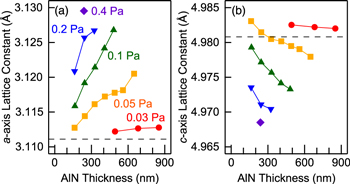
Fig. 1. (Color online) AlN film thickness dependence of the (a) a-axis and (b) c-axis lattice constants of the AlN before high-temperature annealing. The lattice constants were characterized by XRD-RSMs from the AlN (10–15) diffraction. The broken lines indicate the lattice constant of the unstrained bulk AlN.23) The values denoted as annotation in the graph are the sputtering pressure.
Download figure:
Standard image High-resolution imageThen, we conducted the high-temperature annealing of the AlN films and investigated the effects of controlling the residual stress in the films on the occurrence of cracking. Figure 2 shows the relationship between the thickness of the AlN films, the sputtering pressure, and the occurrence of cracking on the AlN films after high-temperature annealing. Excepting the samples deposited at the lowest pressure of 0.03 Pa, cracks were generated when the thickness of the AlN films exceeded certain values, regardless of the sputtering pressure. However, the threshold thickness at which cracking takes place increases with a decrease in the sputtering pressure. As already demonstrated, before annealing, AlN films with smaller thicknesses or those sputtered at a lower pressure had larger (smaller) compressive (tensile) stress. These results suggest that AlN films with larger (smaller) compressive (tensile) stress show less cracking after the high-temperature annealing. Further, the compressive stress accumulated in the as-sputtered AlN films increased their tolerance against the tensile stress applied to them during the high-temperature annealing. Thus, by lowering the sputtering pressure, relatively thick but crack-free AlN films were achieved.
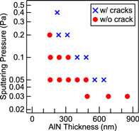
Fig. 2. (Color online) Relationship between the AlN thickness, sputtering pressure, and occurrence of cracking on the AlN template after high-temperature annealing at 1700 °C.
Download figure:
Standard image High-resolution imageFigure 3 show the dependence of X-ray rocking curve full width at half maximum (XRC-FWHM) values of the AlN films on the film thickness after annealing. Although not shown here, regardless of the thickness and sputtering pressure, the XRC-FWHM values from (0002) diffractions are lower than 12 arcsec for both before and after annealing. These values are almost the same as the smallest value limited by the resolution of the measurement system. This result indicates that the densities of screw-type or mixed-type dislocations of these samples are reasonably low. The FWHM values of the (10–12) diffractions from the samples before annealing are larger than 3000 arcsec. These values reflect the enormous twist components of the columnar domains constituting the as-sputtered AlN films. Meanwhile, in Fig. 3, the FWHM values after annealing are more than one order of magnitude smaller than those before annealing. For the samples after annealing, the FWHM values decrease as the AlN thickness increases. It can be speculated that by increasing the thickness of the AlN films, the size of AlN nuclei can be more rapidly increased during high-temperature annealing, resulting in an increased final domain size of the AlN film and reduction in the TDDs. Therefore, increasing the thickness of the AlN films without generating cracks is important for producing high-quality AlN templates.

Fig. 3. (Color online) XRC-FWHM values from AlN (10–12) diffraction after annealing as a function of AlN film thickness. Only the samples without a crack are plotted.
Download figure:
Standard image High-resolution imageFurthermore, to determine the accurate TDDs of the AlN templates, we performed STEM characterization and counted the defect structures in the plan-view STEM images with different TDDs. Prior to the STEM characterization, AlN layers were grown on these samples by MOVPE for the convenience of fabricating TEM specimens. While 0.8- to 2.8-μm-thick AlN layers were grown on the templates by MOVPE, we confirmed via XRD measurements that there is no significant difference on the twist components before and after homoepitaxy. Figures 4(a) and 4(b) show the typical cross-sectional and plan-view STEM images of the sample with a 480-nm-thick sputter-deposited AlN layer and an 800-nm-thick MOVPE-grown AlN layer. The average distance between the threading dislocations is so large that the pair annihilation of the threading dislocations during the MOVPE growth rarely occurs. Thus, although the plan-view STEM specimens were picked up from near the surface of the MOVPE-grown AlN layer and the STEM images show the features of defect that reached the surface of the MOVPE-grown AlN, the defect densities evaluated by STEM images directly reflect the TDDs of the AlN templates. Almost all the dislocation detected by STEM characterization was pure edge-type. The density of screw-type and mixed-type dislocations is lower than 3 × 106 cm−2, which can be confirmed by not only STEM but also by the AFM images [like shown in Fig. 6(b)].

Fig. 4. (a) Cross-sectional and (b) plan-view STEM images of the sample with a 480-nm-thick sputter-deposited AlN layer and an 800-nm-thick MOVPE-grown AlN layer. All the dislocations seen in these figures are pure edge-type.
Download figure:
Standard image High-resolution imageFigure 5 shows the relationship between the thickness of the AlN template and the TDDs after annealing. In Fig. 5, the AlN template thickness means the thickness of sputter-deposited and high-temperature-annealed AlN templates. As expected from the XRD measurements, TDDs decrease as the thickness of the AlN templates increases. By optimizing the annealing temperature (will be discussed elsewhere) a TDD of 2.07 × 108 cm−2 was achieved. To the best of our knowledge, this value is comparable to that of the state-of-the-art AlN films with a few-μm thickness grown on sapphire substrates.
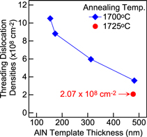
Fig. 5. (Color online) Relationship between the AlN template thickness and the TDDs estimated from the plan-view STEM images.
Download figure:
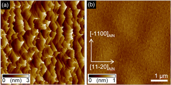
Standard image High-resolution imageLastly, we performed MOVPE homoepitaxial growth of AlN on the annealed templates and investigated the surface morphology of the AlN. Figure 6(a) shows the surface morphology of the template immediately after annealing. Bunched step structures with a height of a few atomic layers was observed. Figure 6(b) show the morphology of the MOVPE AlN film with 200 nm thickness grown on the annealed templates. Contrary to the morphology without MOVPE growth, the homoepitaxially grown AlN films exhibit step-and-terrace structures with step heights of c/2 which is similar to the morphology of AlN homoepitaxially grown on bulk AlN substrates.30) It can be seen that homoepitaxial growth of a film as thin as 200 nm is effective for solving the step-bunching, and constructing straight step-and-terrace structures arranged at equal intervals. These results prove that one can grow AlGaN-based device structures from an atomically flat surface using these sputter-deposited and high-temperature-annealed templates by inserting a thin AlN homoepitaxial layer before the MOVPE growth of the AlGaN layers.
Fig. 6. (Color online) AFM surface morphology images of (a) an AlN template immediately after high-temperature annealing with 480-nm-thick, (b) a 200-nm-thick MOVPE-grown AlN film on the template.
Download figure:
Standard image High-resolution image
In this work, the residual stress of sputter-deposited AlN films was controlled by modifying the sputtering pressure. By accumulating the compressive stress, the occurrence of cracks in the AlN films was effectively suppressed even for films with a relatively large thickness. TDD of the annealed AlN template decreased with increasing thickness of the AlN film. Finally, by optimizing the fabrication conditions, an AlN template with TDD of 2.07 × 108 cm−2 and atomically smooth surface with a thickness smaller than 1 μm was demonstrated. The reduction of the TDDs of AlN templates is likely to improve the performance of the DUV-LEDs.
Acknowledgments
The authors thank Mr. K. Norimatsu and Ms. K. Izuoka for support with sample preparation. This work was partially supported by MEXT "Program for Building Regional Innovation Ecosystem", JSPS KAKENHI Grants (JP16H06415, JP16H06418, JP17H05335, and JP17H06762), JST CREST (16815710), JST SICORP EU H2020 No. 720527 (InRel-NPower), and JST SICORP with MOST in China.