
Abstract
The recent exploration of metasurfaces reveals potential for developing virtually flat optics. In this work, a highly efficient beam splitter based on all-dielectric metasurfaces is demonstrated for visible light by finite-difference-time-domain simulations. The structure consists of a TiO2 nano-cylinder array and a layer-by-layer reflector with high efficiency separated by a SiO2 spacer. A conversion efficiency higher than 90% can be readily achieved over a wavelength range from 490 to 560 nm for the proposed device.
Export citation and abstract BibTeX RIS

Content from this work may be used under the terms of the Creative Commons Attribution 4.0 license. Any further distribution of this work must maintain attribution to the author(s) and the title of the work, journal citation and DOI.
The reflective beam splitter is a important component in optical systems. Conventional beam splitters are difficult to integrate with other optical components due to their large size and weight. Recently, metasurfaces have offered promising potential for developing virtually flat optics, thin-film optics and diffractive optics. These ultra-thin artificial planar elements, which consist of many nanoscale structural units arranged on a thin chip, can efficiently manipulate electromagnetic waves in terms of amplitude, phase, and polarization states and thus engineer their wavefronts.1–3) Their applications include super-resolution imaging,4) high precision lithography,5) and invisibility cloaks,6) as well as planar optics.7,8) Although several lightweight, ultra-thin optical elements based on metal metasurfaces have been successfully developed to facilitate the replacement of bulky optical components at microwave,9) terahertz10) and infrared11) frequencies, many problems are still unsolved. For example, due to the high insertion loss induced by the interaction between electromagnetic waves and free electrons in the metal, beam splitters based on subwavelength metal metasurfaces have extremely low efficiency in the visible spectrum.12–14) Moreover, most metal metasurfaces are designed for a single wavelength, and thus cannot achieve high efficiency in a wide band due to the wavelength sensitivity of strong resonances. To obtain highly efficient integrated optical devices, dielectric materials, which can overcome the aforementioned challenges due to their low optical loss,6,15,16) have received great interest in recent years. More importantly, they are compatible with standard semiconductor fabrication and integration techniques.17,18) Thus, dielectric-based chromatically-corrected imaging lenses,19) polarizers,20) lightweight flat lenses,21) beam shapers22) and transparent beam splitters23–25) have been developed recently.
In this letter, a high-efficiency ultra-wideband reflective beam splitter based on an all-dielectric metasurface for visible light is demonstrated using finite-difference-time-domain (FDTD) simulations. Here, the schematic of the proposed metasurface and its unit cell is shown in Fig. 1. The proposed structure consists of an array of TiO2 nano-cylinders and a layer-by-layer (LBL) high-efficiency reflector separated by a SiO2 spacer. To achieve broad bandwidth and high efficiency, amorphous TiO2 is chosen due to its relatively high refractive index and low absorption losses in the spectral range studied.19,26) The unit cell of the anisotropic coding metasurface is illustrated in Fig. 1(a), where an amorphous TiO2 nano-cylinder is designed on an LBL high-efficiency reflector separated by a SiO2 spacer. Its optical properties such as phase and polarization depend on the Mie-type resonances of each TiO2 cylinder, which can be controlled by changing the width and height of the block.

Fig. 1. (Color online) Schematic of (a) the unit cell and (b) the metasurface-based all-dielectric beam splitter.
Download figure:
Standard image High-resolution imageSix parameters are used to characterize the geometry of the unit cell structure as sketched in Fig. 1(a): P, d, h1, h2, dH, and dL. P is the period of the metasurface (P = 0.4λ0 ≈ 200 nm, where λ0 = 530 nm is the wavelength of incident light12)), and d is the diameter of the TiO2 cylinder in the top of the element. The LBL reflector is shown in the dotted square of Fig. 1(b). It consists of two alternately spliced materials with different refractive index and a thickness of a quarter wavelength at the designed frequency, which satisfies coherence conditions. Here, dH = 45 nm and dL = 91 nm are the optimized thicknesses of the high refractive index layer and the low refractive index layer, respectively, and h2 = 100 nm is the optimized thickness of the SiO2 dielectric layer. Figures 2(a) and 2(b) show the change of reflective phase and amplitude of the structure with respect to the thickness (h1) of the TiO2 cylinder height, respectively. With normally incident x-/y-polarized light at 530 nm, the reflective phase difference is higher than 180° when h1 varies from 100 to 140 nm. It can be clearly seen that the average reflective amplitude of the structure with h1 = 120 nm [pink line in Fig. 2(b)] is the highest of all those diameters. Thus, the optimized parameter for the TiO2 cylinder is h1 = 120 nm. These kinds of component can control the light wavefront using a resonator array with subwavelength dimensions, which is patterned on a surface to introduce the desired spatial distribution of optical phase. By tailoring the properties of each element of the array, one can spatially control the phase of the scattered light and consequently tailor the wavefront.
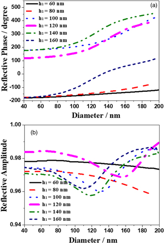
Fig. 2. (Color online) (a) Reflective phase and (b) reflective amplitude with different thicknesses of TiO2 cylinder (h1).
Download figure:
Standard image High-resolution imageFigures 3(a) and 3(b) compare the performance of the proposed device with other multilayer structures. We choose Al and SiO2 as the metal and interlayer materials, respectively. The thickness of the metal reflector is 150 nm and the period is 200 nm in both metal–interlayer–metal (M–I–M) and dielectric–interlayer–metal (D–I–M) structures. The optimized thickness of the Al cylinder layer and the SiO2 interlayer of the M–I–M nano-structure used in the simulation is 50 nm. The optimized thickness of the TiO2 cylinder layer and the SiO2 interlayer of the D–I–M nano-structure is the same as that of the all-dielectric one. It is noticed that high reflective phase difference can be obtained in both types of nano-cylinder, as shown by the black and green dotted lines in Fig. 3(a). However, the average reflective amplitude of the M–I–M and the D–I–M nano-structures (black and green dotted lines, respectively) is much lower than that of the all-dielectric one (red line) due to ohmic losses in the metal and the influence of Fabry–Pérot (F–P) interference phenomena within the multilayer structure,27,28) as illustrated in Fig. 3(b). Since the light wavefront can be controlled efficiently in the proposed all-dielectric element using arrays of optical resonators with subwavelength dimensions, the phase of the scattered light and the wavefront can be spatially controlled.
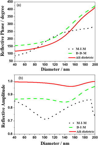
Fig. 3. (Color online) Comparison of the performance of the proposed all-dielectric multilayer with that of other multilayer structures.
Download figure:
Standard image High-resolution imageApart from their high efficiency, wide bandwidth is also preferred in the all-dielectric structure. As shown in Fig. 4(a), when the diameters of the TiO2 nano-cylinders are 66 nm and 196 nm, respectively, the phase difference of the reflected light is close to 180° from 490 to 560 nm. By periodically arranging "66 nm" or "196 nm" unit cells in alternating columns along the x-axis/y-axis, abrupt phase variations in the x-axis/y-axis directions are achieved. Therefore, the TiO2 nano-cylinder array with the same structural parameters has the ability to split light with different wavelengths. Figure 4(b) shows that the reflection amplitudes are above 0.95 in the wavelength range 490–560 nm. This may arise from two aspects: one is that the LBL high-efficiency reflector has ultra-wide working range, which can fully reflect the broadband light, and the other is that the top TiO2 cylinder has ultra-low loss in ultra-wide bandwidth.
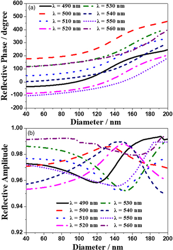
Fig. 4. (Color online) (a) Reflective phase and (b) reflective amplitude with incident light of different wavelengths.
Download figure:
Standard image High-resolution imageHere, we give an example with x-polarization. As shown in Fig. 1(b), a high-efficiency and ultra-wideband beam splitter based on an all-dielectric reflector array metasurface is demonstrated using FDTD simulations. Assuming perfectly matched layers in the z-axis direction, we set the periodic boundary conditions in the x- and y-directions. The distribution of cells follows the rules that two columns of "66 nm" unit cells and two columns of "196 nm" unit cells are distributed alternately along the x-axis. The incident x-polarized light is designed to project onto the metasurface along the z-axis and the deviation angle of reflected light with respect to the z-axis is exactly equal to the anomalous reflected angle determined by the generalized Snell's law2)

where λ0, p and Γ represent the free-space wavelength, the period of the unit cell, and the period of the dielectric metasurface sequence, respectively. By changing the size of the dielectric metasurface sequence, the required reflection angle can be achieved according to the relationship between λ0 and Γ. When the incident light projects onto a metasurface vertically, substituting λ0 = 530 nm, Γ = 800 nm (n = 4, p = 200 nm), and θi = 0° into Eq. (1), the deviation angle θr with respect to the z-axis can be calculated to be about 41.2°. Since the phase gradients in the positive and negative x-axis directions are nearly the same as each other, the reflection is directed at two deviation angles of ±41.2° with respect to the z-axis.
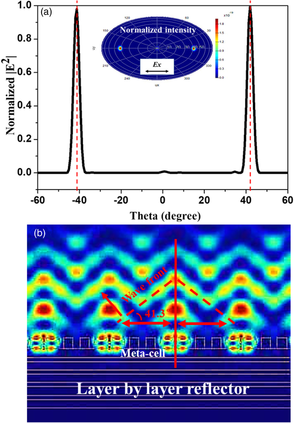
The normalized far-field radiation and scattered electric field patterns of x-polarization under the illumination of normally incident x-polarized light at 530 nm are given in Figs. 5(a) and 5(b), respectively. It can be seen from the inset polar diagram of Fig. 5(a) that two well-defined light beams are clearly formed. The x–z cut of all reflected beams (black line) depicts that the mirror reflection is very low and the anomalous reflection is very high, which indicates that a very high conversion efficiency can be achieved. It can be seen from Fig. 5(b) that almost all the energy can be abnormally reflected from the all-dielectric metasurface, and the phase profile can be validly obtained with the all-dielectric metasurface. The dashed line defining the wavefront shows that the simulated reflection angles are both 41.3°, which shows good agreement with the calculated value (41.2°).

Fig. 5. (Color online) (a) FDTD-simulated normalized far-field radiation pattern of the reflected beam for x-polarized illumination with λ = 530 nm and the inset polar diagram of normalized intensity, showing the beam is reflected at two deviation angles of ±41.3° with respect to the z-axis. (b) FDTD-simulated scattered Ex field patterns of the all-dielectric metasurface under the illumination of normally incident x-polarized light with λ = 530 nm. Phase profile obtained by the metasurface with the dashed line defining the wavefront.
Download figure:
Standard image High-resolution imageMeanwhile, the bandwidth of the device is also studied. The reflection of the whole system under x-polarized illumination across the whole visible spectrum is shown in Fig. 6(a). The reflection efficiency of the all-dielectric metasurface (red line) is higher than 95% over a wavelength range from 490 to 570 nm (red line), and it should be noted that the reflection efficiency of the whole system is about 96.3%, which is about 1.2 times that of the traditional Al–SiO2–Al structures with optimized parameters (black line) and more efficient than the D–I–M one (green line).

Fig. 6. (Color online) (a) FDTD-simulated reflection of the whole system under the illumination of normally incident x-polarized light through the whole visible spectrum. (b) Normalized FDTD-simulated scattered field intensity.
Download figure:
Standard image High-resolution image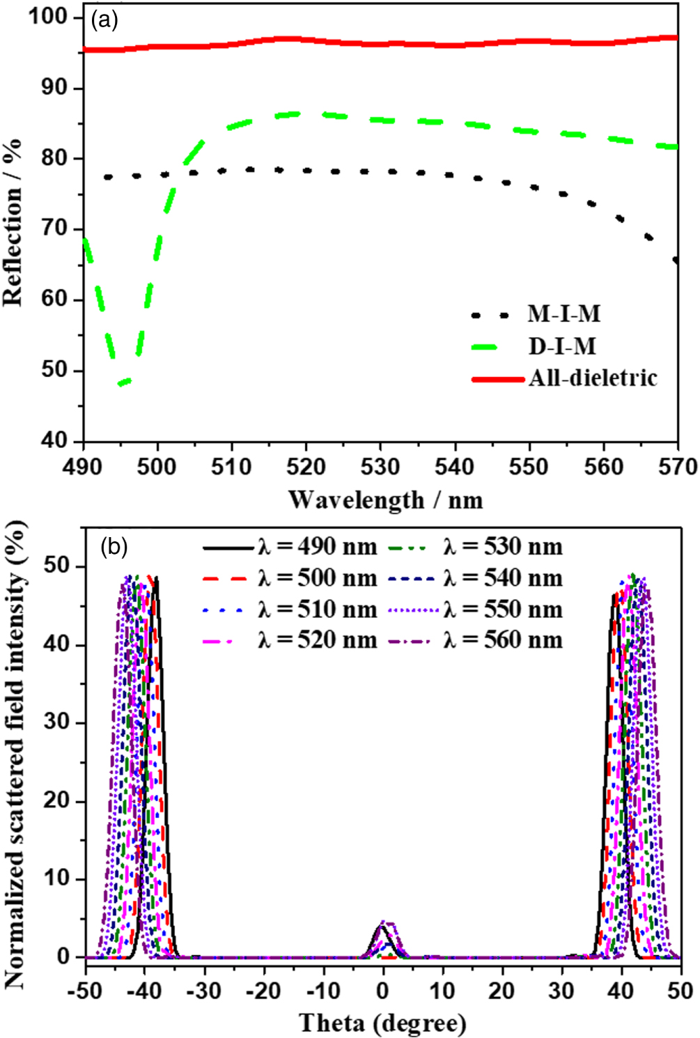
For the metasurface with fixed structure illuminated by normally incident x-polarized light with different wavelengths, the normalized scattered field intensity [P (θrn, λ)/P0]29) as a function of reflected angle θrn is shown in Fig. 6(b), where n = ±1 represents ±1 order anomalous reflected light, and P (θrn, λ) and P0 are the scattered field intensities of anomalous reflected light and incident light, respectively. The curve line exhibits two kinds of peak; one is the specularly reflected beam leaving the metasurface perpendicularly and the other is the anomalous reflection mode distributed at different locations on either side of the x-axis, symmetrically. Clearly, the proposed all-dielectric device has good characteristics over a wide spectrum from 490 to 560 nm. Specular reflection is very weak and most of the energy is efficiently reflected abnormally.
The definition of conversion efficiency for this device is η = [P (θr+1, λ) + P (θr−1, λ)]/P0. According to the data in Figs. 6(a) and 6(b), conversion efficiencies30,31) of 90.71%, 92.7%, 92.52%, 93.21%, 94.74%, 92.49%, 91.8% and 90.28% are obtained for 490, 500, 510, 520, 530, 540, 550 and 560 nm, respectively. This indicates that the device we designed here has good performance at multiple wavelengths and is acceptable for practical applications.
In summary, we have proposed a high-efficiency, broadband reflective beam splitter based on an all-dielectric metasurface for visible light. It consists of a TiO2-based nano-cylinder array and an LBL reflector separated by a SiO2 spacer. The proposed beam splitter exhibits excellent abnormal reflection capability, and a conversion efficiency of higher than 90% over a 70 nm bandwidth (490–560 nm) can be readily demonstrated. Such a minimized planar structure may lead to many practical applications in compact photonic integrated circuits in the future.
Acknowledgments
C. J. gratefully acknowledges the NANO-X workstation and interdisciplinary innovation team of the Chinese Academy of Sciences, Jiangsu Province, Suzhou City, Suzhou Industrial Park. Y. L. acknowledges Dr. Yifei Zhang at the Center of Nanoelectronics and School of Microelectronics, Shandong University, Shandong Province, Jinan City.
Funding
Jiangsu Key R & D Programs (BE2018006-3), National Natural Science Foundation of China (No.61674163) and the Executive Programme of Scientific and Technological Cooperation between Italy and China (2016YFE0104100).