


Abstract
The total solar irradiance at the top of the atmosphere is the primary source of energy of the Earth's highly coupled atmosphere–land–ocean system. Small fluctuations of the solar flux density in scales from years to millennia could impact the energy balance of this system due to nonlinear effects. The quantification of this variability depends on absolute radiometers on board of space-based platforms. Although there has been significant improvement in the design and calibration of absolute radiometers during the last decades, the uncertainties in the measurements have not allowed us to untangle the natural and anthropogenic drivers of the observed changes of the climatic patterns appropriately. One of the critical components of the absolute radiometers is the coating of the sensor elements, which should absorb the radiation efficiently. Here we discuss the optical characteristics of ultra-black Nickel–Phosphorus (Ni–P) and its relations with the surface morphology. The ultra-black Ni–P has important unique properties such as low reflectance and uniformity of deposition in complex geometries. Ni–P multilayer was deposited by electroless on aluminum substrates. The surface was etched by oxidizing acid to produce ultra-black Ni–P. Characterization techniques were used to describe the properties of the material. We describe the directional reflectance employing the bidirectional reflectance distribution function. Additionally, we used reflectance maps to show the influence of the pores on the reflectance. Ultra-black Ni–P exhibited a high absorptance and dependence with the light incidence angle. Based on the results, the material demonstrated the opportunity of many terrestrial and space applications as a black coating absorber.
Export citation and abstract BibTeX RIS
1. Introduction
Absorbing materials for solar radiation have an intense attraction in different fields of science and technology. Black coatings are used extensively in the naval and aerospace industry (Folgueras et al. 2010; Walter et al. 2017), in photothermal conversion (Wang et al. 2008), and especially in optical instruments such as telescopes to minimize the effect of stray light (Vieira et al. 2014). Some materials are recognized for ultra-black outstanding optical performance and high solar absorptance (α; Johnson 1980). The diverse applications of black materials with specific optical characteristics require the development of new processes. Thus, the characterization of the surface reflective properties is essential to improve the required coating optical performance. The Nickel–Phosphorus (Ni–P) alloy is a widely accepted protective coating due to its high corrosion resistance and excellent wear resistance properties. Electroless Ni–P alloys are classified as low, medium, or high according to their P content (ASTM B733-15). The P content affects alloy structural, chemical, electrochemical, and mechanical coating properties (Daly & Barry 2003; Cui et al. 2006; Pillai et al. 2012). Ni–P alloys with the appropriate P content and attacked by an oxidizing acid produce exceptionally high light absorption capability. In 1980 Johnson patented this method, producing an ultra-black surface coating associated with a unique surface morphology consisting of a dense array of pores (Johnson 1980). This coating was first applied in the space environment at an active cavity radiometer for measuring total solar irradiance (TSI) by the Total Irradiance Monitor instrument on board the Solar Radiation and Climate Experiment (SORCE) spacecraft. The ultra-black Ni–P being metal has advantages over traditionally black paints, providing robustness on-orbit (Kopp & Lawrence 2005; Kopp 2014) by exposure to the ultraviolet (UV) radiation and outgassing due to high vacuum level and atomic oxygen (AO) in low Earth. Black paints, such as MAP-PU3 used in satellites (Vasconcelos et al. 2006) and instruments (Fürmetz 2012; Walter et al. 2017), usually have a polymeric matrix and use carbon as a pigment. Black paints revealed a significant decrease in solar absorptance due to damage to organic chemical bonds or atomic oxygen erosion of the paint. Also, ultra-black Ni–P being a metal absorbs solar energy and conducts heat to the thermal link quickly.
Our research consists of multilayer Ni–P deposition on an aluminum substrate using electroless and blackening processes. This paper presents an investigation of the Ni–P surface and optical properties. The ultra-black Ni–P coating optical characteristics allows for its use in the optical systems instruments such as the telescope (Vieira et al. 2014) and as the absorptive cavity's interior for absolute radiometer to convert radiant energy into heat by the process of absorption (Berni et al. 2017).
In Section 2, we describe the Ni–P deposition procedure and the optical characterization setups, while in Section 3, we present the results:
- (1)the coating structure;
- (2)the analysis of the coating composition and morphology;
- (3)the reflectance maps, which describe the material homogeneity and identify high reflectivity spots;
- (4)the bidirectional reflectance distribution function (BRDF) that provides the porous surface influence on scattering uniformity; and
- (5)the development of an active cavity model.
2. Experimental Procedure
2.1. Ni–P Deposition and Blacking Process
The high solar absorber was obtained by the etching process of Ni–P electroless plating. The Ni–P deposition process is described as follows. The aluminum alloy (Al-98.2 Wt%, Si-1.2 Wt%, and Mg-0.6 Wt%) substrates with a 30 mm diameter were mechanically polished with SiC paper. Each sample was degreased in an acetone ultrasonic bath, Ridoline® solution (alkaline degreasing, Henkel products), and was subsequently activated by etching in 15 vol% nitric acid (HNO3) and 6 vol% sulfuric acid (H2SO4), at 70°C. A double zincate treatment was done using Alumon EN® (zincating solution).
The Ni–P electroless bath included nickel sulfate (NiSO4.7H2O, 30 g L−1) as nickel source, sodium hypophosphite (NaH2PO2, 10 g L−1) as a reducing agent, sodium citrate (Na3C6H5O7 · 2H2O, 12 g L−1), sodium acetate (CH3COONa, 5 g L−1), and thiourea (NH2CSNH2, 1 mg L−1). The bath pH was maintained in three different steps: 4.90 ± 0.05 for 160 minutes, 4.30 ± 0.05 for 100 minutes, and 4.00 ± 0.05 for 180 minutes. The three steps were used to obtain multilayers of Ni–P with different phosphorus content using the same bath. The pH was adjusted using a sulfuric acid and ammonia solution. After the deposition, the surface was etched with an oxidizing acid (HNO3, 9M) at 40°C during 40–60 s to produce ultra-black Ni–P.
2.2. Materials Characterization
The morphology images were taken using the scanning electron microscopy–field emission gun (SEM–FEG) by TESCAN MIRA 3 equipped with an energy dispersive X-ray spectroscopy (EDS) for an elemental analysis. The surface roughness of the samples was characterized using a surface profilometer, Wyko NT1100. The coatings were characterized by X-ray diffraction (XRD; Panalytical X'Pert PRO) to investigate the crystal structure and Scherrer's equation (Langford & Wilson 1978) was used to estimate the average of the particle size:

where λ is the wavelength of the X-rays; β is the full-width at half maximum of the X-ray peak; k is the shape factor, dimensionless, usually taken close to unity; and θ is the diffraction angle.
2.3. Optical Properties
The BRDF device was developed at the National Institute for Space Research and a comprehensive description and system characterization are given by Berni et al. (2015). The system is composed of a rotating arm to collect the light in the zenith direction from −70 to +70 degrees and in the azimuth angle over 360 degrees (Figure 1(A)). The halogen light source (50 W) is mounted on a turntable arm that can rotate from 0 to 60° in the zenith direction. The scattered collected light wavelength can be selected by a set of interference filters with an average bandwidth of 8.0 nm. The detector used is a Si photodiode (Oriel 70336). The BRDF measurement was calculated according to Bartell et al. (1981). The measurements were made in pairs, a sample and a reference with Lambertian reflectance National Institute of Standards and Technology (NIST)-traceable Spectralon® (Labsphere Inc., SRS-99). They were quantified by their voltages, Vref and Vs, in the following way:

where θi is the incident zenith angle, θr is the reflected zenith angle, φi and φr are the incident and reflected azimuth angles. The method requires reference data for each measured position (ρref).
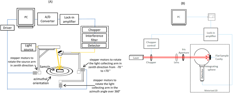
Figure 1. Schematic drawing of the BRDF measurement system (A) and the reflectance maps facility (B). Red and yellow lines represent the path of the light and the blue line represents the commands.
Download figure:
Standard image High-resolution imageThe spatial reflectance device mapped the sample over an area of ∼50 mm2 using the experimental setup shown in Figure 1(B). Three laser wavelengths at 375, at 532, and at 633 nm were used as the light source. The light goes through a collecting lens and focuses on the center of the entrance and exit of the integrating sphere. The integrating sphere was mounted on a platform to move on two axes. The reflected light was measured using a Si photodiode detector. More details of the experimental setup can be found in Suter (2014).
The results (Vs) for each position were measured relative to an NIST-traceable standard (Labsphere Inc., SRS-02) as reference (Vref):

where the dark current signal (Vdark) was acquired to provide the system with stray light and then it is subtracted from the Vs and Vref.
3. Results and Discussion
3.1. Coating Structure
Ultra-black Ni–P coatings (Figure 2) were obtained by etching Ni–P as deposited. Figure 3 presents the XRD of Ni–P as deposited and after etching. The x-ray diffractogram shows two broad coalescing peaks around 44° and 52°. It corresponds to the pattern reference reflections of Ni (111) and Ni (200) planes. As phosphorus concentration increases, the peaks become broad, indicating the continuous Ni grain size decrease (Mahalingam et al. 2007; Pillai et al. 2012). The codeposition of phosphorus in octahedral interstitial on the Ni faced centered cubic (FCC) lattice leads to expansion and structure distortion (Daly & Barry 2003). Alloys with lower P content are a crystalline and microcrystalline solid solution of phosphorus in nickel. As the P content increases, the deposit structure undergoes transition from crystalline to nanocrystalline and becomes amorphous above 9 wt% of P (Agarwala & Agarwala 2003; Pillai et al. 2012). The Scherrer analysis indicates the structure crystallite size to be 1.66 nm and 2.48 nm for Ni–P and ultra-black Ni–P, respectively. For crystallites with sizes less than about 200 nm, the distinction between alloys being finely crystalline and amorphous could be inaccurate (Brown et al. 2002).
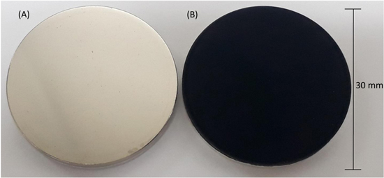
Figure 2. Ni–P coating before (A) and after etching (B).
Download figure:
Standard image High-resolution image
Figure 3. XRD patterns of the Ni–P as deposited and ultra-black Ni–P.
Download figure:
Standard image High-resolution image3.2. Coating Composition and Morphology
It is well known the Ni–P alloy phosphorus content and morphological structure influence the chemical (Riedel 1991), electrochemical (Gu et al. 2005; Elias et al. 2016), and mechanical properties. The electroless deposits content are strongly dependent on the bath composition, pH, temperature, and loading factor (the ratio between the substrate area and solution volume). Different electroless Ni–P coating characteristics can be obtained by adjusting the plating bath variables. The concentration of nickel metal and the phosphorus source can affect the bath equilibrium and the optimum quantity ratio can improve the efficiency of deposition (Osifuye et al. 2014; Sun et al. 2015).
Electroless deposition processes are a heterogeneous reaction. The electrochemical mechanism (Malecki & Micek-Ilnicka 2000) establishes that for each mole of metal deposition, three moles of H+ are produced during the reaction progress. Several authors have demonstrated the effect of pH in the Ni–P composition (Sudagar et al. 2013; Sun et al. 2015). The decreasing of pH results in nickel deposits with higher P content and a lower deposition rate. The main reason is due to pH's influence on the Ni and P speed reaction. Generally, when the pH of the bath reduces, there is a higher rate of P formation and lower Ni formation (Anijdan et al. 2018). Ni–P presented a typical cauliflower morphology (Figure 4) consisting of globular grains due the tendency of Ni–P precipitates (with higher phosphorus contents) for spheroidization to reduce surface energy. The spherical shape and size depends on the deposition rate and the nucleation sites on the surface (Anijdan et al. 2018).
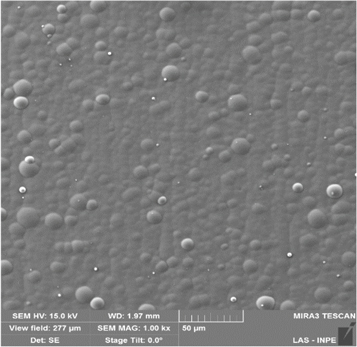
Figure 4. SEM micrograph of Ni–P surface as deposited.
Download figure:
Standard image High-resolution imageFigure 5 shows SEM images of the cross-sections of Ni–P (A) and ultra-black Ni–P (B). An EDS cross sectional elemental line scan consists of the analysis of the major alloying elements of the coating (Ni and P) and substrate (Al) across the layer. According to Figure 5(C), the phosphorus content progressively decreased due to the pH maintained during electroless deposition. The P content varies from 10.3 wt.% P at the top to 4.8 wt.% P near to the Ni–P/Al interface, indicating the multilayer coating formation. The P content along the layer can be classified as medium (5 to 9 wt.% P) and high (more than 10 wt.% P) according to ASTM B733-15.4 The phosphorus content has a substantial influence on Ni–P alloy properties. The low P (1 to 2% P) is rapidly attacked by acid, and the higher P content was more resistant to acid attack than pure metal (Brenner et al. 1950). When Ni–P coating is etched by oxidizing acid, the coating turns black. Brown et al. (2002) had found the influence of phosphorus content before etching in the morphologies and optical properties of black nickel surfaces. They also observed the ultra-black Ni–P coating's lowest reflectance with P content is between 5 and 9%. In preliminary results, we tested the influence of phosphorus content through different pH maintenance approaches. Initially, the pH was adjusted only at the beginning of operation or it was kept constant during the deposition time. However, our experimental results show the lowest reflectance and deeper black surface etching with a multilayer coating. The blue dotted line (Figure 5) corresponds to the approximate thickness of the Ni–P film removed in the acid etching. The region with a continuous decrease in P (∼13 μm) was removed in the acid etching. In this configuration, the phosphorus content is higher at the top and decreases along the layer. We propose that the outermost layer is attacked for a long time due to the higher P content, and as the oxidizing solution penetrates the lower P content, it is more easily attacked, forming deeper pores. Surfaces with higher phosphorus contents at the top were not attacked with the method employed.

Figure 5. SEM micrograph cross section for the Ni–P as deposited (A) and ultra-black Ni–P (B). This shows EDS line-scan analysis for the trend in the concentration of major elements Ni (green) and P (red) in the coating and Al (pink) in substrate for Ni–P as deposited (C) and after acid etching (D). The dotted line is the approximate region etched by the acid.
Download figure:
Standard image High-resolution imageThe pores have a crucial role in obtaining low reflectance (Johnson 1980; Brown et al. 2002; Saxena et al. 2006). They confine the radiation leading to multiple internal reflections until the absorption. This unique morphology (Figure 6) is a result of the etching process. It is strongly influenced by the Ni–P for deposited coating properties and the blackening process conditions. The oxidant acid attacks the nickel atoms preferentially (Cui et al. 2006) and it is responsible for oxide film (NiO and NiO2) formation (Stupnišek-Lisac & Karšulin 1984). The different pore diameters and depths can be attributed to the coating composition variability and structure defects. The pore depths reach up to 25 μm and have different shapes. Figure 7 shows ultra-black Ni–P roughness profiles in the sample center and near the edge (∼0.6 mm from the edge). The roughness parameters (Ra) were computed by averaging the distance from the measured point to the mean plane. The Ra values obtained were 1.7 to 4.2 μm. The average roughness parameter confirms the non-uniformity along the surface. This variation can be attributed to the variability of acid etching along the surface. The scattering properties are directly related to surface roughness and wavelength. There is a relationship between the diffuseness or glossiness and the parameter Ra. As Ra gets smaller, there is a tendency to increase the glossiness (Yonehara et al. 2004).
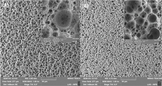
Figure 6. SEM micrograph of ultra-black Ni–P surface etching by 60 s (A) and 40 s (B).
Download figure:
Standard image High-resolution image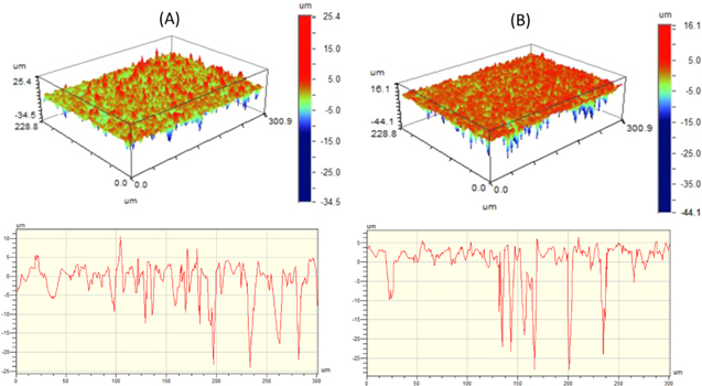
Figure 7. Three-dimensional (3D) optical profilometry surface and the 2D profile of ultra-black Ni–P in the central position of the sample (A) and near the edge (B).
Download figure:
Standard image High-resolution image3.3. Reflectance Maps
To investigate the black Ni–P absorption (α) features, the reflectance (1−α) was measured. An 8 mm diameter circle in a flat sample was scanned line by line with a line/point step of 0.3 mm. The laser was focused on multiple locations normal to the surface, and the reflected light was measured. Figure 8 shows the 2D (X–Z) reflectance maps and the reflectance average results are listed in Table 1. The absorptance average over the illuminated area is 99.71%, 99.77%, and 99.81% at 375 nm, 532 nm, and 633 nm, respectively. The results show a wavelength-dependent absorptivity influence of about 0.1%. The reflectance is distributed in the same sample within the range of 1554–6288 ppm at 633 nm. The reflectance maps provided an understanding of the impact of the size and depth of the pores formed in the etching process (see also Section 3.2). The maps showed that the reflectance is non-uniform over the surface and demonstrated the existence of different intensity with some points of higher reflection. The non-uniformity suggests that the etching process removes more intense material in regions rich in nickel. Consequently, regions rich in nickel present a different morphology and thickness of the black layer than the overall surface, which determines the electromagnetic radiation absorption characteristics (Brown et al. 2002). As expected, the reflectance varies in different sample regions due to the inherent electroless characteristics variability and the blackening process.
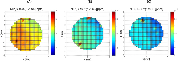
Figure 8. Ultra-black Ni–P reflectance maps measured at 375 nm (A), 532 nm (B), and 633 nm (C).
Download figure:
Standard image High-resolution imageTable 1. Ultra-black Ni–P Map Average Reflectance
| Wavelength | Average Reflectance | Standard Deviation |
|---|---|---|
| (nm) | (ppm) | (ppm) |
| 375 | 2926 | 86 |
| 532 | 2275 | 112 |
| 633 | 1928 | 57 |
Download table as: ASCIITypeset image
3.4. BRDF
Figure 9 shows the reflectance profile measured in three incident zenith angles (15°, 30°, and 60°) at 500 nm. The distributions are bell-shaped, which resulted from diffuse reflectance. The profiles show the distribution variation in a function of incident zenith angles. Although predominating diffuse reflectance for θI = 15° and θI = 30°, a component that coincides with specular reflection (Figure 10) is observed. Larger zenith angles cause an increase in the BRDF. Figure 11 shows the reflectance obtained by total integrated scattering (TIS). The increment in the incident zenith angles increases the reflectance. Ultra-black Ni–P has low wavelength dependence on the reflectance at θI = 15° and θI = 30° between 500 and 800 nm. However, there is a reflectance increase in the function of wavelength at θI = 60°.

Figure 9. BRDF profile and top view reflectance points measured for the ultra-black Ni–P with incident zenith angles at 15° (A), 30° (B), and 60° (C) in Cartesian coordinates where X represent the azimuth (φR) and Y represents the zenith angle (θR).
Download figure:
Standard image High-resolution image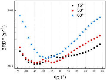
Figure 10. BRDF for three different incident zenith angles at φR = 0°.
Download figure:
Standard image High-resolution image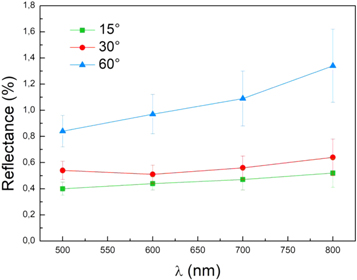
Figure 11. Total reflectance as a function of the wavelength for the ultra-black Ni–P surface at three different incident angles.
Download figure:
Standard image High-resolution imageThe ultra-black Ni–P surface morphology has a significant influence on the reflectance. The incident beam at lower angles results in low reflectance due to the ability of the electromagnetic radiation to enter and interact with the pores. These interactions repeatedly occur until the electromagnetic radiation is almost completely absorbed. The pores perpendicular to the surface confine the incident light (Amemiya et al. 2012; Kodama et al. 1990). In this way, the highest incident angles may have part colliding with the lateral wall of the pores, resulting in a reflectance increase. The ultra-black Ni–P optical properties with a thicker absorption layer yield a lower spectral reflectance, especially at longer wavelengths. Ultra-black Ni–P with low reflectance depends on several parameters such as pore depth and size, the thickness of the absorption layer, and the geometric factor of incident light and porous position.
3.5. Effect of Reflectance Geometric Parameters on TSI Sensors
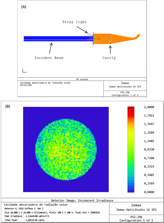
The BRDF analysis indicated the scattered light depends on the incidence angle, with the absorptance of the Ni–P film decreasing from 99.77% at θI = 0° to 98.4% at θI = 60°. Although it is high absorption, it is desirable to design absolute radiometers with even a higher absorption. We can increase the overall absorptance by employing cavities instead of flat surfaces. Most of the absolute radiometers designed for TSI measurements are based on this approach to improve the absorption of solar radiation. To estimate the absorbtance of cavities, we model a cone-shaped cavity by employing an optical engineering software (Zemax® OpticStudio). Figure 12(A) shows the model configuration. An 8 mm diameter beam in front of the instrument illuminates the cavity, which has a diameter of 17 mm and a length of 71 mm and its internal coating is based on the experimental BRDF data. We used the mode non-sequential (NSC) ray-tracing, where which rays hit the objects depends upon the object geometry and the angle and position of the input ray (ZEMAX 2016).
Figure 12. NSC 3D layout of the reflection cavity in Zemax® (A). A detector in the non-sequential mode is used to visualize light coming out of the cavity (B).
Download figure:
Standard image High-resolution image
Figure 12(B) presents the results of the irradiance distribution of the reflected beam in a virtual detector rectangle (size: 20 × 20 mm and pixels: 100 × 100) positioned in front of the cavity. The color code indicates the flux density (W m−2) in the pixel area. It is noticeable that the reflected flux out of the cavity is non-uniform, with a higher flux density at the center region of the cavity. This pattern occurs due to the result of the geometric relationship among the incident beam, cavity geometry, and the pores perpendicular to the cavity surface. The salt-and-pepper flux distribution seems to be due to the incident angle of the beam in the pores.
The estimated absorption for the modeled cavity is approximately 99.9998%. However, we expect lower absorption in real cavities due to the inhomogeneous distribution of the coating Ni–P that arises during the deposition process.
4. Concluding Remarks
Absorber materials play a crucial role in optical instrument design, as they can be employed to minimize stray light in instruments such as spectrograms, polarimeters, microscopes, and telescopes. On the other hand, these absorber materials are the main critical elements of devices, such as active cavity absolute radiometers, as their design requires that the sensor element absorbs most of the incoming radiation. Here, we reported a method to produce an ultra-black Ni–P film based on the electroless deposit of multilayer Ni–P film and acid etching.
Based on the X-ray analysis, which allowed us to identify the nanocrystalline—amorphous structure of the Ni–P film, we concluded that the black coating conversion process is influenced by Ni–P (as deposited) properties and the chemical attack variables.
To study the influence of the morphology on the reflectance properties, we analyzed the SEM–FEG images and reflectance maps. The SEM–FEG image analysis revealed the morphology of a large number of pores of various shapes and sizes, while reflectance maps showed that pore irregularity results in non-uniform surface reflectance. This study suggests that the morphology of the Ni–P film influences its reflectance properties. While the absorptance of ultra-black Ni–P is estimated to be above 99.7% on the analyzed wavelengths, the scattered light depends on the incidence angle. The BRDF analysis indicated that absorptance of the Ni–P film decreases from 99.77% at (θI = 0°) to 98.4% at (θI = 60°). The dependence on the incident angle seems to be because perpendicular pores to the surface act as traps for the incident light. Moreover, the BRDF analysis showed that the shape of the curves varies with the viewing angle. In general, we observed that as the incidence angle increases, the TIS increases.
For the selection of the absorber material for optical instruments, it is necessary to have a thorough understanding of optical properties resulting from its porosity and roughness. There are a variety of materials and processes that can be employed for the blacking of surfaces, including anodization, paint, and carbon nanotubes. For the selection of the absorber coating material, it is necessary to take into account several properties, such as the optical, mechanical, and thermal properties, as well as the environmental requirements. Carbon nanotubes have been investigated as viable candidates for many optical applications for the blacking of surfaces, especially by employing the chemical vapor deposition process (Lehman et al. 2018). However, at this point, electroless Ni–P deposition is more straightforward and does not require substrates with high melting points. On the other hand, the electroless plating process requires a catalytic surface or activation is required.
We concluded that ultra-black Ni–P is an excellent absorber for application on the detection and measurement of the radiation as an absolute radiometer and thermocouple. Our study highlighted that the BRDF analysis is required to model the reflective properties and performance of optical instruments. Moreover, the choice or development of the absorbing surface coatings should be tailored for each specific application's requirements.
We thank the anonymous referee for valuable comments and suggestions that helped improving this paper. This work is partially supported by CNPq/Brazil and CAPES/Brazil. Special thanks to Physikalisch-Meteorologische Observatorium Davos/World Radiation Center/Switzerland (PMOD/WRC) for hosting F.C. and supporting the reflectance maps measurements. Thanks to the Plasma Physics Group at USP for OpticStudio.