

Abstract
GaN monolithic microwave integrated circuits (MMICs) on a diamond heat spreader were successfully fabricated and demonstrated. The diamond was bonded to the back-side surface of the GaN on SiC devices by atomic diffusion bonding. In addition, through-substrate vias (TSVs) of diamond and SiC were fabricated using a deep dry etching process. This study marks the first development of GaN MMIC on diamond with TSVs fabricated using diamond etching. From the large-signal measurement of GaN MMICs at 7 GHz, the output power of the device with diamond during continuous wave operation was improved by 11% compared to that of without diamond.
Export citation and abstract BibTeX RIS
GaN-based high electron mobility transistors (HEMTs) are suitable for microwave and millimeter-wave amplifiers with their high-output-power and efficiencies in long-distance radio-wave applications, such as weather radars and wireless network systems. 1–8) To expand the range of radio-waves with small chip sizes, high-output-power GaN HEMT amplifiers are crucial. However, self-heating effects under high power operations increase the channel temperature resulting in the degradation of device performance. 9,10) Therefore, effective thermal management of devices is a key technology for high-power operations. Diamond is a promising material for integrated heat spreaders for GaN HEMTs because of its high thermal conductivity. 11–19) We have previously reported that S-band GaN HEMTs on diamond heat spreaders were successfully fabricated using a room temperature bonding technique, which resulted in increased output power owing to the high heat dissipation of diamond heat spreaders. 20,21)
GaN monolithic microwave integrated circuits (MMICs) integrate GaN HEMTs and passive devices, such as metal–insulator–metal capacitors and thin-film resistors. Through-substrate vias (TSVs) are generally used for ground connections. 22–28) Because the ground used in the circuits can be electrically connected to the back-side at a short distance, the circuits operate stably. To realize GaN MMICs on diamond heat spreaders (GaN/diamond MMICs), shown in Fig. 1, a TSV fabrication technique through diamond is required. Most TSVs in GaN MMICs are fabricated using laser drilling 22–24) or dry etching processes. 25–28) Lee et al. reported that the fabrication of TSVs with diamond through laser drilling was applied to GaN HEMTs. 29) However, the electrodes may be melted due to laser processing, which causes disconnections. In addition, the residue generated by the laser ablation may cause a short between the electrodes. Therefore, it is difficult to use laser drilling for the fabrication of GaN MMICs because all TSVs are required to ensure conduction between the electrodes on the front- and back-side surfaces. Moreover, there are also problems related to difficulties in controlling alignment and the opening size in TSVs fabrication through a laser drilling process. In contrast, with dry etching, the alignment and size of TSVs can be easily controlled using an etching mask formation. Moreover, dry etching has the advantage that it can be processed at low temperature without damage. However, to etch diamond, it is necessary to select an appropriate etching mask, and there are only a few reports on diamond deep etching. As far as we know, there are no reports on the fabrication of GaN/diamond MMICs with TSVs using a dry etching process. In this study, we have developed a novel technique for fabricating diamond TSVs using a deep dry etching process. In addition, we have successfully fabricated GaN/diamond MMICs with TSVs. We also confirmed the effect of the diamond heat spreader by measuring the output power with CW operation at 7 GHz.
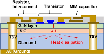
Fig. 1. (Color online) Schematic of the cross-section of our GaN/diamond MMIC.
Download figure:
Standard image High-resolution imageA process flow for a back-side process of GaN/diamond MMICs is shown in Fig. 2. Following the device fabrication on the front-side [Fig. 2(a)], the SiC substrate on the back-side of the device was thinned to 25 μm, and the back-side surface was smoothened by chemical mechanical polishing (CMP) prior to diamond bonding [Fig. 2(c)]. Then, the diamond was bonded to the back-side surface of SiC using atomic diffusion bonding (ADB) [Fig. 2(d)]. 30) (100) single-crystal diamond (thermal conductivity of ∼ 2000 W m−1 K−1) fabricated by chemical vapor deposition (CVD) were used as heat spreaders. ADB is a room temperature bonding through the self-diffusion of metals. 30) It is a promising bonding method for achieving a low interfacial thermal resistance of SiC/diamond because it does not require thick adhesive layers. To bond with ADB, it is necessary to make both the bonding surfaces of the SiC and the diamond extremely smooth. Based on previous studies, we successfully smoothened diamonds using both mechanical polishing and CMP with a surface roughness (Ra) of less than 0.5 nm. 17) After diamond bonding, the diamond was thinned to 80 μm by dry etching without etching masks [Fig. 2(e)]. In this study, the width and length of transmission lines of the matching circuit of the MMICs was designed with a SiC thickness of 100 μm. Therefore, thicknesses of SiC and diamond were chosen so that the effective dielectric constant of the substrate would be close to that of the conventional 100 μm SiC. Then, an etching mask for TSV etching was patterned with photolithography and electrodeposition processes [Fig. 2(f)]. Subsequently, diamond-TSVs etching [Fig. 2(g)] and SiC-TSVs etching [Fig. 2(h)] were carried out using the same etching mask. Au TSVs interconnects were fabricated through electrodeposition [Fig. 2(i)]. Finally, the temporally supporting wafer was removed [Fig. 2(j)].
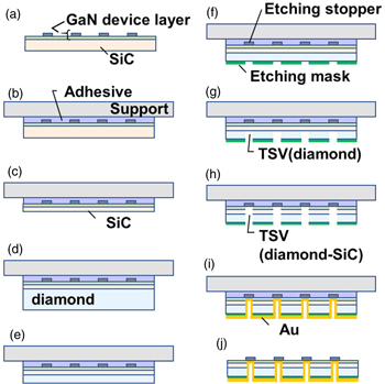
Fig. 2. (Color online) Back-side process flow for GaN/diamond MMICs; (a) after the front-side process, (b) temporally supporting wafer bonding, (c) SiC back grinding and CMP, (d) diamond bonding (ADB process), (e)diamond thinning (dry etching), (f) etching mask patterning, (g) diamond-TSVs etching, (h) SiC-TSVs etching, (i) Au electrodeposition, (j) removing temporally supporting wafer.
Download figure:
Standard image High-resolution imageAn electrodeposited Ni film was used for the etching mask. Furthermore, the diamond dry etching was carried out with an ICP dry etching system using O2 gas. To apply dry etching to the fabrication of TSVs, it is necessary to achieve high etching selectivity to the Ni etching mask, and realize smooth etching, especially during deep etching. The etching condition developed in this study is shown in Table I. Figure 3 shows an SEM image of via-hole during diamond-TSVs etching.
Table I. Conditions of diamond-via etching.
| ICP power | 400 W |
| Bias power | 50 W |
| Surface temperature during etching | <100 C˚ |
| Etching rate of diamond | 10.3 μm h−1 |
| Etching selectivity (diamond/Ni) | >100 |
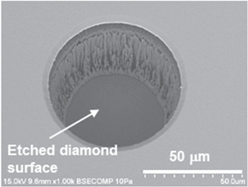
Fig. 3. SEM image of via-hole during diamond-TSV etching.
Download figure:
Standard image High-resolution imageAs shown in Fig. 4, we successfully fabricated GaN/diamond MMICs with TSVs. The chip size of the MMIC is 1.2 × 1.5 mm2, and the diameters of the TSVs are ϕ75 μm. The total gate width (Wg) of the devices was 1.44 mm (60 μm × 24) and gate to gate distance was 30 μm. We confirmed that the TSV process did not significantly affect the device characteristics such as threshold voltage, transconductance and drain current by comparing the DC characteristics of the discrete HEMTs with and without the TSV process.
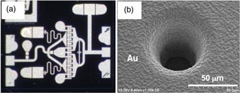
Fig. 4. GaN/diamond MMIC fabricated in this study; (a) photograph of the MMICs (front-side view), (b)SEM image of the TSV (back-side view).
Download figure:
Standard image High-resolution imageHere, the effect of heat dissipation with and without the diamond heat spreader were evaluated using test transistors. The Wg of the transistors was 0.72 mm (60 μm × 12), which was half that of the MMICs. Figure 5 shows the surface temperatures of AlGaN/GaN HEMTs as functions of the applied DC power dissipation. The channel temperature was evaluated using an infrared camera. The thermal resistance obtained from the relationship between the power dissipation and temperature was 7.2 °C W−1 in the device without diamond. In contrast, in the device with diamond, the rise in surface temperature due to power dissipation was suppressed, and the thermal resistance was 4.1 °C W−1. In the device with diamond, the thermal resistance was reduced by 43% compared with that without diamond, indicating that the heat spread efficiency of diamond was extremely high.
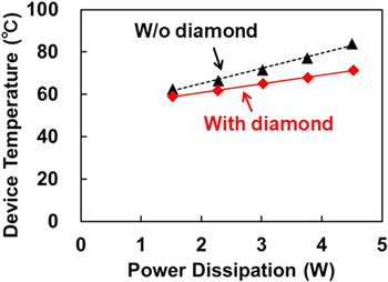
Fig. 5. (Color online) Relationship between the surface temperature of devices and power dissipation of AlGaN/GaN HEMTs measured using an infrared camera.
Download figure:
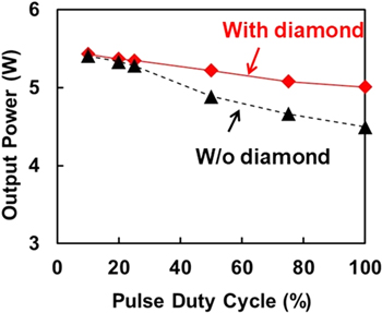
Standard image High-resolution imageThen, RF measurements of GaN MMICs on diamond at 7 GHz were performed. Wideband power amplifiers [Fig. 4 (a)] operating at 7–11 GHz were used as the MMICs. Drain bias and drain current of the MMICs were 30 V and 72 mA, respectively. Table II shows the large signal performance of the MMICs at 7 GHz. The output power at 10% duty cycle of the devices without diamond was 5.41 W, the large signal gain was 9.6 dB, and the power-added efficiency (PAE) was 32.9%. On the other hand, the output power at 10% duty cycle of the device with diamond was 5.43 W. Impedance tuners were used in order to obtain almost the same output power delivered from the MMICs with and without diamond at 10% duty cycle, which means that self-heating effect can be ignored. Figure 6 shows the output power of the MMICs as a function of the pulse duty cycle. As the pulse duty increased, the output power density of the device without diamond decreased owing to its self-heating. In contrast, in the diamond-bonded device, the output power hardly decreased even during continuous wave (CW) and high-duty pulse operations. The device characteristics with and without diamond during CW operations are as shown in Table II. The output power of MMICs without diamond at CW operation decreased to 4.50 W, whereas the output power of 5.01 W was obtained with the device on diamond. It was also shown that the degradation of PAE was suppressed by the effect of the diamond heat spreader.
Table II. Large signal performance at 7 GHz of MMICs with and without diamond heat spreader.
| 10% pulse duty | CW operation | |||
|---|---|---|---|---|
| Without diamond | With diamond | Without diamond | With diamond | |
| Output power (W) | 5.41 | 5.43 | 4.50 | 5.01 |
| Large signal gain (dB) | 9.6 | 9.0 | 9.3 | 8.7 |
| Drain efficiency (%) | 36.9 | 40.8 | 34.3 | 39.7 |
| PAE (%) | 32.9 | 35.2 | 27.2 | 33.5 |
Fig. 6. (Color online) Pulse duty dependence of the output power of the GaN MMICs with and without diamond heat spreader.
Download figure:
Standard image High-resolution image
It has been confirmed by simulation that the surface temperature of the device during CW operation is lowered by about 20 °C due to the heat dissipation effect of the diamond. As a result, the output power during CW operations was successfully increased by 11% by using the diamond heat spreader structure. Furthermore, considering the reliability of GaN devices during CW operation, 31) it can be expected that lowering the channel temperature by 20 °C will extend the lifetime by an order of magnitude. These results showed that GaN/diamond MMICs with TSVs successfully improved the heat dissipation of these devices, thus enabling high-power and high-duty operations.
Acknowledgments
We thank Y. Niida, K. Saito, M. Yamada and A. Takahashi for their support during this work. This work was partially supported by Innovative Science and Technology Initiative for Security Grant No. JPJ004596, ATLA, Japan.