

Abstract
We propose a novel fabrication technique based on the formation of a Nb protective layer on a MgB2 thin film and high-temperature post-annealing to increase the critical current density (Jc) of MgB2 films under an external magnetic field. Analyses of the crystal structure and the composition of the processed MgB2 films confirmed the suppression of the evaporation and oxidation of Mg by high-temperature annealing above 550 °C. The MgB2 film annealed at 650 °C exhibited a Jc of 1.62 MA cm−2 under 5 T, which is the highest reported value for MgB2 films, wires, and bulk samples to date.
Export citation and abstract BibTeX RIS

Content from this work may be used under the terms of the Creative Commons Attribution 4.0 license. Any further distribution of this work must maintain attribution to the author(s) and the title of the work, journal citation and DOI.
The critical temperature (Tc) of magnesium diboride (MgB2) is 39 K, 1) higher than that of conventional metallic superconductors, such as Nb–Ti and Nb3Sn. This enables the liquid-helium-free operation of MgB2 at 20 K with a suitable cryocooler or liquid-hydrogen cooling. There have been extensive studies to optimize the characteristics of MgB2 as an alternative to conventional metallic superconductors for applications in liquid-helium-free and low-cost superconducting wires. An important potential application of MgB2 is in superconducting magnets for magnetic resonance imaging systems that are widely used for noninvasive biological imaging.
Powder-in-tube (PIT) techniques, involving in situ, 2) ex situ, 3) and internal magnesium diffusion 4) processes, have been extensively explored for the convenient fabrication of superconducting wires. However, PIT techniques are based on powder sintering that results in not only a low filling factor, but also the formation of MgO between adjacent MgB2 grains, which hinders the flow of the superconducting current. 5) Consequently, the critical current density (Jc) of MgB2 wires at 20 K is lower than that of Nb–Ti wires at 4.2 K. The preparation of MgB2 has been explored using thin-film deposition techniques under vacuum, such as pulsed laser deposition, 6) molecular beam epitaxy, 7) electron beam evaporation (EBE), 8) hybrid physical-chemical vapor deposition (HPCVD), 9) radio frequency magnetron sputtering, 10) and reactive evaporation. 11) The synthesis of MgB2 under vacuum results in a high relative density and suppresses the oxidation of Mg; thus, there is an increase in the superconductivity. The Jc of MgB2 thin films is generally more than ten times higher than that of PIT-processed wires in practice. HPCVD can be utilized to fabricate high-quality MgB2 films that exhibit a self-field Jc of approximately 100 MA cm−2 at 20 K. However, the Jc of these films decreases drastically to approximately 0.5 MA cm−2, which is similar to that of PIT-processed MgB2 wires under a magnetic field of 1.5 T. It is necessary to optimize the Jc characteristics of MgB2 films under magnetic fields at 20 K to facilitate large-scale engineering applications.
In one of our previous studies, we demonstrated the effects of in situ annealing under ultrahigh vacuum (<4 × 10⁻⁷ Pa) on MgB2 thin films that were grown by EBE at a low substrate temperature of 280 °C. 12) The film that was annealed at 550 °C for 100 h exhibited a Tc of 36.7 K and an infield Jc of 0.64 MA cm−2 at 20 K under 5 T. The Tc of the film was comparable to that of PIT-processed MgB2 wires. However, the infield Jc of the film was several times higher than that of as-grown MgB2 films and several tens of times higher than that of PIT-processed MgB2 wires. These results suggested that high-temperature annealing above 550 °C can increase the infield Jc of MgB2 thin films. However, high-temperature annealing also promotes the diffusion, evaporation, and oxidation of Mg in MgB2, thereby decreasing Tc and Jc.
It is considered that the fabrication of a suitable protective layer on the MgB2 film can effectively prevent the degradation of this film during high-temperature annealing. The protective layer must not react with MgB2 during post-annealing. It should also possess a high conductivity in the low-temperature range at which the MgB2 wire is operated, so that a current flows into the copper stabilization layer, which passes through the protective layer, during the quenching of the MgB2 wire. This study demonstrates the use of Nb as a protective layer during the high-temperature annealing of MgB2 at 650 °C. Nb is commonly used as sheath material for PIT-processed MgB2 wires, and it has been reported that Nb sheaths hardly degrade the superconductivity of MgB2 at annealing temperatures below 700 °C. 13) The results showed that the Nb protective layer facilitated the post-annealing of MgB2 thin films at 650 °C. This resulted in the optimization of the Jc–B characteristics of the MgB2 thin films, and the annealed film exhibited a high Jc of 1.62 MA cm−2 at 20 K under 5 T.
The MgB2 thin film was fabricated on a single-crystalline Si substrate (20 mm × 20 mm × 0.5 mm) by EBE. The base pressure of the EBE chamber was less than 6.2 × 10⁻⁶ Pa. The substrate was heated at 270 °C using a halogen lamp heater during the deposition in the EBE chamber. The raw materials for the fabrication of the MgB2 thin films were a block of Mg (99.9%) and granular B (99.5%). The flux rates of Mg and B were independently controlled using two quartz crystal monitors, and the deposition rate of MgB2 was 0.6 nm s−1. The chemical composition was quantitatively determined by inductively coupled plasma-optical emission spectrometry. The crystalline phases in the films were determined using θ–2θ X-ray diffraction (XRD). The measurements of Jc (at 20 K under various external magnetic fields up to 6 T) and Tc were performed by a four-probe method using a physical property measurement system (Quantum Design, Inc., California, USA). The applied magnetic field was perpendicular to the film surfaces. The cross-sectional microstructures and the elemental mappings of the films were obtained by bright-field scanning transmission electron microscopy (BF-STEM) and energy-dispersive X-ray spectroscopy (EDS), respectively.
A 5 nm thick Nb layer was fabricated using an arc plasma gun in the EBE chamber after the fabrication of the MgB2 film. The Nb layer prevented the oxidation of Mg during the transfer. The sample was taken out from the EBE chamber into the atmosphere and placed in a sputtering chamber. Additionally, a 3 μm thick Nb layer was prepared to protect the MgB2 thin films during post-annealing. The post-annealing was performed after the deposition of the layers in a furnace at 450 °C, 550 °C, and 650 °C for 1 h in an atmosphere of Ar+H2 (3%) at approximately 100 Pa. Subsequently, the crystal structures, the microstructures, and the elemental mappings were obtained for the samples; additionally, the values of Jc and Tc were measured. The chemical composition of the MgB2 thin film before annealing was Mg:B = 1:1.97, which was similar to the stoichiometric composition of MgB2.
Figure 1 shows the XRD patterns of the MgB2 thin films under various post-annealing conditions. The presence of Nb (110) and MgB2 (002) peaks in the XRD pattern of the nonannealed films revealed the formation of c-axis oriented MgB2 thin films. 12) The intensity of the XRD peaks of MgB2 was low owing to the deposition of the Nb protective layer on the MgB2 film; therefore, the MgB2 (001) peak was not observed in this study. The XRD pattern of the film that was annealed at 450 °C was not significantly different from that of the nonannealed film. The XRD pattern of the film that was annealed at 550 °C exhibited the presence of not only Nb (110) and MgB2 (002) peaks but also of a weak peak at approximately 2θ = 33.5° that was assumed to be related to Nb2O5 (111). This peak was clearly visible in the XRD pattern of the film that was annealed at 650 °C. The Nb (110) peak shifted toward a low angle in the XRD pattern of the film that was annealed at 550 °C; furthermore, a small shoulder appeared on the left side of the Nb (110) peak. These changes in the XRD pattern were attributed to the formation of NbO because the NbO (111) peak was observed at 2θ = 37.9°. There were no peaks corresponding to MgO in the XRD patterns of the annealed films. The full width at half maximum (FWHM) of the MgB2 (002) peaks for the nonannealed film was 0.49°. The FWHMs of the MgB2 (002) peaks for the films that were annealed at 450 °C, 550 °C, and 650 °C were 0.40°, 0.46°, and 0.31°, respectively. These results indicated that the oxidation of MgB2 was not promoted by annealing, and there was an increase in the crystallinity of the MgB2 layers after annealing.
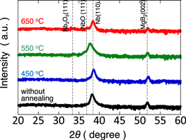
Fig. 1. (Color online) XRD patterns for the nonannealed and annealed (450 °C, 550 °C, and 650 °C) MgB2 thin films.
Download figure:
Standard image High-resolution imageFigure 2 shows cross-sectional BF-STEM images and the EDS elemental mappings (Nb, Mg, B, and O) in the annealed samples (450 °C, 550 °C, and 650 °C) comprising the Nb/MgB2/B/Si layers and EDS line profile of Mg. Each layer was clearly visible in the BF-STEM images. The thicknesses of the B, MgB2, and Nb layers were determined to be 88 nm, 193 nm, and 3 μm, respectively, using the BF-STEM images. The sizes of the columnar grains of MgB2, which were observed in the MgB2 layers, did not change with the annealing temperature. The average grain size was determined to be 36.8 nm using the cross-sectional STEM images. The results of the EDS elemental mappings indicated that the diffusion of Nb into the MgB2 layers did not occur under any annealing condition in this study. However, a diffusion of Mg from the MgB2 layers into the B layers was observed. The EDS line profile in Fig. 2(d) shows a more detailed distribution of Mg at each annealing temperature. When the annealing temperature was increased, there was an expansion of the region where Mg diffused in the B layer. A small amount of diffusion of Mg into the Nb layer was also observed; however, the amount of diffusion did not increase, even when the temperature was increased. This indicated that the Nb layer effectively suppressed the evaporation of Mg. The B distribution images revealed the presence of the B signal not only in the MgB2 and B layers but also in the Nb layer. This was attributed to the overlapping of the characteristic X-rays that were emitted from the B and Nb layers (0.1833 keV for the B Kɑ line and 0.1717 and 0.1718 keV for Nb M-lines), and we considered that there was no diffusion of B into the Nb layers. In fact, Nb sheaths in the PIT-processed MgB2 wires work well, even after heat treatment at 650 °C. 13) A clear O signal from the natural oxide film of Si was observed at the B/Si interface of the sample that was annealed at 450 °C. This sample also exhibited a weak background O signal that was spread over all layers. The sample that was annealed at 650 °C exhibited the presence of a strong O signal at the Nb/MgB2 boundary, in addition to the O signal from the natural oxide film of Si. The intensity of the B signal at the Nb/MgB2 boundary decreased in the region where the O signal was observed. This suggested the formation of an ultrathin MgO layer at the Nb/MgB2 boundary. There was no evidence of oxidation in the MgB2 layer, apart from the presence of this ultrathin MgO layer. Therefore, the Nb layer effectively protected the MgB2 layer from the effect of oxygen.
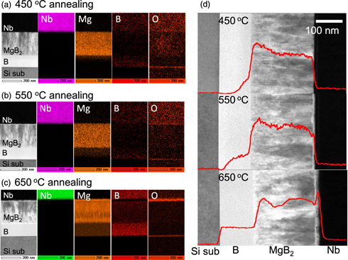
Fig. 2. (Color online) Cross-sectional bright-field STEM images and EDS elemental mappings for Nb, Mg, B, and O in the samples with Nb/MgB2/B/Si layers after annealing at (a) 450 °C, (b) 550 °C, and (c) 650 °C, and EDS line profiles of Mg at each annealing temperature.
Download figure:
Standard image High-resolution imageFigure 3 shows the temperature dependence of the resistivity of the MgB2 thin films under various annealing conditions. The resistivities of the annealed samples in the normal state were lower than the actual resistivities owing to the additional current flowing through the Nb protective layer that was not deposited on the nonannealed sample. The onset and the zero-resistivity Tc for the nonannealed sample were 35.5 K and 34.9 K, respectively. The zero-resistivity Tc for the films that were annealed at 450 °C, 550 °C, and 650 °C were 36.3, 36.8, and 37.5 K, respectively. The increase in the Tc with the increase in the annealing temperature was attributed to the increase in the crystallinity of the MgB2 layers after annealing, as proven by the XRD analysis. The Tc of the film that was annealed at 650 °C increased by 2.6 K as compared to that of the nonannealed film and was equivalent to that of the PIT-processed wires. 13) The transition widths (onset Tc–zero-resistivity Tc) of the samples that were annealed at 450 °C, 550 °C, and 650 °C were 0.3, 1.0, and 0.8 K, respectively. As shown by the XRD patterns in Fig. 1, high-temperature annealing improved the crystallinity. However, the MgB2 thin film consisted of nonuniform grains with an average grain size of about 36.8 nm, as shown in the STEM image in Fig. 2, and the degree of improvement in crystallinity is also expected to vary with each grain. Thus, the increase in the transition widths at high annealing temperatures (> = 550 °C) was attributed to the distribution of the Tc in the MgB2 layer owing to the nonuniform increase in the crystallinity after annealing.

Fig. 3. (Color online) Temperature dependence of the resistivity for the nonannealed and annealed (450 °C, 550 °C, and 650 °C) MgB2 thin films.
Download figure:
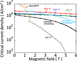
Standard image High-resolution imageFigure 4 shows the dependence of the Jc of the MgB2 films at 20 K on the magnetic fields under various annealing conditions. The results for the EBE-prepared MgB2 film that was annealed in vacuum, 12) the PIT-processed MgB2 wire, 13) and the HPCVD-prepared MgB2 film 14) are also plotted in the figure to facilitate comparison. In all data, the magnetic fields were applied perpendicular to the film surfaces. The Jc of the nonannealed MgB2 film in a self-magnetic field (1.65 MA cm−2) was almost identical to that of the MgB2 films that were annealed at 450 °C and 550 °C in the present experiment. There was a decrease in the Jc of the nonannealed film to 0.18 MA cm−2, which was approximately 90% lower than that in the self-magnetic field under a magnetic field of 5 T. The decrease in the Jc of the annealed sample under a magnetic field of 5 T was approximately 40%, which was significantly lower than that of the nonannealed sample. The MgB2 film that was annealed at 650 °C exhibited a Jc of 1.62 MA cm−2 at 20 K under 5 T. This was not only more than 2.5 times higher than the previous highest Jc of 0.64 MA cm−2 for the EBE-prepared MgB2 films that were annealed at 550 °C in vacuum 12) but also more than 100 times higher than the Jc for the PIT-processed wires. 13)
Fig. 4. (Color online) Magnetic-field dependence of the Jc at 20 K for the nonannealed and annealed (450 °C, 550 °C, and 650 °C) MgB2 thin films. The results for the EBE-prepared MgB2 film that was annealed in vacuum (light blue dotted line), 12) the PIT-processed MgB2 wire (gray dotted line), 13) and the HPCVD-prepared MgB2 film (orange dotted line) 14) are also plotted for comparison. In all data, the magnetic fields were applied perpendicular to the film surfaces.
Download figure:
Standard image High-resolution image
The results of our study demonstrated that high-temperature annealing and the Nb protective layer significantly increased the Jc of the EBE-prepared MgB2 thin films under high magnetic fields. The reasons for the high Jc can be explained as follows. The values of Tc and Jc in a self-magnetic field for the EBE-prepared films in this study were lower than those for HPCVD-prepared films. This was attributed to the smaller grains in the EBE-prepared films as compared to those in HPCVD-prepared films and the formation of a thin MgO wall with a thickness of several nanometers around each grain in the EBE films. 12) Furthermore, the cross-sectional area of the superconducting channels was only a few tens of percent of that in an ideal superconducting material. The MgO around the grains acted as pinning centers and increased the Jc under high magnetic fields. 15) To increase Jc under an external magnetic field, it is necessary to increase the crystallinity of MgB2 inside the small grains and improve Tc without forming MgO. Although high-temperature annealing above 550 °C is effective in improving Tc, it is considered to be difficult owing to the oxidation and evaporation of Mg. However, the deposition of a 3 μm thick Nb protective layer in this study effectively prevented the oxidation and evaporation of Mg at high annealing temperatures. The annealing improved Tc and facilitated flux-pinning in the grain boundaries without inducing a deterioration in the superconductivity. Thus, there was an increase in the Jc of the thin films under magnetic fields. The results of the study indicated that the performance of the fabricated MgB2 films under external magnetic fields was optimized by simple post-annealing.
To summarize, we deposited a Nb protective layer on the MgB2 thin films to suppress the evaporation and oxidation of Mg. Furthermore, the effects of the post-annealing treatment on the Jc and Tc of the MgB2 films were examined. The fabrication of the Nb protective layer and the annealing at 450 °C, 550 °C, and 650 °C resulted in an increase in the Tc and Jc of the MgB2 films. The film that was annealed at 650 °C exhibited a Jc of 1.62 MA cm−2 at 20 K under 5 T, which was more than 100 times higher than the Jc of PIT-processed wires. The results confirmed the efficacy of the fabrication technique in this study for the realization of MgB2-based conductors for practical superconducting applications at 20 K under external magnetic fields.