
Abstract
The effects of field cycling of Al0.78Sc0.22N capacitors on ferroelectric properties are investigated. In the first hundreds of switching cycles, the reduction in the switching voltage was observed, possibly due to the formation of nitrogen-vacancy to facilitate the atom displacements. With further switching cycles, fatigue effect was observed, especially for domains with low switching voltage. The leakage current analysis indicates continuous downward band bending with the number of switching cycles, effectively reducing the Schottky barrier height for electrons. The breakdown of Al0.78Sc0.22N films is triggered by the Joule heat due to excessive leakage current. The mechanism is in contrast to conventional ferroelectric materials, where the breakdown is triggered by Joule heat at the local conductive filaments.
Export citation and abstract BibTeX RIS
1. Introduction
Artificial intelligence (AI), deep learning, and machine learning have been important topics in many areas. 1–4) All these technologies need to operate at high speed with low power consumption. Computation in memory (CiM) is now important hardware to make a multiply-accumulation process with very fast speed with reduced power consumption thanks to its massive parallel operations. 5–10) The usage of nonvolatile memories in CiM is an effective way to reduce power consumption while improving the speed of the operation. Among various nonvolatile memories, including magnetic, resistive, and ferroelectric random-access-memories (RAMs), ferroelectric memory provides energy-efficient edge computing thanks to its electric field operation. 6–10) A CiM device with ferroelectric field-effective transistors (FETs) was demonstrated in 2018. 6)
The performance of ferroelectric FETs is dominated by the characteristic of the ferroelectric materials. Ferroelectric HfO2 gate dielectrics have been used as their ferroelectricity remains even in the thickness range below 10 nm. 11) Moreover, thanks to its compatibility with the conventional CMOS fabrication process, a 3D NAND-type ferroelectric FET array and nonvolatile memory applications have been demonstrated. 12–14) However, there is still some issue for ferroelectric HfO2 to be solved.
One of the issues is the switching cycle. A typical endurance cycle of ferroelectric HfO2 capacitors before dielectric breakdown is around 109 cycles or less. 15,16) The switching cycles can be improved to some extent by the capping process or other element incorporation, and the high endurance of 1011 cycles has been successfully demonstrated. It is reported that oxygen vacancies are formed during the field cycling, and once the chain of oxygen vacancies occurs, a local current path will be formed between the electrodes. 17–19) Once the conductance of the current path becomes high, the excess Joule heat at the path will trigger the breakdown of the device.
Recently, a new ferroelectric material AlScN was found in 2019. 20) A large remnant polarization (Pr) of about 100 μC cm−2 with a box-like profile in the hysteresis curve is attractive for memory devices. The origin of the large polarization comes from the wurtzite structure of the AlScN film. The switching mechanism is explained by the movement of the nitrogen atom, changing the surface between metal and nitrogen faces. The ferroelectric and electrical properties can be adjusted by controlling the content of Sc from 10% to 40%, giving flexibility to memory design. 21–24) Although thickness scaling showed degradation in the thin region, the ferroelectricity is kept for a thickness less than 10 nm. 25–27) Furthermore, ferroelectric AlScN films with the room-temperature process are attractive for embedded CiM applications. 28) Although many works are focused on composition or thickness-dependent ferroelectric properties, there are few works on endurance, including field cycling change and dielectric breakdown. 29) In this paper, we measured the field cycling change, especially the change at the near-interface region, of 50 nm thick Al0.78Sc0.22N films and proposed a model for the dielectric breakdown.
2. Device fabrication and measurement
A 50 nm thick ferroelectric Al0.78Sc0.22N film with top and bottom TiN layers were deposited in situ on an n+Si substrate in the same chamber by reactive sputtering at a substrate temperature of 400 °C. The top electrode was patterned by wet etching to form electrodes. The detailed process and film characteristics are reported in Refs. 20,25,28. The Pr and the coercive field (Ec) were >100 μC cm−2 and 5.3 MV cm−1, respectively. The breakdown field was about 8.1 MV cm−1. A columnar structure is confirmed by transmission electron microscope (TEM) and X-ray rocking curve. An electrode size of 56 × 56 μm2 was used for measurements.
Sinusoidal waves with a voltage amplitude (Vamp) of 28 V, corresponding to an electric field of 5.6 MV cm−1, at 2 kHz were applied to the top electrode. The voltage application was ended by using a positive voltage to the top electrode, resulting in upward polarization of the devices. Note that the Al0.78Sc0.22N layer is already polarized in an upward direction after deposition. The numbers of switching cycles were set to 102–105 cycles. The field cycling test or the switching endurance of the ferroelectric AlScN capacitors is evaluated by capacitance–voltage (C–V), positive-up negative-down (PUND) measurement with a pulse height (Vpulse) of either 26 or 28 V, with a pulse width of 8 μs. The near-interface property change on the number of switching cycles is monitored by leakage current analyses by applying a positive voltage to the top electrode.
3. Field cycling behavior of AlScN capacitor
Double sweep C–V curves of the capacitors after different numbers of switching cycles from 0 to −28 V, in the direction to induce the polarization reversal of the AlScN film, are shown in Fig. 1. The devices with fresh and 102 switching cycles showed little difference, showing a peak capacitance at −22 V with a sudden drop at further negative voltage application, suggesting the ferroelectric switching. The crossover capacitance between the forward and backward sweeping was at −9.4 V, indicating the presence of imprint effect in the capacitor. With larger numbers of switching cycles, another capacitance peak start to appear at −16 V with a gradual capacitance decrease for the first one at −22 V. The transition in the voltage at peak capacitance did not complete with a switching cycle up to 105 times, indicating that high voltage switching components remain in the film. The increase in the capacitance of the device with 105 switching cycles at −22 V is due to leakage current as the dissipation factor (tan δ) of the measurements was more than 4. The increase in the leakage current will be explained later. The capacitance crossover shifted to a positive direction from −9.4 V to −3.4 V, but since the high switching voltages remain, the shift is not due to negative charge trapping in the film. Note that the voltage at the peak capacitance in the positive voltage region showed a slight reduction with the number of cycles. This fact also supports the change in the switching voltage in the negative voltage region. It is interesting to note that the large change in the voltage at the peak capacitances is only observed in the negative voltage sweep. Although the physical reason is still unclear, there should be a physical asymmetry in the film.
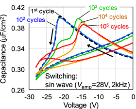
Fig. 1. (Color online) C–V curves of the devices with different switching cycles.
Download figure:
Standard image High-resolution imageThe Pr of the capacitors on the number of switching cycles, measured at different Vpulse is shown in Fig. 2. A slight wake-up effect is observed in the first 102 cycles for Vpulse of 28 V, changing the Pr from the initial 89 to 95 μC cm−2. Further switching cycles more than 104 times resulted in a slight reduction in Pr, indicating the fatigue effect. For the Pr obtained by Vpulse of 26 V, the initial value was comparable to that of 28 V, thus the applied voltage was sufficiently high for the switching voltage. However, a severe fatigue effect was observed after 104 switching cycles without presenting the wake-up effect. As the difference in Pr between the two voltage pulses represents the presence of components with a switching voltage of higher than 26 V, the increase in the gap infers some portion of the ferroelectric domains, especially with low switching voltage components, are pinned by the switching cycles, presumably due to electron trapping.
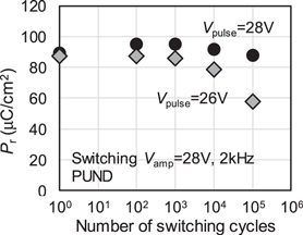
Fig. 2. Pr obtained at two different pulse voltages after the number of switching cycles.
Download figure:
Standard image High-resolution image4. Near-interface region change by switching cycles
The near-interface region change upon ferroelectric switching can be deduced from leakage current analysis. It is reported that a high concentration of VN already exists in the film at an as-deposited state; thus, downward band bending increases the leakage current. It is also reported that the concentration of VN at the near-interface region increases by the first ferroelectric switching. 30) We adopt this method to capture the physical image of the near-interface region change by field cycling. The Schottky plot of the leakage current (J) of devices with different switching cycles at fresh and after 103 and 105 switching cycles measured at 40 °C are shown in Fig. 3. All the leakage current followed the Schottky emission model with slightly different parameters. This finding indicates that electrons are not conducting locally but rather uniform from the electrode. The leakage current firstly increases with 103 cycles and then reduces with 105 switching cycles.
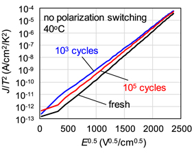
Fig. 3. (Color online) Schottky plot of the devices at fresh and after switching cycle of 103 and 105 times.
Download figure:
Standard image High-resolution imageThe Schottky emission model with a tunneling barrier at the Al0.78Sc0.22N/metal interface can be expressed as follows,
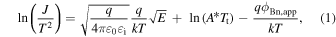
where E, T, q, k, ε0, εi, A*, and ϕBn,app are the electric field, absolute temperature, elementary charge, Boltzmann constant, vacuum permittivity, optical dielectric constant, effective Richardson constant, and apparent Schottky barrier height to electron, respectively. By introducing a rectangular-shape tunneling barrier, the tunneling probability (Tt), can be expressed as

where m*, ħ, ϕBn, d is the effective electron mass, reduced Planks constant, Schottky barrier height for an electron at Al0.78Sc0.22N/metal interface, and tunneling distance, respectively. 31) The physical origin of the tunneling barrier is explained by the downward band bending at the interface, presumably due to the presence of charged VN.
The εi values were extracted from the slope of the Schottky plot and are shown in Fig. 4. The initial value of 2.8 for fresh devices showed a gradual increase up to 3.5 after 103 switching cycles. Note that the obtained εi values are the dielectric constant at high frequency, which is the square of the refractive index, as the transition of electrons through the interface is shorter than the dielectric response. Therefore, by the dielectric relaxation of the ionic polarization, the εi values are generally 1/4–1/10 of the static dielectric constant. 32) The increase in εi can be understood from the creation of VN near the interface. On the other hand, further switching cycles results in the reduction in εi down to 2.1, less than the value of the fresh device. As the switching is performed at a high electric field of 5.6 MV cm−1, the atomic rearrangement, possibly including the compositional change, at the near-interface of the Al0.78Sc0.22N layer can likely happen.
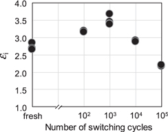
Fig. 4. Extracted εi shows a gradual increase and roll-off behavior with the number of switching cycles.
Download figure:
Standard image High-resolution imageBy taking the intercept in the Schottky plot measured at a different temperature, as shown in Fig. 5, the ϕBn,app can be obtained. The ϕBn,app was found to decrease continuously with the switching cycle from 0.59 to 0.27 eV after 105 switching cycles.
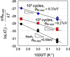
Fig. 5. (Color online) Intercept in the Schottky plot measured at different temperatures for fresh and after switching for 103 and 105 times.
Download figure:
Standard image High-resolution imageAlthough A* of Al1−x Scx N films is not reported, we can assume an A* for Al0.78Sc0.22N films ranges from 10 to 50 A cm−2 K−2. Therefore, in the calculation, an A* of 50 A cm−2 K−2, 33,34) which corresponds to an m* of 0.42m0, where m0 is the mass of electrons, is used. We also adopted the ϕBn to be 2.3 eV, 22) which was extracted by X-ray photoelectron spectroscopy. The extracted ϕBn,app, A*Tt, and d are summarized in Fig. 6. The error bars represent the extraction accuracy from the data taken from Fig. 5. The ϕBn,app, and A*Tt continuously decrease with the number of cycles. As the leakage current is the balance between the ϕBn,app, and A*Tt as is expressed in Eq. (1), the increase and decrease behavior observed in Fig. 3 with switching cycles can be understood. The d, on the other hand, continuously increases with the number of switching from 4 to 6 nm, indicating that the downward bending becomes much steeper with switching. This finding indicates that the near-interface as deep as 6 nm can be modified by ferroelectric switching of Al0.78Sc0.22N films.
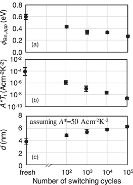
Fig. 6. (a) ϕBn,app (b) A*Tt and (c) d on the number of switching cycles.
Download figure:
Standard image High-resolution image5. Film aging upon switching cycles and breakdown
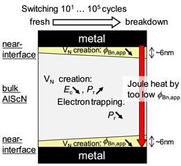
Based on the obtained results, the picture of the physical phenomena in the bulk and at the near-interface region induced by the switching cycle test is illustrated in Fig. 7. A large number of VN already exists in the film at as-deposited conditions. With hundreds of switching cycles, VN is created both in the bulk and at the near-interface region. The bulk VN creation contributes to facilitating the displacement of N atoms, creating ferroelectric domains with a low Ec. Those formed in the near-interface region bend down the conduction band to increase the tunneling probability of electrons from the electrode. With further switching cycles, electron trapping might take place in the bulk Al0.78Sc0.22N to pin the ferroelectric domains, especially from low Ec components, reducing the Pr. In the near-interface region, continuous creation of VN results in further reducing the ϕBn,app. The near-interface regions extend as deep as 6 nm with 105 switching cycles. Once the leakage current becomes sufficiently high, the capacitor brake down by excessive Joule heat. We should note that the breakdown mechanism is different from other PZT-based or HfO2-based ferroelectric materials, where conductive filaments formation to bridge the electrodes trigger the breakdown.
Fig. 7. (Color online) An illustration model of the reduction on the apparent Schottky barrier height and the increase in the tunnel distance after the cycling test.
Download figure:
Standard image High-resolution image
6. Conclusions
The field cycling of ferroelectric Al0.78Sc0.22N capacitors revealed the reduction in the switching voltage, possibly due to the formation of VN to facilitate the movement of atoms. Also, fatigue effect was observed after switching for 103 cycles, presumably due to electron trapping to pin the ferroelectric domains. The apparent Schottky barrier height was continuously reduced with switching by downward bending the energy band to tunnel the electrons. The breakdown of Al0.78Sc0.22N films is triggered by the Joule heat due to excessive reduced barrier height. The mechanism is in contrast to conventional ferroelectric materials, where the breakdown is triggered by local conductive filaments.
Acknowledgments
This work is partially supported by the Murata Science Foundation. This work was financially supported by the "Center for the Semiconductor Technology Research" from The Featured Areas Research Center Program within the framework of the Higher Education Sprout Project by the Ministry of Education (MOE) in Taiwan. Also supported in part by the Ministry of Science and Technology, Taiwan, under Grant MOST 109-2634-F-009-027.