Article

Design and Experimental Verification of Voltage Measurement Circuits Based on Linear Optocouplers with Galvanic Isolation for Battery Management Systems

1
School of Engineering, Computing and Mathematics, Oxford Brookes University, Wheatley campus, Oxford OX33 1HX, UK
2
Faculty of Engineering and the Environment, University of Southampton, University Road, SO17 1BJ Southampton, UK
*
Author to whom correspondence should be addressed.
World Electr. Veh. J. 2019, 10(4), 59; https://doi.org/10.3390/wevj10040059
Submission received: 20 July 2019 / Revised: 15 September 2019 / Accepted: 18 September 2019 / Published: 23 September 2019
(This article belongs to the Special Issue Power Electronics Subsystems)

Abstract

:
A battery management system (BMS) design, based on linear optocouplers for Lithium-ion battery cells for automotive and stationary applications is proposed. The critical parts of a BMS are the input voltages and currents measurement circuits. In this design, they include linear optocouplers for galvanic isolation between the battery pack and the BMS. Optocouplers based on AlGaAs light emitted diodes (LED) and PIN photodiode with external operational amplifiers are used. The design features linear characteristics, to ensure the accuracy of the measurements. The suggested approach is based on graphical data digitalizing, which gives the precise values for the most sensitive parameters: photocurrent, normalized and transferred servo gain and helps the calculation procedure to be automated with MATLAB scripts. Several mathematical methods in the analysis are used in order for the necessary equations to be derived. The results are experimentally verified with prototypes.

1. Introduction

The battery management systems (BMS) are a central part of the on-board vehicles battery packs and battery packs for stationary applications. They are responsible for the control of the charging and discharging process, battery cell equalisation, state of charge (SoC) estimation, etc., and due to their importance, many papers have been recently published. The major focus is given to the measurement and protection techniques, battery technologies, battery management algorithms, battery cell equalisation, SoC estimation, etc. In [1,2] advanced prototypes are investigated but the details of the electronic circuits design procedures are not presented. Publications [3,4] offer meticulous design procedures for BMS with fault-tolerant capability, battery protection and monitoring algorithms with advance aging battery models. The results reviewed present basic features of the current BMS systems and can be used for future research. In [5] implementation of BMS for emergency light with a real-time data acquisition system is presented. Although several optocouplers for general use are implemented for safety reasons, thus implementing galvanic isolation, this research is not focused on the use of optocouplers. Another interesting solution [6] presents an energy storage system with several components: Lithium-ion battery pack, ultracapacitors and fuel cells, working on high AC and DC voltages. Here, the system is well presented in a simulation environment, achieving good performance and efficiency, but the connection to the power management system is not given as hardware implementation.
The thermal management as a BMS future is investigated from papers [7,8,9], with interesting simulation and experimental results, including a fast battery charge mode. The obtained results show that the suggested circuit for galvanic isolation does not affect the thermal measurement modules and their correct operation as they are separated from the voltage measurement circuits.
Publications [10,11,12] describe different approaches to BMS design, analyses, and experimental verifications. They contain valuable data but the design methodologies used can provoke some problems, which have been identified during this research. For example, the direct connection between the developed BMS and the battery pack can cause overvoltage ripples during fast battery charge which can damage the used ASIC (application specific integral circuits) or microcontrollers. The entire measurement process can suffer from noise disturbance and ripple voltage injected from switch mode battery chargers, which at that stage also can be under development. That compromises the BMS precision and prevents its successful experimental verification. The better safety level is desirable during the research phase, especially for projects with high voltage battery packs. The analysis of these problems shows that they can be avoided, during the BMS development process or its normal exploitation, by implementing an additional galvanic isolation stage between the battery pack and BMS.
Good reviews and comparative analysis of BMS architectures and application of Lithium-ion cells equivalent circuits are offered in [13,14,15,16,17]. From these, the basic requirements for the presented design, such as precision, voltage ranges, and battery pack structure have been obtained. In [14] important safety issues are described and a BMS with fuses between the battery pack and the ASIC is suggested. Potentially, an implementation of galvanic isolated optocoupler circuits instead of or together with the fuses would increase the safety level and reliability of the entire system.
Another group of articles [18,19,20,21] offers valuable research focused on battery equalization methods as part of BMS and state of charge estimation. From analysed circuits, it can be concluded that the suggested galvanic isolation would benefit from the application of the conventional battery equalization methods, thus an alternative solution is to be found. Although the battery cell equalization technologies are not an object of this research, the converter presented in [22] has been used in the current study. The described flyback converter with primary current sensing can be applied for a battery pack with galvanically isolated cells from its BMS.
Most of the current solutions use ASICs for BMS, connected to microcontrollers which are the central control system for the automotive or stationary battery packs. Such architectures are well presented in [23], where a high voltage DC solution is suggested, or in the manufacturer’s manual [24], which shows some important BMS concepts. Usually, for the conventional BMS different ASICs such as: Renesans—ISL94202 [25], Linear—LTC6802-2 [26], Texas Instruments—BQ76920 [27], NXP—MC33771 [28], Maxim Integrated—MAX11068 [29] and many others are available currently on the market. Their thorough review is given in [30]. The same source gives advice about their application and application (electronic circuits), which have been utilised in the present work.
Galvanic isolation used as a part of the battery pack and BMS in [31,32,33] is investigated only as part of the voltage equalization system or the additional power supply modules. The battery balancing capacitors in [31] are commutated with electric switches controlled by electromagnetic relays. A similar solution is found in [32], where the BMS for motorcycles is implemented using the same mechanical contacts, but the details of voltage measurement modules are not given. In [33] several circuits with isolated power supply and communication system are given, but only as general block diagrams.
The necessity of galvanic isolation can be assumed as a mandatory requirement or at least a highly desirable feature in the following cases:
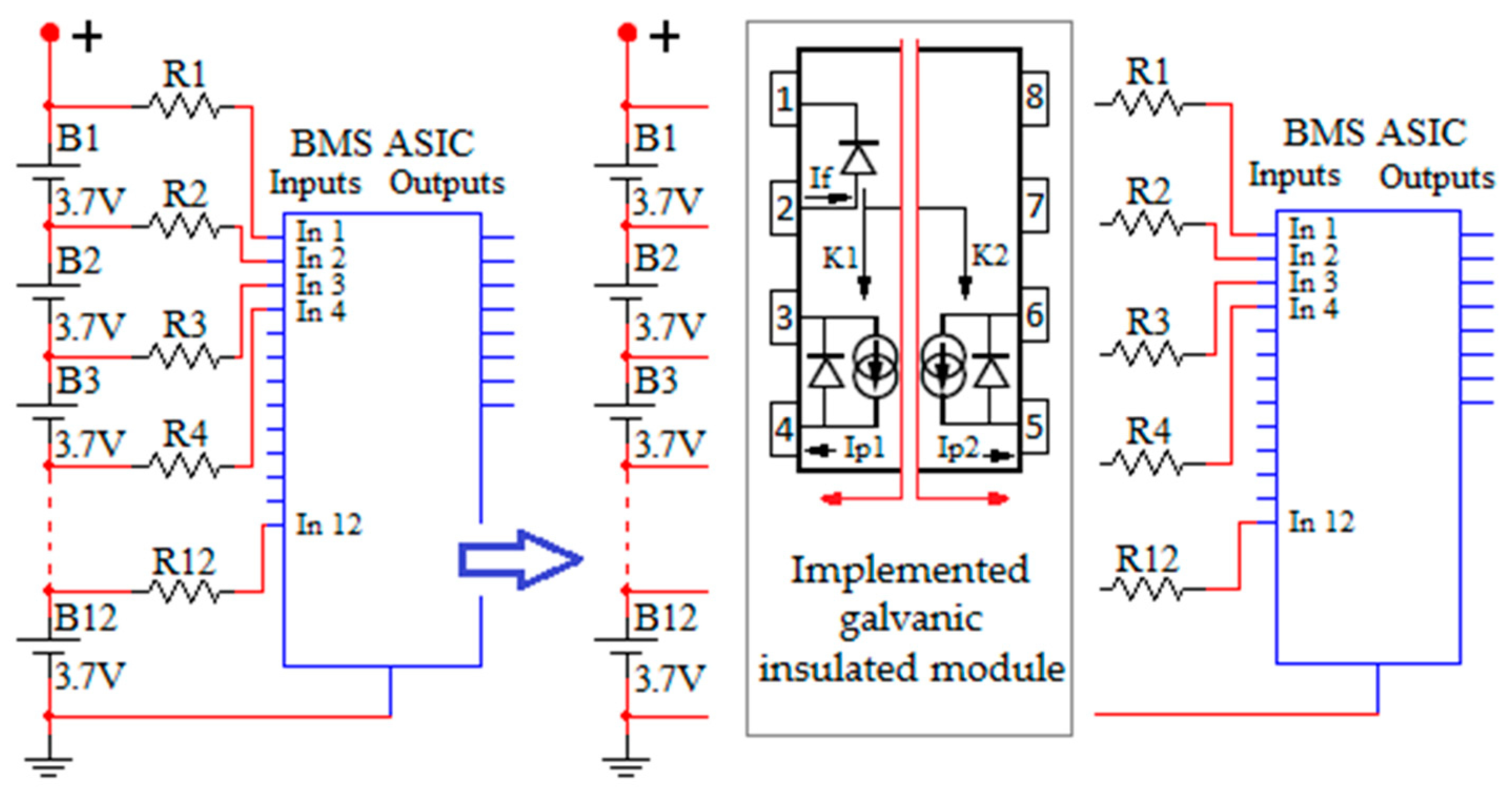
  • During the development process of BMS with battery chargers and converters for automotive and stationary applications. Due to health and safety requirements, the laboratory experimental setup must have galvanic isolation between the high voltage battery pack, and the human interface devices. Additionally, the development process based on galvanically isolated subsystems gives bigger flexibility for problem-solving, as it helps the different sources of noises, voltage ripples, overvoltages, etc. to be localised.
  • For automotive and stationary applications where two grounds of two different systems, i.e., charger/converter and BMS/control system must be separated. Permanent galvanic isolation in exploitation can be required for systems with high EMI (electromagnetic interference), electric noise, etc.
  • In order for all on-board automotive electronics requirements given in safety standards to be met, i.e., safety, reliability, robustness, maintainability, and testability, (e.g., ISO-26262).
The conducted literature research [1,2,3,4,5,6,7,8,9,10,11,12,13,14,15,16,17,18,19,20,21,22,23,24,25,26,27,28,29,30,31,32,33] shows that the opportunities for galvanic isolation between battery packs and BMS are not presented fully enough as the necessary hardware implementations of electronic circuits, design and experimental verifications. Thorough research is necessary for a technical solution to be reviewed, including electronic circuit based on available on the market low-cost components, design procedure with mathematical apparatus which is capable of giving the desired precision and experimental setup proving the base conception.
This research is focused on the input BMS voltage measurement modules with complicit galvanic isolation implemented through several types of linear optocouplers. The structure is based on AlGaAs light emitted diodes (LED) and PIN photodiodes. Such linear optocouplers are offered from different manufacturers, for example, Vishay [34]–IL300 [35,36]; Broadcom Inc. [37]–HCNR200 [38] and HCNR201 [39]; IXYS [40]–LOC110 [41], LOC111 [42], LOC112 [43] and LOC117 [44]; IXYS—dual linear optocouplers LOC210 [45] and LOC211 [46]. Their parameters are given in datasheets in graphical and numerical forms for general purposes, which means that their application in the current context must be investigated. The linear optocouplers have a high rate of galvanic isolation, usually 3–5 kV, low leakage current, high reliability, wide bandwidth, compatibility with standards IEC 60747-17 (VDE 0884-11) and EN/IEC 60950-1, low THDs, high gain stability in wide temperature range, low input-output capacity and low power consumption. Due to all these advantages, their applications are in medical electronics, telecommunications, power supply feedbacks, etc. This shows that for the suggested BMS, high robustness and accuracy can be expected, supported by a precise design procedure.
The aim of this research is to devise a specialised design procedure for BMS using galvanic isolated voltage measurement modules, based on linear optocouplers to be selected, experimental modules to be built and experimentally verified. It is derived from optocouplers general datasheet and manufacturers’ manuals [34,35,36,37,38,39,40,41,42,43,44,45,46]. Considerable attention has been applied to the voltage mismatch between the input and output voltages, which compromises the measurement precision. This problem has been minimised using several techniques: digitising graphical data, deriving system equations with trend analysis, designing the suggested circuit, specifying the minimum power supply voltage in order for voltage saturation to be avoided and verification with experiments.
The proposed concept is given in Figure 1. Additional modules are integrated between the battery pack and the input of the used ASIC. The successful design of the necessary modules requires their parameters to be calculated according to the input voltage, in this case, Lithium-ion battery cells within range 2–4.2 V, hence precise research focused exactly on such electronic circuit is necessary. Eventually, the expected results can be defined as the following requirements: the voltage mismatch must be reduced to 0.5% or under 10 mV for the entire Lithium-ion voltage range; fast enough response with small propagation delay; stable work under charge and discharge conditions; suitable for automotive applications.
The presented work is organised in the following order: Section 2 shows the analysis of the proposed circuits with a short explanation of their operation and the most probable problems that must be solved. The design procedure is given in Section 3, supported by the necessary mathematical apparatus. Section 4 shows the experimental verification with three experimental models produced. The conclusions are summarised in Section 5 and several MATLAB scripts are included.

2. Analysis

The proposed circuit for voltage measurement, used as the galvanic isolated input voltage sensors of a BMS, is shown in Figure 2. The linear characteristics are expressed in the linear proportionality between the input voltage, in this case, the measured battery cell voltage, and the output voltage, or the voltage transferred to the ASIC or microcontroller. This circuit is simple enough and does not have drift problems, which makes it a good choice for input BMS voltage galvanic isolated sensors.
During this research, a potential problem has been identified. As an example, Figure 2 shows the experimental graph including input (1) and output (2) with a significant mismatch on the right side, hence significant voltage error. In a system with ideal proportionality, adjusted at 1:1, these voltage plots are supposed to align perfectly over the entire range. However, the experiment shows 3.8 V on the last value instead of 4.2 V giving a relative error of 11.6%. Such a result can be considered as highly inaccurate and requires an appropriate solution to be found. As the linearity of these optocouplers is high enough, given by most manufacturers at 0.01%, it can be assumed that the mismatch shown in Figure 2 is caused by several other factors:
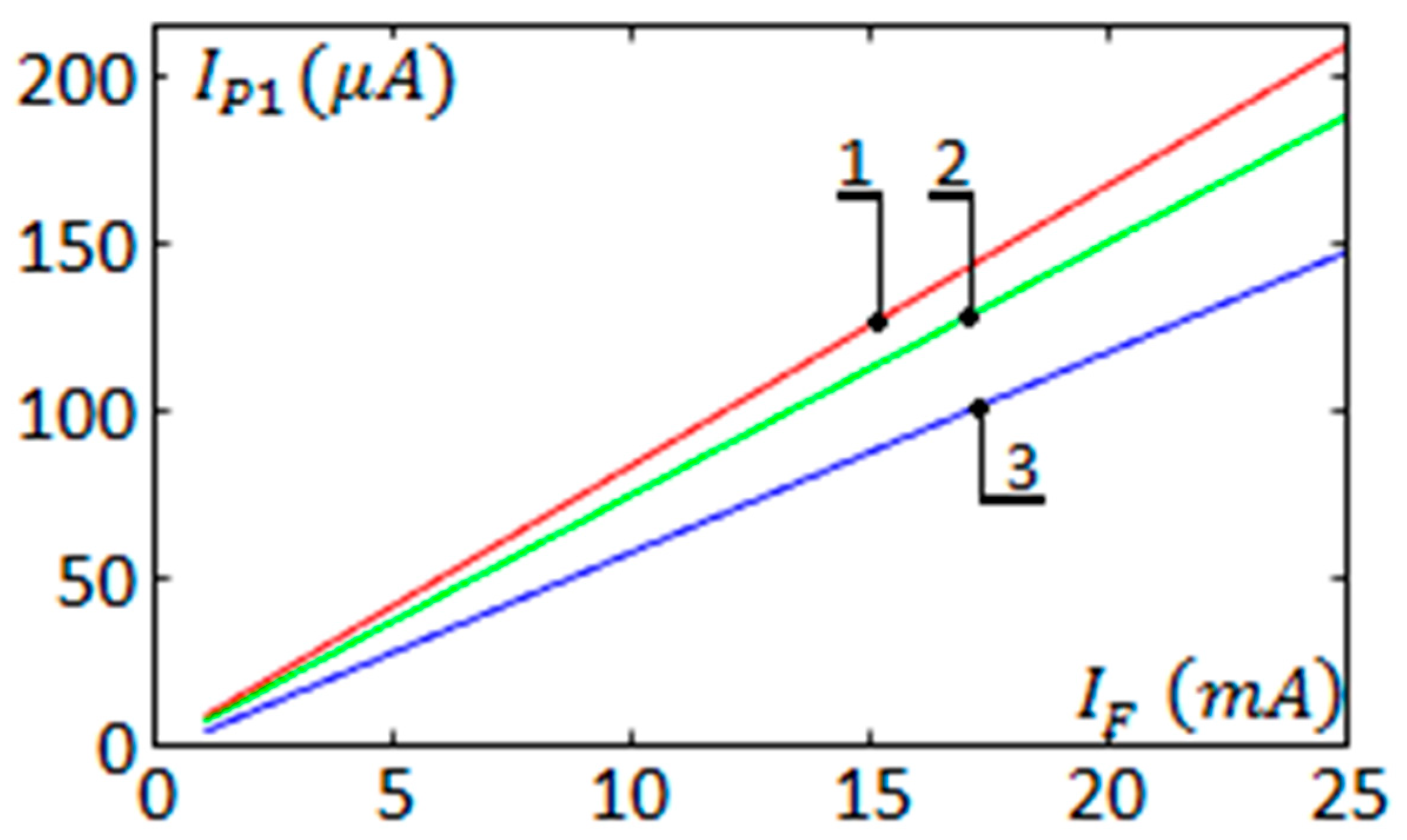
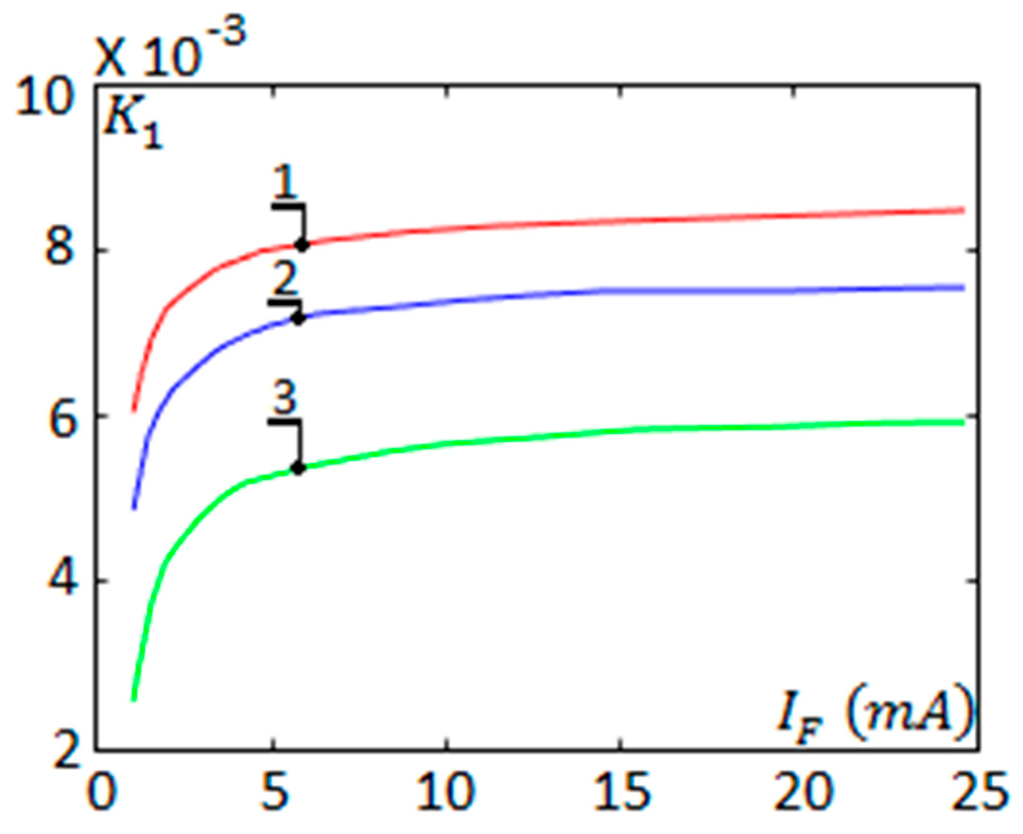
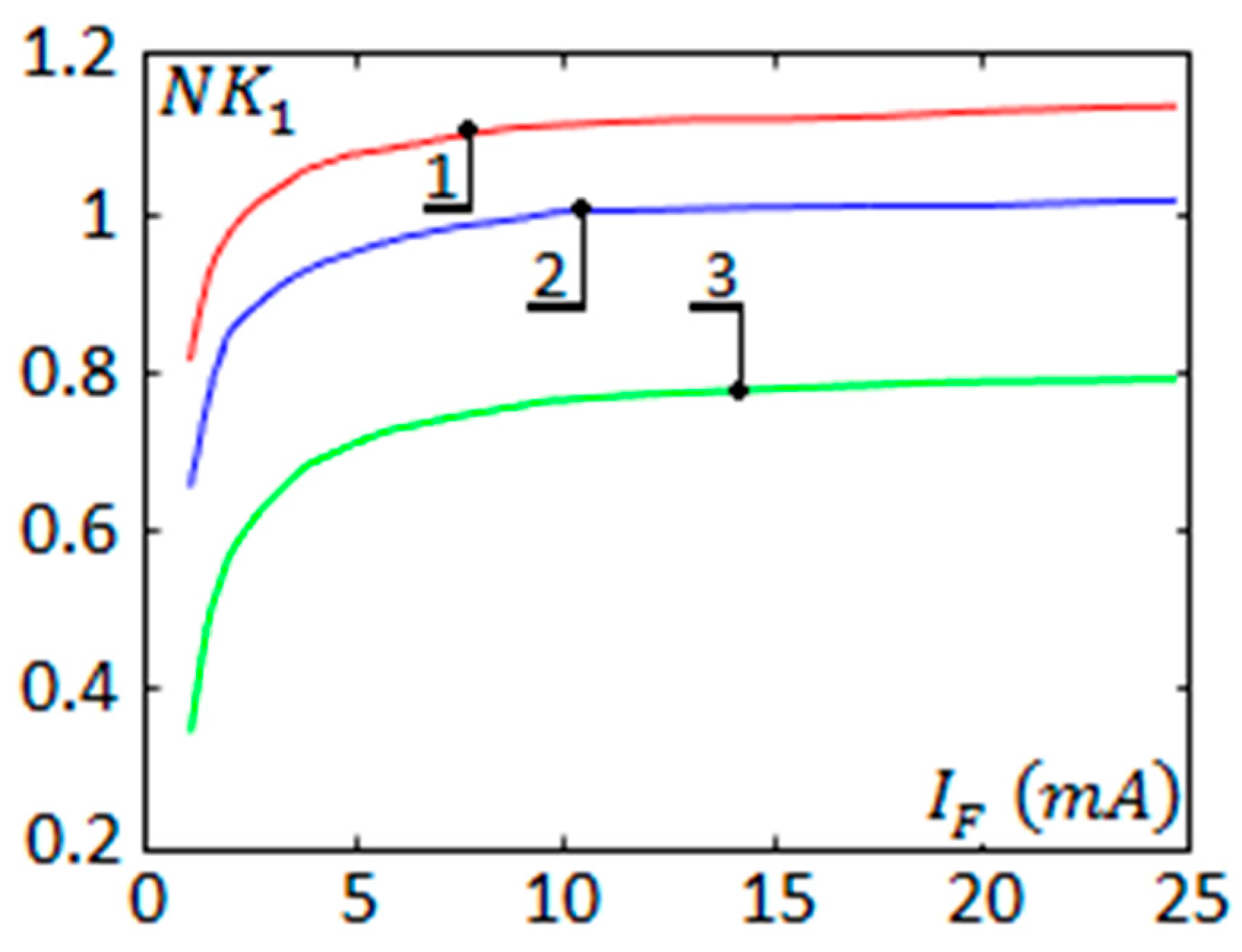
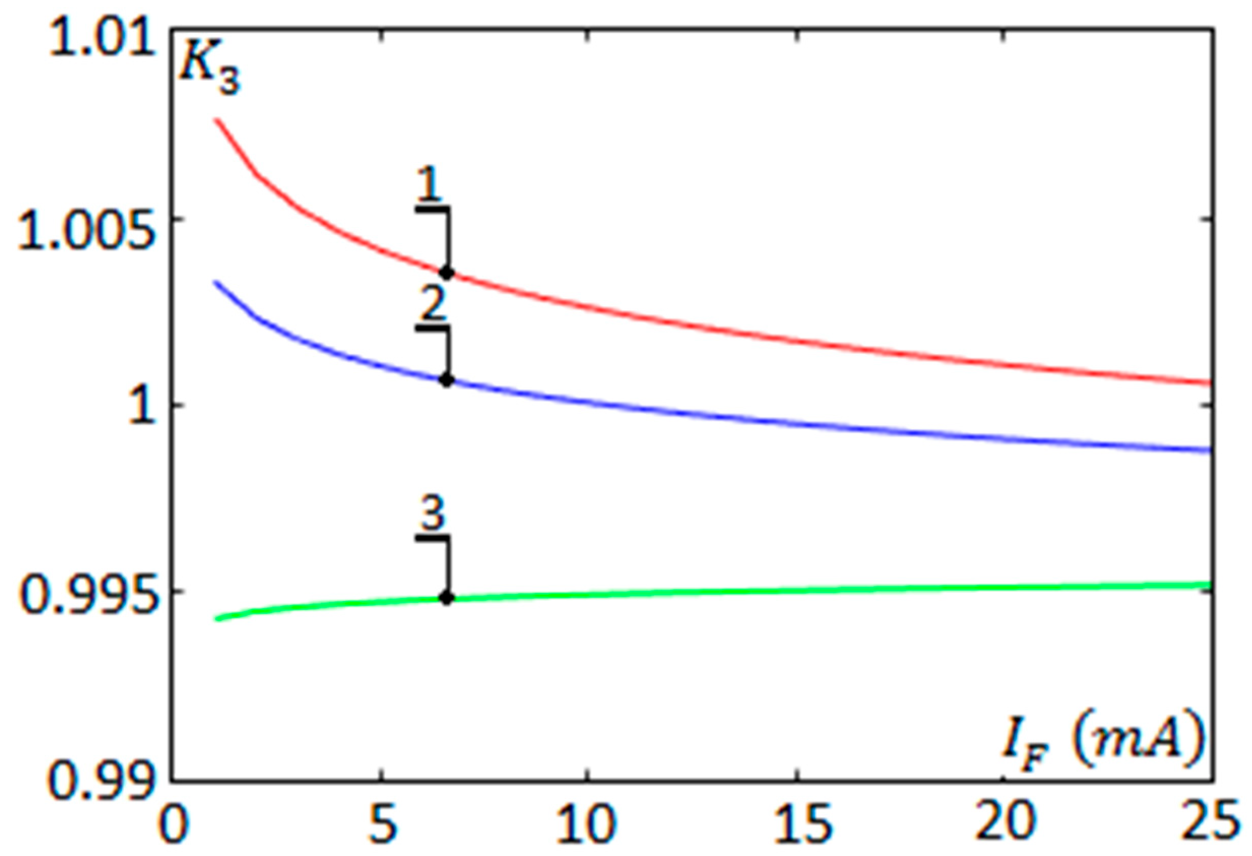
  • Imprecise values for the most sensitive parameters as gains, LED current and photocurrent, chosen directly from diagrams during the design procedure. These variables are usually given graphically in the manufacturers’ datasheets, but some of them do not have a satisfactory resolution which in this case leads to imprecise selection and eventually wrong calculations. This problem can be addressed with graphical data digitising, which is supposed to give more precise data.
  • Input voltage ranges, which must be described for the specific application. In this case, the voltage of most Lithium-ion cells is set on minimum cut-off 2.2 V, nominal 3.7 V, and maximum 4.2 V during the charging process. This problem requires a design procedure to be written and experimentally verified exactly for this case.
  • The power supply voltage for the primary and secondary side operational amplifiers must be higher than the measurement input voltage, i.e., the cell battery voltage. Within the entire range of amplification, saturation must be avoided. Here, despite the initial desire for the power supply voltage to be as low as possible in order to reduce the power losses, the minimum possible supply voltage will depend on the maximum input voltage.
The most important parameters reflecting on the sensitivity of these types of optocouplers can be given as an average for their respective ranges: servo gain, for certain temperature, varies for example between 0.003–0.005; normalized servo gain, for example between 0.6–0.7; I L E D : LED current in range 1–30 mA, but according to the manufacturers [34,37,40] requirements the best linearity can be achieved in range 5–25 mA; photocurrent between 50–100 μA.
The core of the presented circuit is the primary side feedback between the op-amp U1 and the linear optocoupler U2, the precise design of which must guarantee the proportional voltage transfer to the secondary side of the circuit. The op-amp output is positively biased proportionally to the battery cell voltage, connected to the non-inverting input. In this case V b c e l l = V U 1 + (Figure 2). The LED current ( I L E D ) flows through the resistor R 1 which transfers optical flux from the primary side LED diode toward two PIN diode. Initially, the optocouplers are connected in photovoltaic mode with zero voltage across the diodes, i.e., when the input voltage is zero the photodiode current will also be zero. The two photodiodes are reverse-biased for photoconductive operation when the LED is energised. The primary side servo photodiode generates photocurrent ( I p h ) , which forms a feedback connection to the inverting input ( V U 1 ) depending on the value of R2. This mechanism must establish a photocurrent, respectively light flux, secondary side photocurrent and eventually secondary side voltage, proportional to the primary side input voltage. In summary, the primary side operational amplifier always tries to maintain its output voltages equal to the input voltage, which is a result of the battery cell and the linear feedback voltage. Additionally, the described feedback compensates the temperature-related light output drift characteristics, which cause nonlinearities or aging effects of the LED. Due to these advantages, the presented stable mode of operation makes this type of linear optocouplers a promising solution for voltage sense modules with galvanic isolation integrated in BMS circuits as Figure 1 shows.

3. Design

Theoretically, the number of modules and therefore the number of the batteries connected in series in a pack is not restricted, as Figure 3 shows. Practically, they depend on the battery pack architecture and the maximum required voltage. All outputs in the presented circuit (V2.1, V2.2–V2.n) are connected to the ASICs inputs. If necessary, ASICs can be connected in series to the battery pack as [30] shows.
The functionality of the electronic elements (Figure 2 and Figure 3) and recommendations for their selection are summarised in Table 1.
The design procedure has been derived using manufacturers’ manuals and datasheets [34,35,36,37,38,39,40,41,42,43,44,45,46] in order to propose a simple, systematic methodology, applicable to different types of linear optocouplers. All necessary graphical data obtained from datasheets have been digitised using trend analysis and converted into equivalent equations. This approach improves precision and enables design process automation.
The suggested design procedure is organised in four steps as follows:

3.1. Determine the Servo Gain

Figure 4 shows the typical photocurrent IP1 (μA) as a function of the LED current IF (mA) in the range 1 to 25 mA for three different temperatures of the optocoupler: plot 1, 2 and 3 at 0 °C; 25 °C and 75 °C respectively.
The error of reading data from the figure can be avoided by using the following linear equations regarding the temperature:
I P 1   ( 0   deg ) = ( 8.4042 × I F 0.4693 ) × 10 6
I P 1   ( 25   deg ) = ( 7.5688 × I F 0.943 ) × 10 6
I P 1   ( 75   deg ) = ( 5.9989 × I F 2.5601 ) × 10 6
or next three equations:
I P 1   ( 0   deg ) = ( 8.4404 × I F 0.997 ) × 10 6
I P 1   ( 25   deg ) = ( 7.4532 × I F 1.0014 ) × 10 6
I P 1   ( 75   deg ) = ( 3.4976 × I F 1.1826 ) × 10 6
where the LED current I F is in ( mA ) , and the result for the photocurrent I P 1 will be in ( μ A ) .
The servo gain ( K 1 ) is defined as the ratio between the servo photocurrent I P 1 and the LED drive current I F :
K 1 = I P 1 I F
The servo gain K 1 can be defined roughly from Figure 5 as a functional dependency from the LED current I F .
More precise estimation of that dependency can be done by solving a polynomial equation in the following form:
y = a n x n + a n 1 x n 1 + + a 2 x 2 + a 1 x + a 0
In this case, the three 6th degree polynomial equations can substitute the graph from Figure 5. The necessary a-coefficients, from Equation (8) are:
K 1 ( 0   deg ) = [ 0.129158 × 10 8 x 6 10.94743 × 10 8 x 5 36.35978 × 10 7 x 4 59.94433 × 10 6 x 3 51.28553 × 10 5 x 2 21.79119 × 10 4 x 44.87316 × 10 4 ]
K 1 ( 25   deg ) = [ 0.120209 × 10 8 x 6 10.34475 × 10 8 x 5 34.90815 × 10 7 x 4 58.55751 × 10 6 x 3 51.22775 × 10 5 x 2 22.55711 × 10 4 x 32.49383 × 10 4 ]
K 1 ( 75   deg ) = [ 0.171994 × 10 8 x 6 14.86744 × 10 8 x 5 50.10136 × 10 7 x 4 83.29198 × 10 6 x 3 71.39926 × 10 5 x 2 30.31207 × 10 4 x 35.77484 × 10 5 ]
where x is as per Equation (8). For example, K 1 ( 25   deg ) have to be calculated for the given I F according to the next syntaxes: K 1 ( 25   deg ) = ( 0.120209 × 10 8 ) × I F + ( 10.34475 × 10 8 ) × I F + ( 34.90815 × 10 7 ) × I F + ( 58.55751 × 10 6 ) × I F + ( 51.22775 × 10 5 ) × I F + ( 22.55711 × 10 4 ) × I F + ( 32.49383 × 10 4 ) × I F .

3.2. Determine the Normalized Servo Gain

The normalized servo gain NK 1 is presented in Figure 6 as a function of the LED current and temperature.
The NK 1 parameter determines the minimum and maximum servo photocurrent I P 1 . Following the same procedure for digitising graphical data, Figure 6 can be substituted as follows:
NK 1 ( 0   deg ) = [ 1.668069 × 10 7 x 6 14.09345 × 10 6 x 5 46.61038 × 10 5 x 4 76.48176 × 10 4 x 3 65.22701 × 10 3 x 2 27.78539 × 10 2 x 62.03658 × 10 2 ]
NK 2 ( 25   deg ) = [ 1.975130 × 10 7 x 6 16.88776 × 10 6 x 5 56.28750 × 10 5 x 4 92.61364 × 10 4 x 3 78.79363 × 10 3 x 2 33.34838 × 10 2 x 41.33097 × 10 2 ]
NK 2 ( 75   deg ) = [ 1.876498 × 10 7 x 6 16.57086 × 10 6 x 5 57.19864 × 10 5 x 4 97.71686 × 10 4 x 3 86.52303 × 10 3 x 2 38.22322 × 10 2 x 65.42606 × 10 3 ]
where x is as per Equation (8).
After solving the Equations (9)–(11) about K 1 and the Equations (12)–(14) about NK 1 the minimum value of K 1 can be determined as:
K 1 min = K 1 · NK 1 .
The result from the Equation (15) must be used as minimum photocurrent I P 1 in the Equation (7). Respectively, the minimum I P 1 depends on the maximum necessary I F .
The output transfer gain K 2 basically has the same expression as K 1 .
The polynomial equations shown in step 1 (point 3.1., Equations (9)–(11)) and on step 2 (point 3.2., Equations (12)–(14) can be solved easily using MATLAB.) Listing A1, Appendix A, shows an example of using the polyfit function given in the MATLAB package. This example uses the matrix with coefficients (Equation (12), arranged according to Equation (8)). As the same example shows, the 10 mA LED current now gives a precise result for the normalized servo gain of 1.1059 for a temperature of 0   ° C .

3.3. Determine the Transfer Gain

The transfer gain K3, called also input-output gain, is defined as the ratio between the forward gain and the servo gain.
Figure 7 shows the dependency between K3 and IF. Its value can be calculated via Equations (16)–(18):
K 3 ( 0   deg ) = 1.0077 × I F 0.0022
K 3 ( 25   deg ) = 1.0033 × I F 0.0014
K 3 ( 75   deg ) = 0.9943 × I F 0.0028
The same result can be obtained from the following logarithmic Equations (19)–(21):
K 3 ( 0   deg ) = 0.0022 × ln ( I F ) + 1.0077
K 3 ( 25   deg ) = 0.0014 × ln ( I F ) + 1.0033
K 3 ( 75   deg ) = 0.00028 × ln ( I F ) + 0.9943
where the LED current I F is in ( mA ) .
Example of calculations from Equation (16) and Equation (19) is presented in Listing A2. The calculation of the Equations (1)–(6) requires similar syntaxes. This result means that for this particular example the LED current of 10 mA gives a transfer gain precisely of 1.0026.

3.4. Determine the Elements on the Primary and Secondary Circuit Sides

The most important elements are the resistors R1, R2 and R3 (Figure 2 and Figure 3) because they determine the linear characteristic of the schematic. Their calculation is based on the values of the coefficients shown above K 1 ,   NK 1 ,   K 3 . The other elements design does not bear significant differences compared to the basic design procedures applied for non-inverting and inverting amplifiers.
The calculation procedure of these elements requires the following equations:
I F = V bcell K 1 × R 2 = V out K 2 × R 3
From there:
V out V bcell = K 2 × R 3 K 1 × R 2 = K 3 R 3 R 2
Eventually for R 2 and R 3 :
R 2 = V bcell I P 1
R 3 = ( R 2 V out V bcell ) K 3
The algorithm of the suggested design procedure is shown in Figure 8.

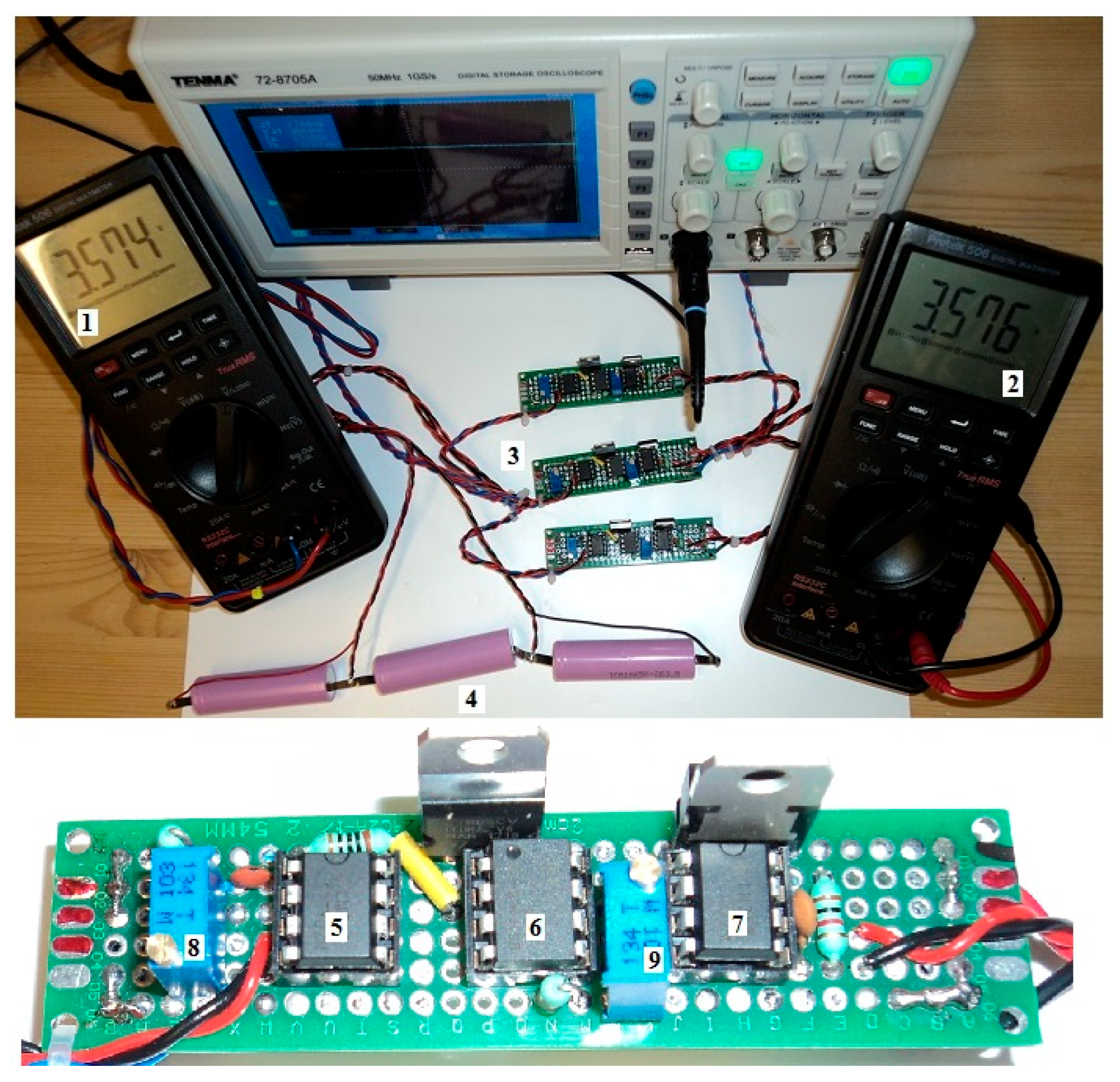
4. Experimental Set-Up

Three experimental boards, shown in Figure 9, have been built and experimentally tested. All elements used in the experimental setup, calculated according to the presented design procedure, are given in Table 2.
Figure 10 shows three oscillograms with input (1) and output (2) DC voltages. The first one presents the input and output DC voltage which are equal. The same result is obtained using two voltmeters in Figure 9, which have equal readings after precise adjustments. Figure 10 also shows the initial transient and the expected propagation delay of about 8 μs, which is a fast-enough response for the designed circuit. On the last oscillogram, the delay is 350 μs due to included first-order RC filters on the input and output.
Figure 11 shows expected voltage ripple on the primary side of the operational amplifier output (probe 1) and operational amplifier feedback (probe 2). Although such ripples with amplitude 100–150 mV can be assumed as acceptable for the destined circuit, they can be minimised with the increasing of the capacitor C1 (Figure 1) in the range of 470 pF–1 nF.
Experimental verification of the system linearity is shown in Figure 12. The two plots of the input and output voltages align perfectly in the range 2–4.2 V with an acceptable error. Respectively, the LED current is also linear. The conducted measurements are shown in Table 3. The relative error is calculated from experimental data using the following equation:
V o u t V b c e l l V b c e l l × 100 %
As the experimental result shows, the error is acceptable for the entire voltage range. The investigated circuit has the potential for even better precision to be achieved. Improved results can be expected under certain environmental laboratory conditions, with standardised laboratory equipment and improved PCB design.

5. Conclusions

The results of the presented work can be summarised as follows:
  • The investigated type of linear optocouplers based on PIN diodes are suitable for galvanic isolated voltage measurement circuits for BMS on the position as shown in Figure 1. The presented circuit (Figure 1, Figure 2) is stable within the entire voltage range of the tested Lithium-ion battery cells with complicit galvanic isolation. Following the requirements given, in Table 1, a robust system with better safety level for automotive and stationary applications can be built. Such a system can be used during the research and development stage of a project or as a permanent solution.
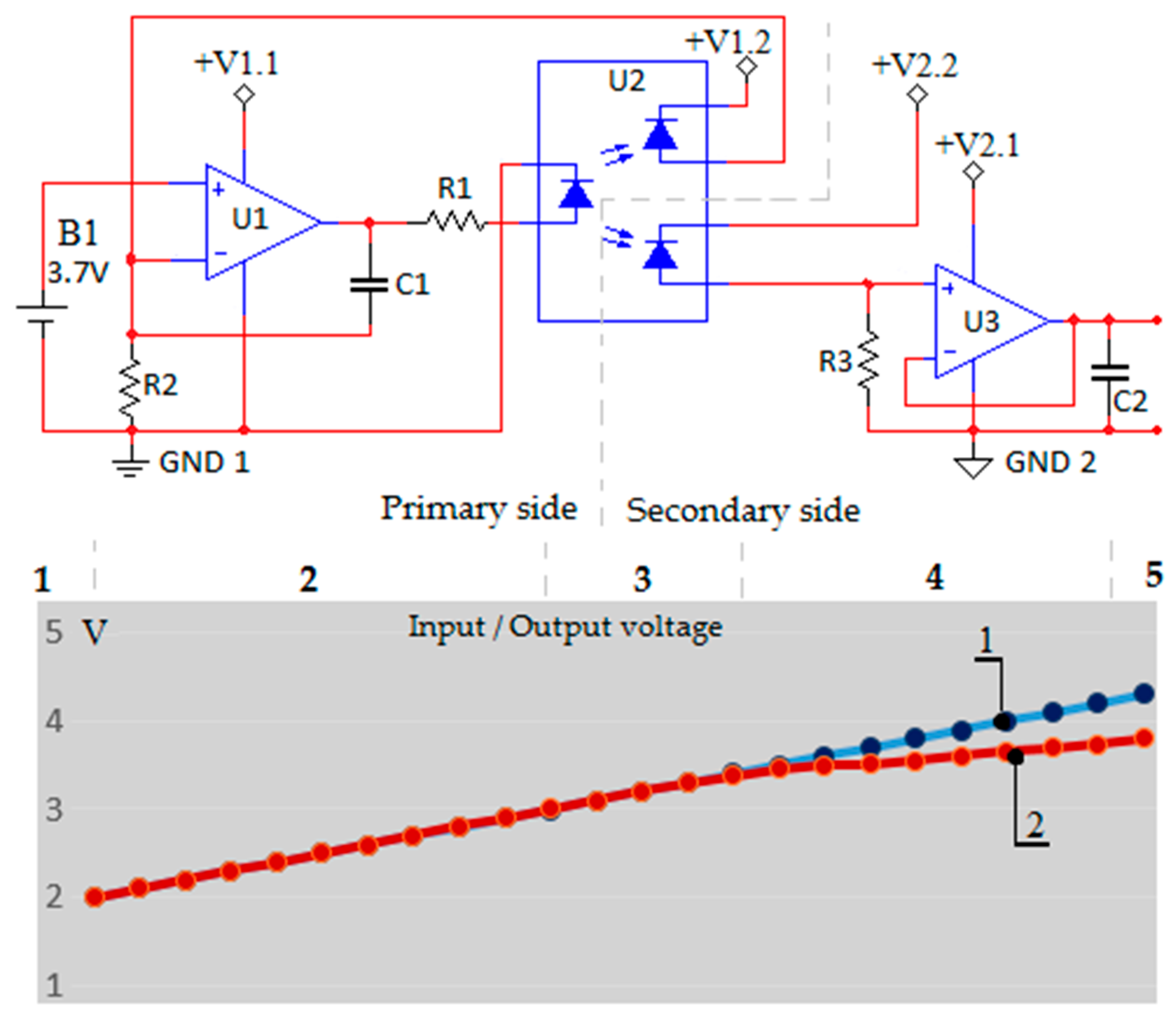
  • The problem with the input/output voltage mismatch can be solved using precise design procedure. A good precision is achieved with digitising the graphical data as Figure 4, Figure 5, Figure 6 and Figure 7 show, respectively transformed to equations Equations (1)–(6), Equations (9)–(11), Equations (12)–(14), and Equations (16)–(21). This approach helps the calculation process to be automated using MATLAB scripts. Additionally, experiments have shown that the power supply voltage of the operational amplifiers on the primary and secondary side have to be 1.5–2 V bigger than the maximum input voltage (4.2 V), i.e., 6–6.5 V, to avoid saturation.
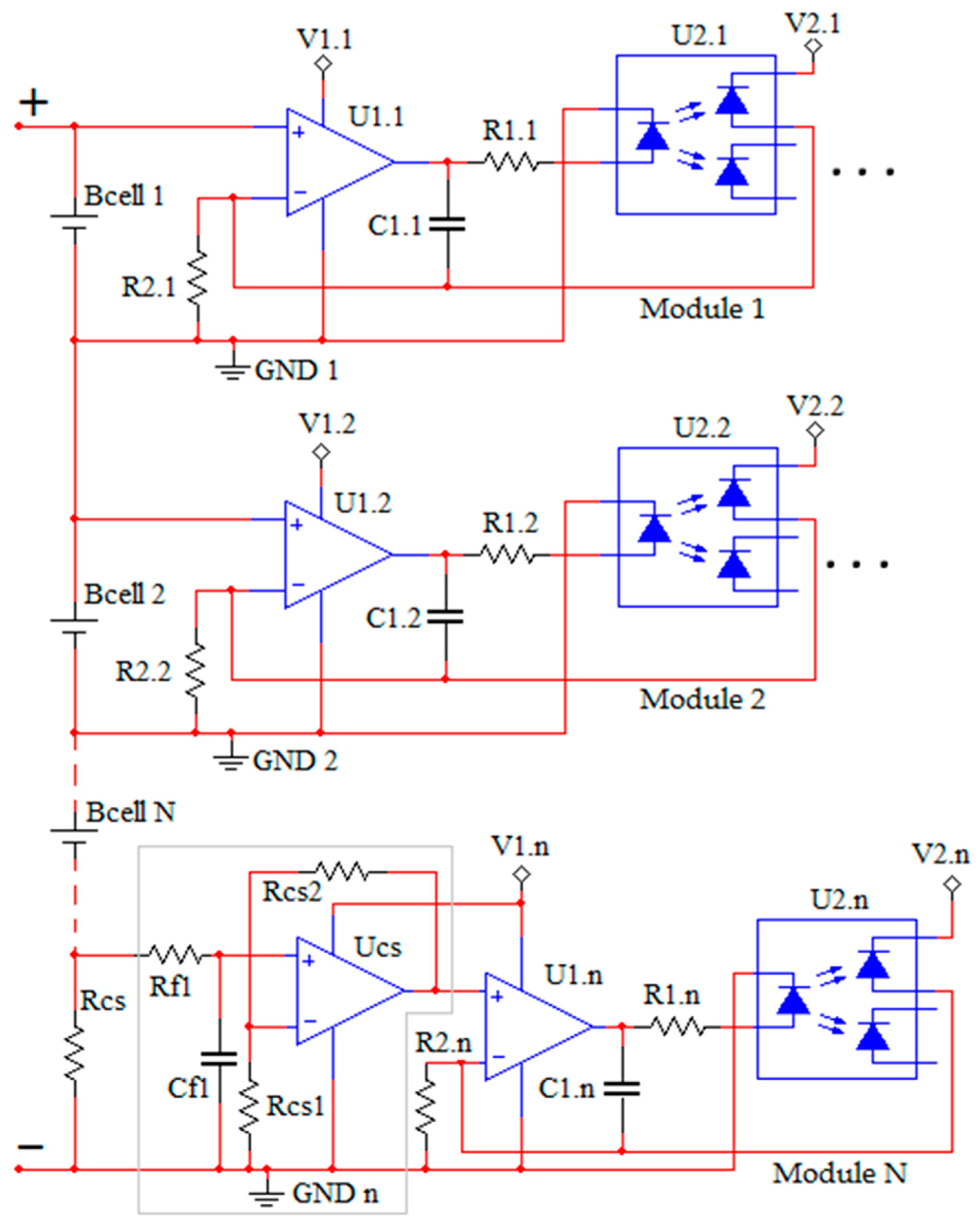
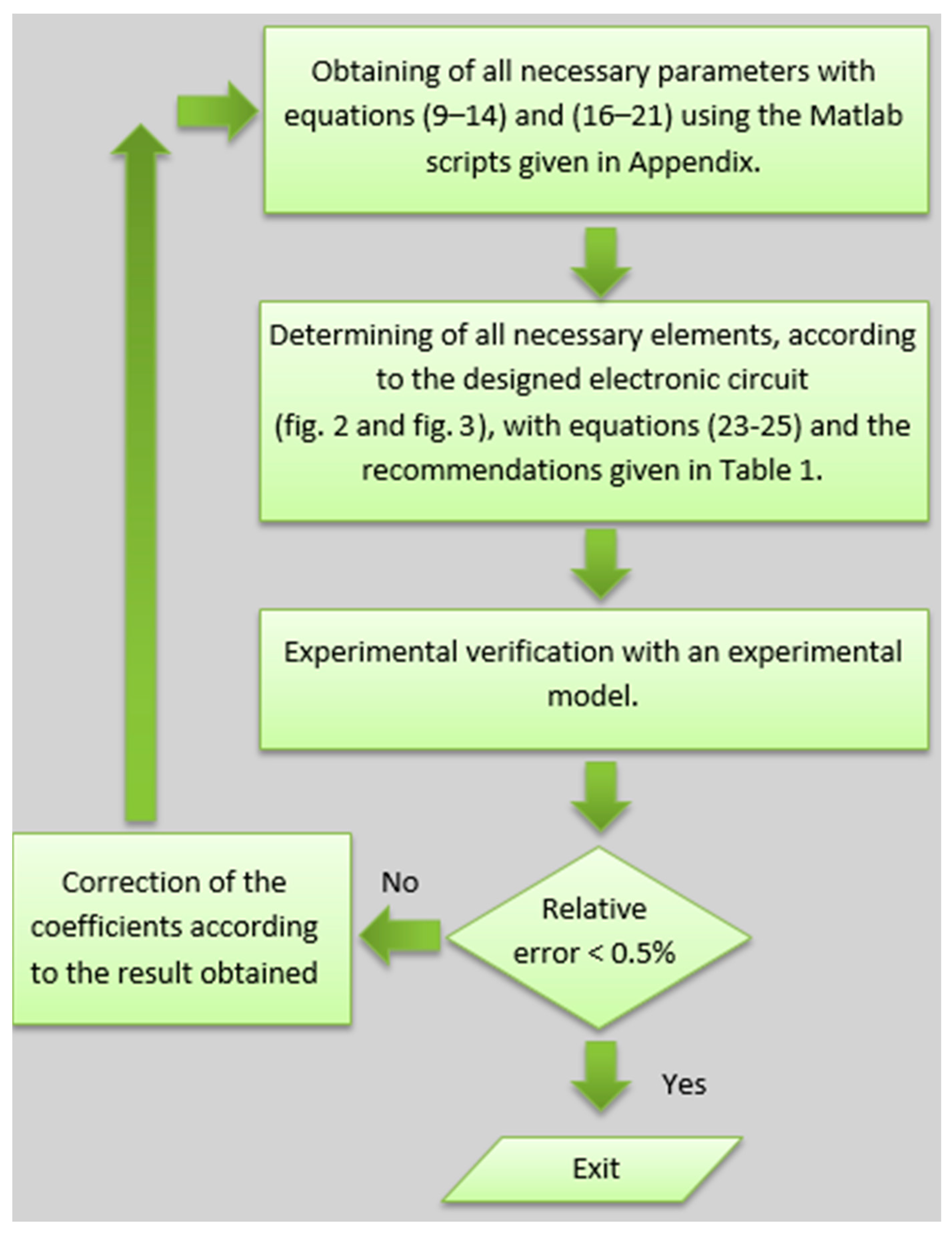
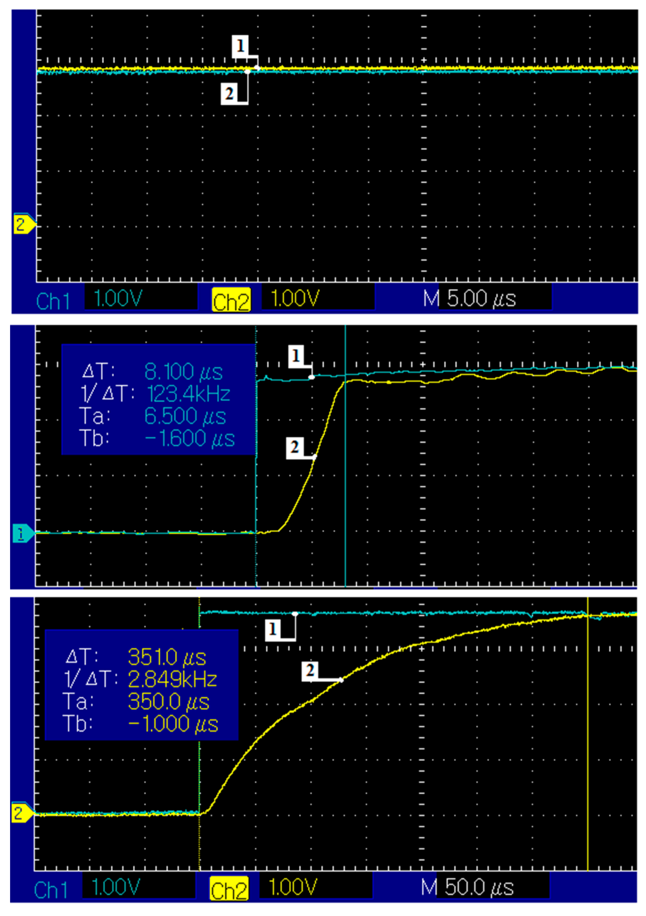
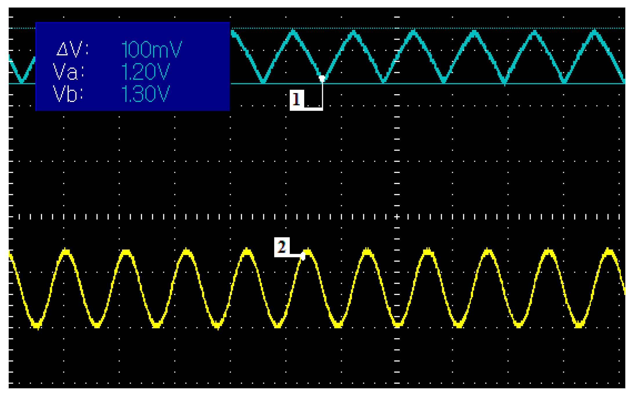
  • The suggested design procedure, derived from the general manufacturers’ manuals, can be used for the successful design of systems with Lithium-ion batteries, applicable for stationary and automotive BMS. The design methodology, shown in Figure 8, has been experimentally proofed as Figure 9, Figure 10, Figure 11 and Figure 12 show. The electronic components selection considerations, given in Table 2, can be used as guidance for future design.

Author Contributions

Conceptualization, B.D. and A.C.; Methodology, G.C.; Software, B.D.; Validation, G.C., A.C; Formal Analysis, B.D.; Investigation, B.D.; Resources, A.C.; Writing-Original Draft Preparation, B.D.; Writing-Review & Editing, G.C.; Supervision, A.C.; Project Administration, A.C.; Funding Acquisition, A.C.

Funding

This work is supported by an EPSRC research grant “ELEVATE—ELEctrochemical Vehicle Advanced TEchnology”, EP/M009394/1.

Conflicts of Interest

The authors declare no conflict of interest.

Appendix A

Listing A1. Calculating of the normalized servo gain with polyval function in Matlab.
clear
format short
NK1_0deg =% matrix (12)
[−1.668069E-7, 14.09345E-6,
−46.61038E-5, 76.48176E-4,
−65.22701E-3, 27.78539E-2,
62.03658E-2];
If = 10;% LED current IF (mA)
polyval (NK1_0deg, If)% ans = 1.1059
Listing A2. Calculating of the transfer gain K3 on 0 degree in Matlab.
clear
format short
If = 10;% LED current IF (mA)
1.0077 * If^−0.0022% Equation (16)
−0.0022 * log(If) + 1.0077% Equation (19)
% ans = 1.0026

References

  1. Affanni, A.A.; Bellini, G.; Franceschini, P.; Guglielmi, C.; Tassoni, C. Battery Choice and Management for New-Generation Electric Vehicles. IEEE Trans. Ind. Electron. 2005, 52, 1343–1349. [Google Scholar] [CrossRef] [Green Version]
  2. Azidin, F.A.; Hannan, M.A.; Mohamed, A. An Energy Management of Light Electric Vehicle. Int. J. Smart Grid Clean Energy 2013, 2, 271–276. [Google Scholar] [CrossRef]
  3. Chatzakis, J.; Kalaitzakis, K.; Voulgaris, N.S.; Manias, S.N. Designing a New Generalized Battery Management System. IEEE Trans. Ind. Electron. 2003, 50, 990–999. [Google Scholar] [CrossRef]
  4. Chen, C.; Man, K.L.; Ting, T.O.; Lei, C.U.; Krilavičius, T.; Jeong, T.; Seon, J.; Guan, S.; Wong, P.W.H. Design and Realization of a Smart Battery Management System. In Proceedings of the International Multi Conference of Engineering and Computer Scientist, Hong Kong, China, 14–16 March 2012; Volume II. [Google Scholar]
  5. Chunyan, X.; Yan, J.; Weichong, Z.; Tao, X. Battery Management System Design and Implementation of Intelligent Emergency Light Based on the Technology of Loose Capacitance and FSM. Int. J. Smart Home 2015, 9, 83–94. [Google Scholar] [CrossRef]
  6. Kavalchuk, I.; Nguyen, H.; Pham, T.; Stojcevski, A. Methodology of Intelligent Energy Management System Simulation for Electric Vehicle Applications with Asynchronous Logic Controller. In Proceedings of the 7th International Conference on Intelligent Systems, Modelling and Simulation, Bangkok, Thailand, 25–27 January 2016. [Google Scholar]
  7. Kim, E.; Lee, J.; Shin, K. Real-Time Battery Thermal Management for Electric Vehicles. In Proceedings of the ICCPS’14, Berlin, Germany, 14–17 April 2014. [Google Scholar]
  8. Kim, G.; Gonder, J.; Lustbader, J.; Pesaran, A. Thermal Management of Batteries in Advanced Vehicles Using Phase-Change Materials. World Electr. Veh. J. 2008, 2, 134–147. [Google Scholar] [CrossRef] [Green Version]
  9. De Hoog, J.; Jaguemont, J.; Abdel-Monem, M.; Van Den Bossche, P.; Van Mierlo, J.; Omar, N. Combining an Electrothermal and Impedance Aging Model to Investigate Thermal Degradation Caused by Fast Charging. Energies 2018, 11, 804. [Google Scholar] [CrossRef]
  10. Liu, P.; Zhang, X. The Design of Smart Battery Management Systems. J. Comput. 2011, 6, 2484–2490. [Google Scholar] [CrossRef]
  11. Vitols, K. Design of an Embedded Battery Management System with Passive Balancing. In Proceedings of the 6th European Embedded Design in Education and Research IEEE, Milan, Italy, 11–12 September 2014. [Google Scholar]
  12. Pitorac, C. An Inside Look in The Electrical Structure of the Battery Management System Topic Number: Renewable Power Sources, Power Systems and Energy Conversion. Int. J. Tech. Res. Appl. 2015, 3, 8–12. [Google Scholar]
  13. Zhang, L.; Peng, H.; Ning, Z.; Mu, Z.; Sun, C. Comparative Research on RC Equivalent Circuit Models for Lithium-Ion Batteries of Electric Vehicles. Appl. Sci. 2017, 7, 1002. [Google Scholar] [CrossRef]
  14. Lelie, M.; Braun, T.; Knips, M.; Nordmann, H.; Ringbeck, F.; Zappen, H.; Sauer, D. Battery Management System Hardware Concepts: An Overview. Appl. Sci. 2018, 8, 534. [Google Scholar] [CrossRef]
  15. Khan, M.R.; Swierczynski, M.; Kær, S. Towards an Ultimate Battery Thermal Management System: A Review. Batteries 2017, 3, 9. [Google Scholar] [CrossRef]
  16. Xing, Y.; Ma, E.; Tsui, K.; Pecht, M. Battery Management Systems in Electric and Hybrid Vehicles. Energies 2011, 4, 1840–1857. [Google Scholar] [CrossRef]
  17. Mathew, M.; Janhunen, S.; Rashid, M.; Long, F.; Fowler, M. Comparative Analysis of Lithium-Ion Battery Resistance Estimation Techniques for Battery Management Systems. Energies 2018, 11, 1490. [Google Scholar] [CrossRef]
  18. Xu, J.; Wang, J.; Li, S.; Cao, B. A Method to Simultaneously Detect the Current Sensor Fault and Estimate the State of Energy for Batteries in Electric Vehicles. Sensors 2016, 16, 1328. [Google Scholar] [CrossRef] [PubMed]
  19. Lin, C.; Mu, H.; Zhao, L.; Cao, W. A New Data-Stream-Mining-Based Battery Equalization Method. Energies 2015, 8, 6543–6565. [Google Scholar] [CrossRef] [Green Version]
  20. Yuan, S.; Wu, H.; Yin, C. State of Charge Estimation Using the Extended Kalman Filter for Battery Management Systems Based on the ARX Battery Model. Energies 2013, 6, 444–470. [Google Scholar] [CrossRef]
  21. Shang, Y.; Zhang, Q.; Cui, N.; Zhang, C. A Cell-to-Cell Equalizer Based on Three-Resonant-State Switched-Capacitor Converters for Series-Connected Battery Strings. Energies 2017, 10, 206. [Google Scholar] [CrossRef]
  22. Dimitrov, B.; Cruden, A.; Krishna, M.; Sharkh, S.; Elkhateb, A. Analysis Design and Experimental Verification of a Primary Side Current Sensing Flyback Converter Used in a Battery Management System. J. Electron. 2018, 7, 43. [Google Scholar] [CrossRef]
  23. Chen, C.; Hu, Y.; Luo, W.; Wang, C.; Juan, C. A High Voltage Analog Multiplexer with Digital Calibration for Battery Management Systems. In Proceedings of the IEEE International Conference on IC Design Technology, Austin, TX, USA, 30 May–1 June 2012. [Google Scholar]
  24. Chon, S.; Beall, J. Intelligent Battery Management and Charging for Electric Vehicles, Texas Instruments Manuscript. Available online: https://www.ti.com/lit/wp/spry304a/spry304a.pdf (accessed on 21 April 2019).
  25. Datasheet ISL94202. Series Charge/Discharge Path 3-to-8 Cell Li-Ion Battery Pack Monitor. Available online: https://www.renesas.com/eu/en/doc/datasheet/isl94202.pdf (accessed on 20 July 2019).
  26. Datasheet LTC6802-2. Multicell Addressable Battery Stack Monitor, Linear Technology. Available online: https://www.analog.com/media/en/technical-documentation/data-sheets/68022fa.pdf (accessed on 20 July 2019).
  27. Datasheet BQ769X0. 3-Series to 15-Series Cell Battery Monitor Family for Li-ion and Phosphate Applications. Available online: http://www.ti.com/lit/ds/symlink/bq76940.pdf (accessed on 20 July 2019).
  28. Datasheet MC33771B. Battery Cell Controller IC. Available online: https://www.nxp.com/docs/en/data-sheet/MC33771B_SDS.pdf (accessed on 21 April 2019).
  29. Datasheet MAX11068. 12-Channel, High-Voltage Sensor, Smart Data-Acquisition Interface, Industry’s First Li+ Battery-Management IC for Hybrid Electric Vehicle Applications, Maxim Integrated. Available online: https://www.maximintegrated.com/en/products/power/battery-management/MAX11068.html (accessed on 20 July 2019).
  30. Andrea, D. Battery Management Systems for Large Lithium-Ion Battery Packs; Artech House: London, UK, 2010; ISBN 978-1-60807-104-3. [Google Scholar]
  31. Daowd, M.; Antoine, M.; Omar, N.; Bossche, P.; Mierlo, J. Single Switched Capacitor Battery Balancing System Enhancements. Energies 2013, 6, 2149–2174. [Google Scholar] [CrossRef] [Green Version]
  32. Lin, J. Development of a New Battery Management System with an Independent Balance Module for Electrical Motorcycles. Energies 2017, 10, 1289. [Google Scholar] [CrossRef]
  33. Brandl, M.; Gall, H.; Wenger, M.; Lorentz, V.; Giegerich, M.; Baronti, F.; Fantechi, G.; Fanucci, L.; Roncella, R.; Saletti, R.; et al. Batteries and battery management systems for electric vehicles. In Proceedings of the 2012 Design, Automation Test in Europe Conference Exhibition, Dresden, Germany, 12–16 March 2012. [Google Scholar]
  34. Vishay Semiconductors. Linear Optocouplers Manufacturer. Available online: https://www.vishay.com (accessed on 21 April 2019).
  35. Vishay Semiconductors. Application Note 50, Designing Linear Amplifiers Using the IL300 Optocoupler. Available online: https://www.vishay.com/docs/83708/appnote50.pdf (accessed on 20 July 2019).
  36. Vishay Semiconductors. IL300 Datasheet, Linear Optocoupler, High Gain Stability, Wide Bandwidth. Available online: http://www.vishay.com/docs/83622/il300.pdf (accessed on 20 July 2019).
  37. Broadcom Inc. Linear Optocouplers Manufacturer. Available online: https://www.broadcom.com/ (accessed on 20 July 2019).
  38. Broadcom Inc. HCNR200 Datasheet, High-Linearity Analog Optocouplers. Available online: https://www.broadcom.com/products/optocouplers/industrial-plastic/specific-function/high-linearity-analog/hcnr201 (accessed on 20 July 2019).
  39. Avago. HCNR201 Datasheet, Application Note 1357, Overview of High Performance Analog Optocouplers. Available online: https://wenku.baidu.com/view/1ddfb7e2b8f67c1cfad6b83a.html?re=view (accessed on 20 July 2019).
  40. IXYS. Linear Optocouplers Manufacturer. Available online: https://www.ixys.com/ (accessed on 20 July 2019).
  41. IXYS. LOC110 Datasheet, Single Linear Optocoupler. Available online: http://www.ixysic.com/home/pdfs.nsf/www/LOC110.pdf/$file/LOC110.pdf (accessed on 20 July 2019).
  42. IXYS. LOC111 Datasheet, Single Linear Optocoupler. Available online: http://www.ixysic.com/home/pdfs.nsf/www/LOC111.pdf/$file/LOC111.pdf (accessed on 20 July 2019).
  43. IXYS. LOC111 Datasheet, Single Linear Optocoupler. Available online: http://www.ixysic.com/home/pdfs.nsf/www/LOC112.pdf/$file/LOC112.pdf (accessed on 20 July 2019).
  44. IXYS. LOC117 Datasheet, Single Linear Optocoupler. Available online: http://www.ixysic.com/home/pdfs.nsf/www/LOC117.pdf/$file/LOC117.pdf (accessed on 20 July 2019).
  45. IXYS. LOC210 Datasheet, Dual Linear Optocoupler. Available online: http://www.ixysic.com/home/pdfs.nsf/www/LOC210.pdf/$file/LOC210.pdf (accessed on 20 July 2019).
  46. IXYS. LOC211 Datasheet, Dual Linear Optocoupler. Available online: http://www.ixysic.com/home/pdfs.nsf/www/LOC211.pdf/$file/LOC211.pdf (accessed on 20 July 2019).
  47. Jang, W. Op Amp Applications Handbook; Analog Devices, Inc.: Norwood, MA, USA, 2005; ISBN 0-7506-7844-5. [Google Scholar]
  48. Zumbahlen, H. Basic Linear Design; Analog Devices, Inc.: Norwood, MA, USA, 2007; ISBN 0-916550-28-1. [Google Scholar]
  49. Power, X.P. ITX DC-DC Converters. Available online: https://www.xppower.com (accessed on 20 July 2019).
  50. Datasheet, L.M. 358, Texas Instrument. Available online: http://www.ti.com/lit/ds/symlink/lm158-n.pdf (accessed on 20 July 2019).
Figure 1. A battery pack with BMS (battery management system) and suggested circuit for galvanic isolation.
Wevj 10 00059 g001
Figure 2. Structure of the linear optocoupler, connected as unipolar photoconductive isolation amplifier. (1—battery cell; 2—input operational amplifier; 3—linear optocoupler which provides galvanic isolation; 4—secondary side voltage followers; 5—input to the BMS ASIC (Figure 1) or microcontroller.) Accompanying graph is an example of the experimental result showing voltage mismatch: plot 1—input voltage; plot 2—output voltage.
Wevj 10 00059 g002
Figure 3. Schematic of the battery management system, power supply with galvanic disconnection on the primary and secondary side.
Wevj 10 00059 g003
Figure 4. Functional dependency between the photocurrent IP1 (µA) and the LED current IF (mA). (Plot 1, 2 and 3: 0 °C; 25 °C and 75 °C respectively).
Wevj 10 00059 g004
Figure 5. Functional dependency between K1 and IF (Plot 1, 2 and 3: 0 °C; 25 °C and 75 °C respectively).
Wevj 10 00059 g005
Figure 6. Dependency between the normalized servo gain and the LED current IF(mA). (Plot 1, 2 and 3: 0 °C; 25 °C and 75 °C respectively).
Wevj 10 00059 g006
Figure 7. Dependency between the transfer gain and the LED current IF(mA). (Plot 1, 2 and 3: 0 °C; 25 °C and 75 °C respectively).
Wevj 10 00059 g007
Figure 8. A procedure for compiling and correction of the Equations (9)–(14) and (16)–(21).
Wevj 10 00059 g008
Figure 9. Experimental prototype of the designed input voltage measurement system with galvanic isolation. 1—input voltage from a battery cell; 2—output voltage; 3—three experimental PCBs; 4—three battery cells connected in series. 5—primary side operational amplifier; 6—linear optocoupler; 7—secondary side operational optocoupler; 8, 9—primary and secondary side potentiometers for adjustments.
Wevj 10 00059 g009
Figure 10. Oscillogram of the input (probe 1) and output (probe 2) voltages. Steady-state and transient conditions.
Wevj 10 00059 g010
Figure 11. Ripples at the operational amplifier output (probe 1) and feedback circuit (probe 2).
Wevj 10 00059 g011
Figure 12. Experimental results—input voltage (1) from the battery cell and output voltage (2) to the ASIC (microcontroller), and photocurrent through the primary side LED.
Wevj 10 00059 g012
Table 1. Functionality of the electronic elements used and recommendations for their selection.
Element (Reference Figure 2 and Figure 3)Recommendations for Elements Selection
Primary side operational amplifier U1The design of the primary and secondary operational amplifier circuits has been done according to the well-established literature for analog circuits [47,48] and is not presented in detail here.
As Figure 2 shows, the non-inverting input is directly connected to the Lithium-ion cell. For this application, an input divider would not be necessary as the cell voltage matches the input voltage op-amp range. However, a first-order R-C filter can be used the input voltage ripples during the charging process to be filtered at the input.
Resistor R1It limits the LED current I L E D through U2 primary side LED.
Resistor R2It adjusts the servo feedback connection from the primary side photodiode, respectively the output I L E D current.
Resistor R3It adjusts the secondary side photocurrent, respectively the voltage on the voltage follower which must be equal to the V b c e l l .
Effectively the entire circuit precision depends on resistors R1, R2 and R3 tolerances, and therefore a 0.1% tolerance is required.
Linear optocoupler U2The key building block of this design. All of the above-given optocouplers [34,35,36,37,38,39,40,41,42,43,44,45,46] have similar structure and parameters, which make them applicable for this design.
Secondary side operational amplifier U3As amplification in this design is not necessary, i.e., the input-output transfer ratio must be 1:1, a circuit with a voltage follower has been chosen, in order for the necessary current to be supplied to the next stage (ASIC or microcontroller). The requirements for the secondary side operational amplifier are the same as these to the primary side. The primary and the secondary side operational amplifiers must be separated not to share the same ground (different ICs). The same requirement is set for the amplifiers between the different channels (Figure 3) i.e., they must operate with separate ground lines.
Capacitor C1Compensation capacitor for system stability. According to the manufacturers’ recommendations, it can be in the range 20–100 pF, 1%, ceramic SMD or through-hole capacitor.
Capacitor C2Optional output filtering capacitor. Depending on the input ripples during the charging process, it can be used within R-C first-order analog filter.
Current sense operational amplifier UcsA non-inverting amplifier with resistors R c s 1 , R c s 2 and the first-order filter R f 1 , C f 1 , connected to the current sense resistor are used. Due to its simplicity, it is not an object of this research. At this position other types of current sensing circuits, for example, Hall current sensing circuits can also be used successfully.
Power supply voltages.The two power supply voltages on the primary and secondary side must be isolated. The auxiliary power supplies are usually Printed Circuit Board (PCB) DC-DC isolated converters [49] which can be used for low power electronic circuits.
Table 2. Electronic elements used for the experimental model.
Element According to Figure 2 and Figure 3ValueNotice
R1100 Ω,This value limits the LED current in the range 10–20 mA, according to the manufacturers’ requirements for the linear range of operation and the input voltage tolerance.
R2, R350 kΩ,It has to be calculated from the presented design procedure according to the linear optocoupler parameters. In the experimental models, as Figure 9 shows, two multi-turns potentiometers by 50 kΩ have been used only for research purposes, but eventually, constant value resistors must be applied. Their precise values must be calculated according to Equations (24) and (25).
C120 pF, 16 V,A ceramic capacitor, selected at 20 pF according to the manufacturers’ recommendations has been used for the first experiment. Eventually, its value has been increased for better stability.
C21–4.7 nF, 16 VCeramic capacitors in this range have been used for all conducted experiments. If necessary, their value can be reduced in order to reduce the time constant of the circuit.
U1, U3LM 358A general application operation optocoupler would be suitable for this purpose i.e., other types of low budget operational amplifiers are also acceptable. Here, an optocoupler designed specifically for unidirectional power supply has been chosen [50]. Their supply voltages (V1.1. and V2.1., Figure 2) have been set at 6 V to ensure that saturation at 4.2 V is avoided.
U2IL300Other types of linear optocouplers, as previously shown, have also been tested with the same results. The primary and secondary supply voltages for the photodiodes (V1.2. and V2.2., Figure 2) have been set at 5 V with two linear regulators (Figure 9).
The presented equations: Equations (1)–(6), Equations (9)–(11), Equations (12)–(14), Equations (16)–(21) are the product of this research and have been derived with trend analysis for this linear optocoupler. For other optocouplers, the same approach can be used and different coefficients must be specified. However, the structure and the order of magnitude in the equations would be the same, as the optocouplers characteristics are similar.
Table 3. Experimental verification.
Input Voltage V b c e l l LED Current (mA)Output Voltage V o u t V o u t V b c e l l (mV)Relative Error (%)
29.182.00110.05
2.210.092.20330.136
2.411.012.40990.375
2.611.912.61100.384
2.812.832.80990.321
313.743.01100.33
3.214.663.20770.219
3.415.573.40880.235
3.616.493.61100.278
3.817.413.81100.263
418.324.01100.25
4.219.254.21100.238

