Influence of Nanoscaled Surface Modification on the Reaction of Al/Ni Multilayers


1
Institute of Micro- and Nanotechnologies, Technische Universität Ilmenau, 98693 Ilmenau, Germany
2
Facultad de Ciencias, Universidad de Cádiz, 11510 Puerto Real, Spain
3
Institute of Research on Electron Microscopy and Materials, Universidad de Cádiz, 11002 Cádiz, Spain
4
Physics Department, Pontificia Universidad Católica del Perú, San Miguel, 15088 Lima, Peru
*
Author to whom correspondence should be addressed.
Technologies 2017, 5(4), 79; https://doi.org/10.3390/technologies5040079
Submission received: 9 November 2017
/
Revised: 3 December 2017
/
Accepted: 4 December 2017
/
Published: 7 December 2017
(This article belongs to the Section Innovations in Materials Processing)
Abstract
:Sputtered reactive multilayers applied as a heat source in electronic joining processes are an emerging technology. Their use promises low-stress assembly of components while improving thermal contact and reducing thermal resistance. Nanostructured surface modifications can significantly enhance adhesion and reliability of joints between different materials. This work examines reactive multilayer of nickel and aluminum, directly sputtered on nanostructured black silicon surfaces and compares their phase transformation with reference samples deposited on pristine silicon surface. The investigation of the quenched self-propagating reaction reveals a clear influence of the nanostructured surface on the prolongation of the phase transition. Rapid thermal annealing tests result in the formation of Al1.1Ni0.9 phase. The nanostructured interface seems to hinder the full transformation of the parent material. The surface modification improves the adhesion of the formed alloy on silicon surfaces and can possibly increase the reliability of joints based on reactive aluminum/nickel multilayer. The use of black silicon, a nanostructured surface modification, is thus a promising approach to realize reliable multi-material joints in complex systems.
1. Introduction
Today’s electronic systems must provide increased performance whilst reducing size at the same time. This pushes the development of effective and cost-efficient methods of heat removal [1]. Overall thermal challenges encompass hot spot thermal management on packaging level and heat spreading from chips to heat sinks [2]. This entails enhanced requirements on thermal interface materials [3]. The direct mount of chips on heat sinks, strongly driven by packaging requirements of LED chips, enters the field of integrated circuit and microelectromechanical systems (MEMS) packaging. However, the assembly of complex dies with numerous contacts and fine pitch creates high demands and the huge mismatch of thermal expansion between silicon and heat sink must be compensated in order to minimize stress.
One solution for stress minimization is the use of local heat exposure during the bond process [4]. Self-propagating exothermic reactions of multilayer films can be used to generate a local heat source and melt a solder between silicon chips and a board or heat sink. The reaction is driven by a reduction in atomic binding energy. The mechanism is observed when multilayer films of bimetal layers with a single layer thickness between 10 nm and 150 nm—such as Ni/Si, Al/Ti, Al/Ni, or Al/Pd—are ignited with an energy pulse, e.g., an electric spark or a laser pulse.
Several works dwell on the use of such reactive multilayers (RML) for chip joining. One approach uses aluminum nickel nanofoils in combination with indium solder. A thermal interface with improved performance in comparison with a polymeric-based interface is created at room temperature. Due to a very restricted heating zone, the thermal stress is minimized and a tight bond is achieved [5]. The direct deposition of reactive layers on components expands the material variety and allows improved stress control. Sputtered Ti/Si and Al/Pd multilayers form bond interfaces using Sn solder for the assembly of silicon MEMS at room temperature [6]. These integrated RML allow the direct and hermetic bond between two silicon chips and between silicon and ceramic, and glass and metal as well [7]. Al/Ni integrated RML, directly deposited on low temperature cofired ceramics (LTCC) can be used for the joining of copper heat sinks. The higher roughness of the ceramic substrate leads to a better adhesion in comparison with pristine wafer surfaces [8]. Al/Ni RML stand out through a very fast exothermic propagation, easy preparation, and easy ignition. However, stress control is an ongoing topic using these materials in order to avoid cracks and voids which reduces thermal performance [9]. Besides thermal performance increase, improved mechanical compliance is an ongoing target in the development of thermal interface materials (TIMs). A metallic interlayer can be used to increase the strength, because the type of interlayer influences the fracture origin [10]. Another approach to stress reduction is the use of nanostructured interfaces. Nanothermal interfaces can reach very low thermal resistance, undercutting values of 1 W/m−1K−1 [11]. An enhancement of the bonding strength can be achieved by surface modifications of silicon in the nanoscale. Surface enlargement and additional form fit affect adhesive bond strength and ductility of the interface [12,13]. Plasma etching of the silicon surface generates nanostructures by self-masking, the so-called black silicon [14]. The cost-effective process can be easily applied on any silicon surface in plasma processes used for mesa-structure etching of chips. If this surface modification entails a stress reduction in combination with RML chip assembly, the chip would be optimally prepared and additional process steps such as sputtering of intermediate layers can be omitted. With this motivation, the present work aims to provide the first insight into the interplay between surface morphology and reaction behavior of Al/Ni RML. A comparison between pristine silicon wafer surface and black silicon modified silicon wafer surface, sputtered with aluminum/nickel as parent multilayer, is the base of the discussion—focusing on parent multilayer growth, reactive multilayer thickness, and their influences on phase forming and reaction propagation. On this base, a scenario for possible applications of RML on black silicon as nanothermal interface for chip mounting is outlined.
2. Materials and Methods
Black silicon is formed as a consequence of self-organized micromasking in fluorine based reactive ion etch processes of silicon wafers [14]. The geometry of the needles depends on the etch process [15]. In this work, nanostructure etching is performed in an Oxford RIE reactor with a pressure of 100 mTorr, working at a power of 100 W and 20 °C with helium backing, using a gas flow of 84 sccm SF6, and 66 sccm O2. P-doped (111) silicon wafers are used as the substrate. The process was maintained for 30 min, resulting in needles of approximately 1.0 µm of length. A pristine, flat wafer without nanostructures is used for comparison purpose. On both substrate types, the nanostructured silicon wafer and the flat ones, aluminum/nickel RML are directly applied. The layer consists of alternating nanoscaled single layers of pure aluminum and nickel which were deposited by magnetron sputtering. The bilayer thickness amounts to 50 nm. The process was carried out using a cluster system (CS400 by ARDENNE) with a sputtering power of 200 W and a working pressure of 5 × 10⁻³ mbar with 80 sccm argon flow and without substrate heating. The obtained deposition rate was 0.32 nm/s for aluminum and 0.26 nm/s for nickel. The total thickness of the multilayer sequence varies between 250 nm and 5 µm. The experimental design is summarized in Table 1.
The prepared wafers are mechanically carved along the substrate’s main crystallographic directions using a diamond tip and broken in samples with an edge length between 1 and 2 cm. One piece of each wafer was stored for reference, one was ignited by electric spark, and three pieces were annealed at different temperatures. The layer morphology on the nanostructures was investigated by SEM (Field-Effect ZEISS Gemini SEM 500 working at 1.5 kV and working distance of 8 mm, Carl Zeiss Microscopy GmbH, Jena, Germany) and TEM (TECNAI S20 working at 200 kV, FEI, Eindhoven, Netherlands). SEM micrographs were obtained by positioning the broken pieces of the samples, without further preparation, in a planar or a transversal disposition regarding to the electron beam. TEM preparation consisted of scratching the nanostructured and coated surface of the samples with a surgical blade, in order to separate the needles from the silicon substrate. The separated needles were deposited on holey carbon grids without further preparation for TEM measurements. The images of SEM and TEM analysis are depicted in Figure 1. Self-propagating reactions were initiated on one sample of each wafer. An electric spark was formed between a platinum electrode and the coated surface, applying a voltage of 50 V and a maximum current of 50 mA with a lab power supply. Fifty ignition points were generated, and their dimensions were investigated with a light microscope in order to assess the influenced region dependent on multilayer thickness on an adequate confidence level. The influenced region can be identified by a color change with a light microscope. The affected area of the nanostructured samples and the 5 µm thick flat sample were investigated with a light microscope (Nikon Eclipse LV100POL, Nikon GmbH, Essen, Germany) and the radius of the affected spots was measured with the microscopes image processing software (NIS Elements Imaging Software 4.30.00, Nikon). The discolored area is enclosed with a circle, defined on three points on the circumference, the software calculates the affected radius raff and the values are summarized in an Excel sheet. The box plots in Figure 2a display median and quantiles of the respective value distribution on nanostructured samples. The morphology of the affected zone was investigated by SEM. Fused areas were subsequently colored in purple to achieve a better visibility. Selected pictures are depicted in Figure 2b–e.
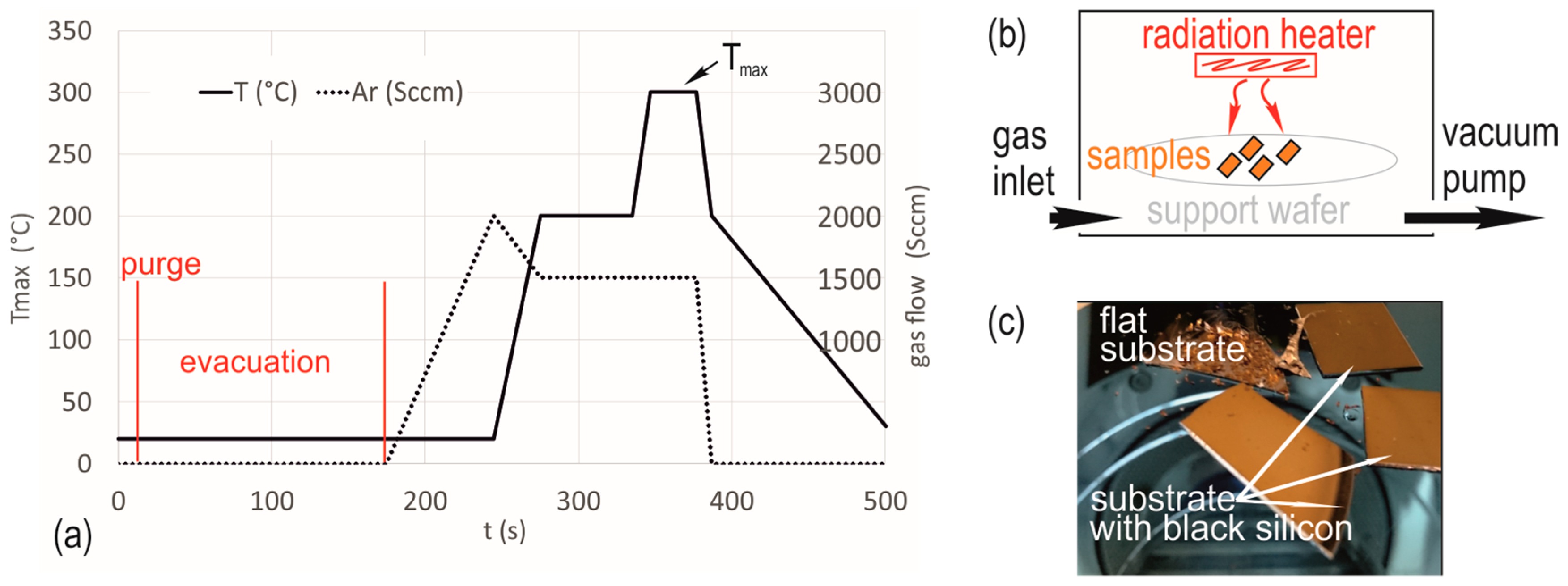
Furthermore, samples of each wafer were annealed in a rapid thermal furnace (Jet First, Joint Industrial Processor for Electronics) under argon atmosphere (RTA). The maximum temperature Tmax was varied between 350 °C and 550 °C. Figure 3a illustrates temperature treatment and gas flow regime. Figure 3b gives a schematic of the reactor setup. Treated and untreated samples were investigated with a laser scanning microscope (LSM, Olympus OLS4100, Olympus Europa SE & Co., KG, Hamburg, Germany), selected surface pictures and a height profile are compared in Figure 4. The treated samples were investigated with XRD (Bruker D5000 diffractometer with Göbel mirror, working in Bragg-Brentano mode at a speed of 0.1 s per step, using sampling steps of 0.04° without sample rotation, Bruker AXS Analytical X-Ray Systems GmbH, Karlsruhe, Germany) to identify formed phase and grade of phase formation. Diffractograms were recorded over the 20° < 2θ < 100° range. Phase identification was performed by analyzing the positions and intensities of the peaks observed in the diffractograms and comparing them with data bases patterns. Extracts between 20° and 65° are depicted in Figure 5. Energy dispersive X-ray spectroscopy (EDX) is carried out at 20 kV acceleration voltage (EDAX detector with super ultra-thin window of 30 mm² area, nitrogen cooled, AMETEK GmbH, Weiterstadt, Germany) in order to determine the chemical composition.
3. Results
3.1. Parent Multilayer Morphology on Nanostructures
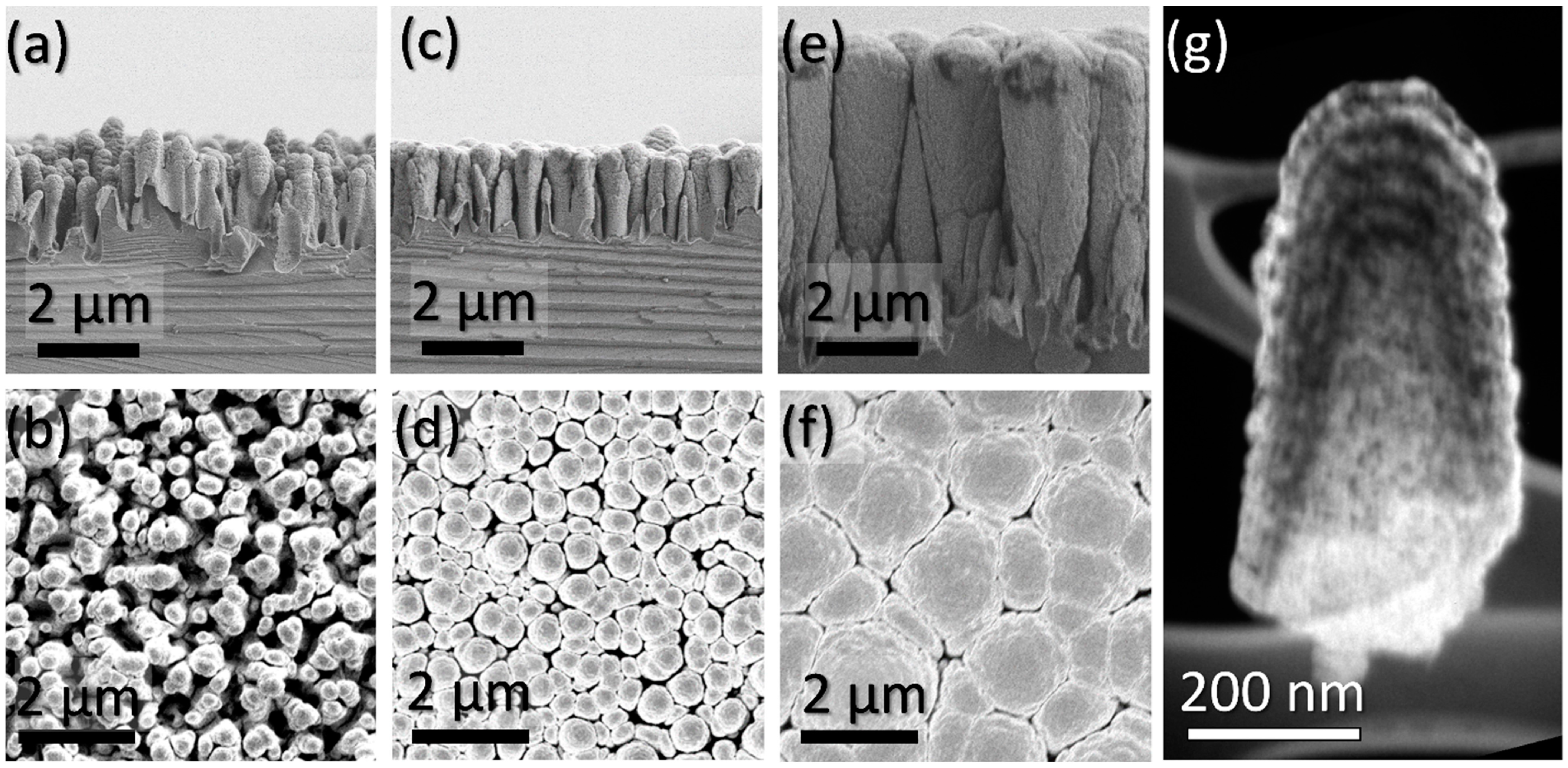
The parent bilayer layer consists of alternating sequences of fcc Ni and fcc Al, identified by comparison of the XRD diffractograms with PDF 03-065-2865 and PDF 03-065-2869. EDX analysis reveals a composition of 50 at % Ni: 50 at % Al with a deviation of 3%. The cross sections in Figure 1a,c,e illustrate that the edge coverage of the sputtered layers on black silicon is not uniform. A progressive growth of larger clusters at the structure’s top occurs at the expense of smaller clusters. With increasing thickness, the gaps between single nanostructures are filled from the top of the substrate. While single structures covered with a 500-nm-thick multilayer still are separated, some touch at the top when the layer is 1 µm thick. The black silicon structures covered with a 5-µm-thick layer have direct contact on top, visible in the top view Figure 1b,d,f. However, the cross sections indicate that hollows are present at deeper levels. The TEM image in Figure 1g reveals that the deposition rate at the nanostructure’s foot is much lower than on top, resulting in a steady decrease of the bilayer thickness. At a depth of approx. 500 nm from the top of the structure, the bilayer thickness is only ¼ of the one on the structure top. In all probability, the intermixed layer formed during sputtering and pure metal layers reaches similar thickness at the structure foot, resulting in disruption of the crystal structure, grain boundary structure, and lattice structure in this region.
3.2. Spark Ignition
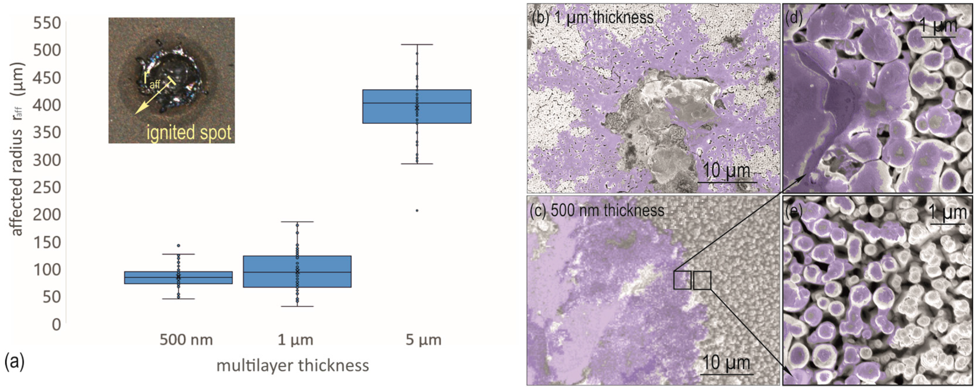
Molten ares are visible on all samples around the ignition point. This molten zone is surrounded with a ring, which can be recognized by a color change under the ligth microscope. The border of this region marks the end of the affected material and is used to asses the affected zone by spark ignition. The box plot of the affected zones radius raff, measured on black silicon for different Al/Ni multilayer thickness, is depicted in Figure 2a. The values follow a Gaussian distribution. The dependency of the median values of raff on layer thickness can be approximated by a quadratic polynom with high accuracy. Median values correspond to 84 µm for 500 nm Al/Ni multilayer thickness, 92 µm for 1 µm and 391 µm for 5 µm. The comparison between raff of the 5-µm-thick flat sample, which amounts to 468 µm, and this of the nanostrutured interface with equal RML thickness shows that black silicon surface modification narrows down the affected zone. Raff is reduced to 80 percent. The shape of the affected area on black silicon is depicted in Figure 2b,c. The influenced zone of 5 µm-thick-layer (not depicted) and 500 nm thick layers are characterized by a round contour. The transition ring area between molten material and unaffected structures has a width of 100 µm for 5-µm-thick layers. In the case of 500-nm-thick layers, it is restricted to approximately 10 µm. Details of this transition area are depicted in Figure 2d,e. While the structures in the near vicinity still show closed molten links to the spark area, those next to them are characterized by a changed morphology, but not linked with adjacent ones. Ignited regions on samples with 1-µm-thick Al/Ni multilayers are characterized by a dendrite shape of the molten areas. The reaction propagates along paths were the tips of the nanostructures have contact and peter out. The affected area identified by light microscope has mostly circular, and in some cases eliptical contours.
3.3. Rapid Thermal Annealing
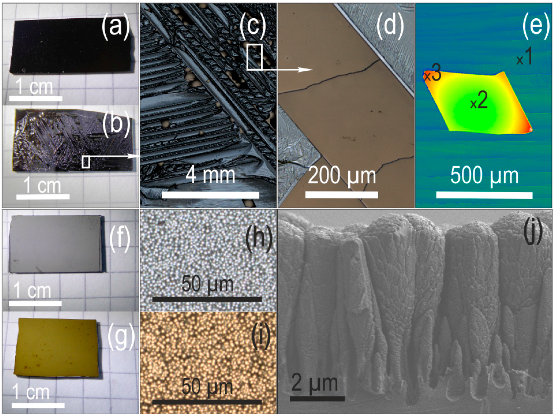
The RTA process uses heat radiation to initiate the phase transformation, which is here driven by solid diffusion. Layers on flat silicon surfaces (compare Figure 4a) flake during the treatment, independently from thickness and maximum temperature. An example is depicted in Figure 4b–e. A remarkable orientation of chipped traces is visible in Figure 4b. The peel-off seems to follow the single-crystal structure of the silicon substrate. Trapezoidal flakes are formed as depicted in Figure 4c. These exhibit strong tensile stress, which can be concluded from the strong bend visible in Figure 4e. Layers on black silicon showed excellent adhesion without exception. Photographs of samples with 1 µm coating before and after treatment at 450 °C are depicted in Figure 4f,g. Surface images captured with LSM are depicted in Figure 4h,i. The phase transformation can optically be identified by the color change. Neither the LSM top view, Figure 4i, nor the cross-sectional SEM image, Figure 4j, exhibit signs of molten material.
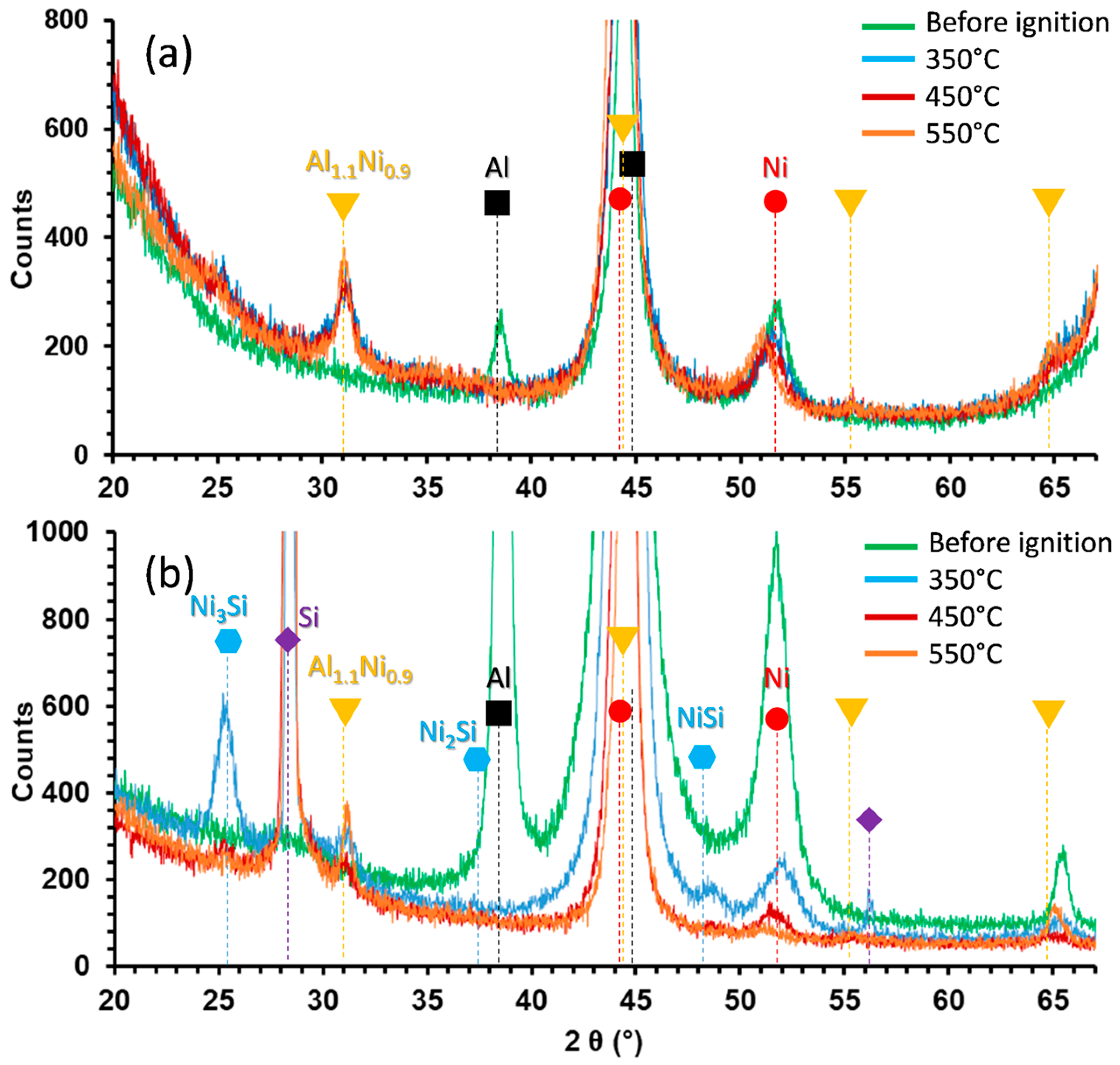
XRD difractograms are depicted in Figure 5. The parent materials exist in form of fcc Al (PTC 03-065-2869) and fcc Ni (PTC 03-065-2865) before RTA. (111) Al peak at 2θ = 38.471° and (200) Ni peak at 2θ = 51.847° are clearly evident. Between 44° < 2θ < 45°, both parent materials and possible formed Ai/Ni phases as well have peaks, for that reason these cannot contribute to analysis. After annealing, the (111) Al peaks disappear, and the AlNi phase peaks arise around 2θ = 31.2° and 55.5°. Further peaks AlNi are present at 65.023° and 73.869°. The significant Al (111) and Ni (200) peaks are evaluated to assess the parent material presence. Diffractograms of Al1.1Ni0.9 and Al0.42Ni0.58 phase are very similar; therefore, they cannot be identified explicitly on the base of the measured XRD data. Consulting the EDX results and considering the fact that fcc Ni is still present after RTA, it can be assumed that Al1.1Ni0.9 (PDF 044-1187) is formed in this process, independently from surface modification and layer thickness. Peaks of fcc Ni were found on all black silicon samples in Figure 5a. Its intensity decreases slightly with increasing Tmax. This effect can be explained by emerging portions of the Ni-rich Al0.42Ni0.58 phase, which is formed at higher temperatures. Equally, it decreases on flat wafers with Tmax and here it disappears totally at Tmax = 550 °C, compared with Figure 5b. Strong Si peaks appear in this measurement due to regions where the reactive layer is peeled off. The samples annealed at 350 °C show additional peaks, indicating the presence of Ni/Si phases. The intensity of the peaks related to Ni/Si phases disappear with increasing Tmax.
The intensities of (111) Al peak, (200) Ni peak, and (100) Al1.1Ni0.9 are used as markers to estimate the relation of present parent material and Al1.1Ni0.9 phase portions in the mixed crystal. The relative intensity IrelM of the respective metal is calculated using Equation (1). The index M is representative of the respective metal: Al = aluminum, Ni = nickel and AlNi = Al1.1Ni0.9 phase. The intensities IAl, INi, and INiAl are extracted from fitted curves of the respective measurement.
4. Discussion
4.1. Self-Propagation of the Reaction Front
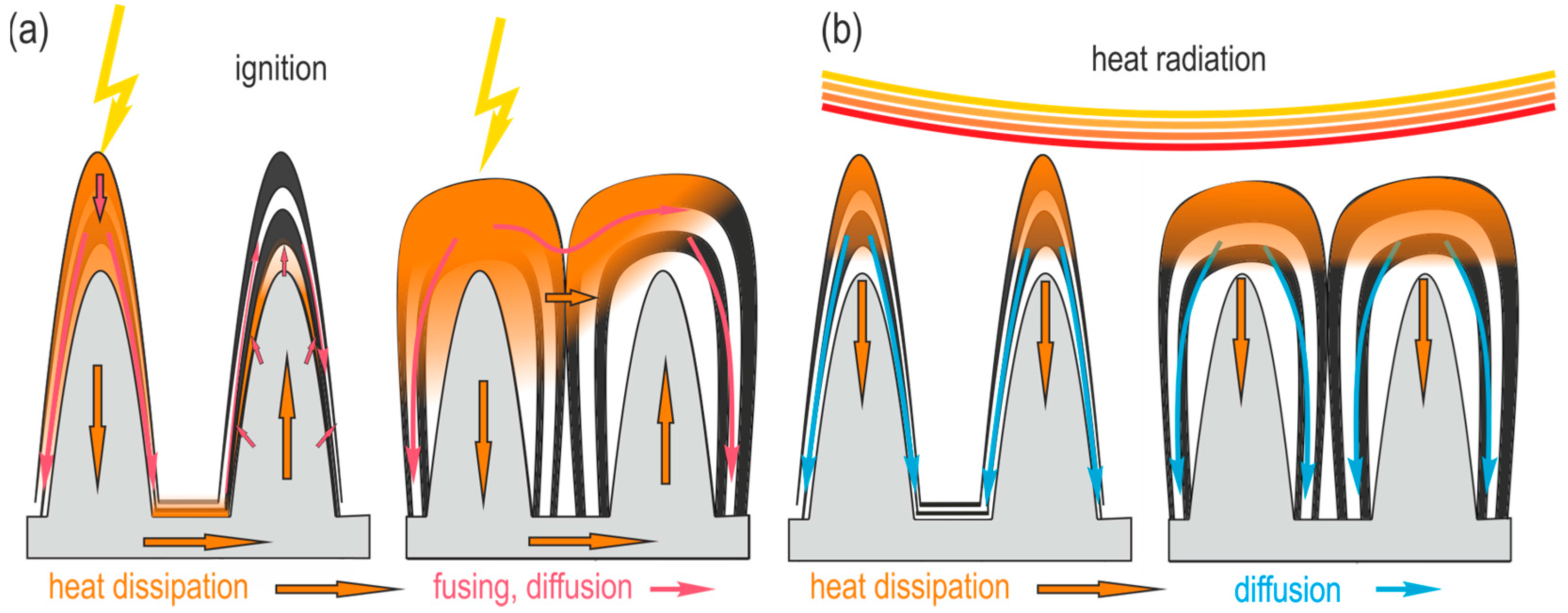
Spark ignition creates a local hot spot, which heats a small region and initiates a chain reaction. The propagation depends on amount of heat release and the level of heat losses to the environment. It peters out when the balance of dissipated heat and reaction enthalpy, which is released during the exothermic process, fall below the necessary activation energy. Figure 2 reveals molten areas around the ignition points. Color changes identified by light microscope around the molten region indicate a transition zone of the quenched reaction. The influenced area increases with layer thickness and has a round shape as pointed out in Figure 2a. An irregularity is observed on the samples with 1 µm RML thickness. In this case, fused tips peter out astrally, which is visible in the SEM picture in Figure 2b. The self-propagating reaction spreads preferably along the tips of nanostructures with close contact. Figure 8a illustrates the propagation process. The diffusion in thin layers must follow the nanostructure contour, which enlarges the necessary diffusion path. The temperature at the ignition point is high enough that the aluminum can melt and solid–liquid diffusion of Ni can occur. The fused areas are visible in Figure 2c–d. In parallel, high thermal conductivity of the silicon substrate causes a rapid heat distribution. This can initiate additional solid–solid diffusion if the transformation temperature is reached. This is assumed to be the reason for the formation of the transition zone. Figure 2e depicts this transition zone for 500-nm-thick layer, which spreads over a length of 10 µm, approximately. It seems that some separated nanostructures are molten form the bottom. The zone observed on 5-µm-thick layers spans a dimension of 100 µm. This arises from the circumstance that the larger reactive volume generates a higher heat release whilst heat dissipation conditions remain similar.
When the RML becomes thicker, the reaction wave starts to propagate along contact points at the nanostructure tip. When the black silicon is covered with 1 µm thick RML layer, some structures come into contact (compare Figure 1d). The propagation along these contact points is the reason for the irregular shape of the molten area occurring at this thickness (Figure 2b). RML with a thickness of 5 µm have a dense contact at the structure tip. This enables fusing along the layer top, enhancing propagation. However, compared to RML deposited on flat surface, the affected radius is smaller indicating that black silicon surface modification hinders the propagation.
The influence of grain boundary defects and the very low thickness of the RML at the foot of black silicon cannot clearly be judged. Some indications can be found in the literature: experiments reveal that stacking faults and defects cause a decrease of the chain reaction efficiency if the bilayer thickness fall below 20 nm [16]. A reduced cross section of the RML can hinder the propagation of the reaction front and can be used to slow down the velocity [17,18]. Molecular dynamic investigations suggest that amorphous aluminum present at grain boundaries promotes the reaction [19]. The observation in the present experiments suggest that the black silicon surface modification hinders the reaction. Detailed investigations on an atomic scale are needed to understand the complex process of combustion waves propagating along curved structures with dimensions in the nanoscale.
4.2. Rapid Thermal Annealing Tests
The dominant phase transformation mechanism during RTA is solid-state reaction, no molten areas were observed on the samples. The heat radiation initiates the phase transformation at the nanostructure tips and the transformation propagates perpendicular to the substrate plane, as illustrated in Figure 8b. Intermetallic phases around the stoichiometric AlNi composition are formed. The Al1.1Ni0.9 phase contains 42–47 at % Ni [20]. Diffusion studies on Al-Ni-interfaces have shown that the formation of intermetallic phases starts with Al-rich ones [21] as a consequence of the lower melting point of the material. The sputtered parent RML contains stoichiometric composition of Al and Ni. In RTA treated RML deposited on black silicon, fcc Ni still is present even at Tmax of 550 °C. The decreasing fcc Ni content with temperature is attributed to emerging Ni-rich intermetallic phase, which requires higher temperatures [22]. The effect occurs similarly on flat samples, but here the excessive fcc Ni already disappears at lower temperatures. A part of the excessive Ni forms a material bound with the silicon substrate on flat surfaces (see Figure 5b). However, SiNi phases could not be found on the nanostructured samples (Figure 5a). This might be due to the penetration depth of the X-ray measurement, which might hinder the detection of occurring similar phases at the nanostructured interface on the backside of the well adhered layers on these samples. A second possibility is that the nanostructure hinders the phase formation.
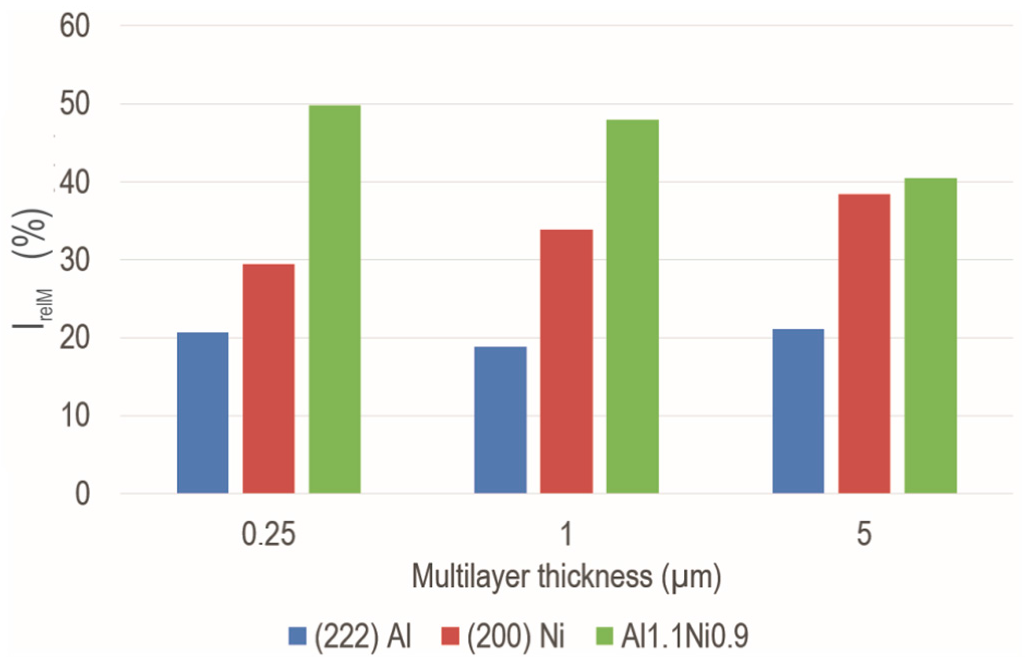
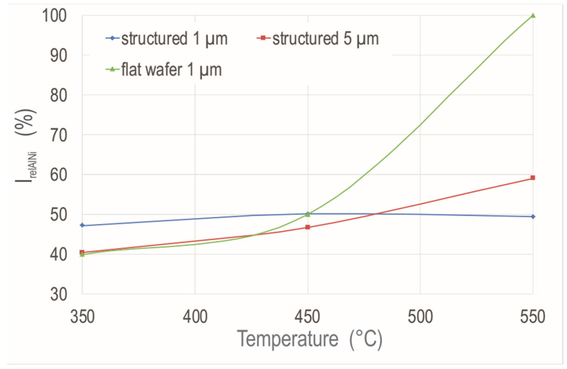
The comparison of the relative peak intensity IrelM in Figure 6 demonstrates that the annealing temperature of 350 °C is too low to achieve a complete transformation of RML on black silicon. The remaining fcc Ni content increases with increasing RML thickness and fcc Al content remains stable at the same time. This indicates that a complete transformation of the parent materials is not achieved and Al-rich phase is formed preferably. The incompleteness of the transformation increases with layer thickness, indicating that the annealing temperature of 350 °C is too low to initiate an exothermic chain reaction, because otherwise the released energy would foster a transformation. An increase of the temperature up to 550 °C (Figure 7) also fails to lead to a complete transformation. In comparison to this, 1-µm-thick RML can be completely transformed at Tmax 550 °C if they are applied on flat silicon. It can therefore be concluded that the nanostructured surface hinders the transformation.
5. Conclusions
Reactive Al/Ni multilayers were deposited on nanostructured black silicon and pristine flat silicon wafer for comparison purpose. The black silicon interface disturbs the morphology of the parent AlNi multilayer, in particular at the foot of the nanostructure. In comparison with the flat surface, black silicon hinders the self-propagating reaction initiated by electric spark. The solid-state reaction initiated by rapid thermal annealing could not fully transform the parent materials on black silicon, whilst it was achieved for flat surfaces at a maximum temperature 550 °C. The reaction is hindered by the nanostructure as well. This behavior can help to control the reaction dynamics and it can be used to control the reaction propagation when the RML is used for chip assembly on heat sinks. The presence of almost stoichiometric AlNi phases leads to the conclusion, that high temperatures have been achieved. Thus, the use of RML on black silicon as local heat source for soldering processes with restricted heat-affected zone is possible.
The significantly enhanced adhesion of the RML on black silicon in comparison with the pristine wafer surface promises an additional improvement of the reliability of the thermal interface. Further studies must investigate stress, considering different chip assembly scenarios.
Since nanostructure influences the microstructure of the parent material, reaction propagation, and interface morphology, precise studies of single effects are necessary. As an optimum approach to understand this complex process, a combination of molecular dynamic simulations and experimental work will be the focus of following studies.
Acknowledgments
The authors acknowledge for the support from the Alexander von Humboldt Foundation, through the “Humboldt Research Fellowship for Postdoctoral Researchers Program” (Ref. 3.3-1 1S8421-ES-HFST-P). A special thank goes to Jens Müller for supervising this exchange. Furthermore, the authors would express deep thankfulness to Peter Schaaf who enabled the sound cooperation among all staff of the material science department of IMN MacroNano® and the authors as base for this study.
Author Contributions
Heike Bartsch designed the experiments, performed the experiments, interpreted the results and wrote the paper. José Manuel Mánuel performed SEM and TEM studies, carried out XRD measurements and analyzed the respective data. Rolf Grieseler conceived the experiment and provided his experience of reactive multilayer processing and analysis. He supported the methodology concept and discussion section.
Conflicts of Interest
The authors declare no conflict of interest.
References
- Grace O’Malley. Highlights from the iNEMI Thermal Management Technology Roadmap, Advancing in Manufacturing Technology. 2014. Available online: http://thor.inemi.org/webdownload/2014/Eurotherm_061914.pdf (accessed on 4 December 2017).
- Yeh, L.-T. Thermal Management/Roadmap and Energy Efficiency for Telecommunications Equipment. J. Comput. Intel. Electron. Syst. 2015, 4, 1–9. [Google Scholar] [CrossRef]
- Mahajan, R.; Chiu, C.-P.; Prasher, R.S. Thermal Interface Materials: A Brief Review of Design Characteristics and Materials. Electron. Cool. 2004, 10, 10–18. [Google Scholar]
- Welker, T.; Geiling, T.; Bartsch, H.; Müller, J. Design and Fabrication of Transparent and Gas-Tight Optical Windows in Low-Temperature Co-Fired Ceramics. Int. J. Appl. Ceram. Technol. 2013, 10, 405–412. [Google Scholar] [CrossRef]
- Subramanian, J.; Rodgers, P.; Newson, J.; Rude, T.R.; He, Z.; Besnoin, E.; Weihs, T.; Eveloy, V.; Pecht, M. Room Temperature Soldering of Microelectronic Components for Enhanced Performance. In Proceedings of the IEEE International Conference on Thermal, Mechanical and Multiphysics Simulation and Experience in Microelectronics and Microsystems, Berlin, Germany, 18–20 April 2006; pp. 681–686. [Google Scholar]
- Bräuer, J.; Besser, J.; Wiemer, M.; Gessner, T. A novel technique for MEMS packaging: Reactive bonding with integrated material systems. Sens. Actuators A Phys. 2012, 188, 212–219. [Google Scholar] [CrossRef]
- Bräuer, J.; Gessner, T. A hermetic and room-temperature wafer bonding technique based on integrated reactive multilayer systems. J. Micromech. Microeng. 2014, 24, 115002. [Google Scholar] [CrossRef]
- Grieseler, R.; Welker, T.; Müller, J.; Schaaf, P. Bonding of low temperature co-fired ceramics to copper and to ceramic blocks by reactive aluminum/nickel multilayers. Phys. Status Solidi A 2012, 209, 512–518. [Google Scholar] [CrossRef]
- Miyake, S.; Kanetsuki, S.; Morino, K.; Kuroishi, J.; Namazu, T. Thermal property measurement of solder joints fabricated by self-propagating exothermic reaction in Al/Ni multilayer film. Jpn. J. Appl. Phys. 2015, 54, 06FP15. [Google Scholar] [CrossRef]
- Namazu, T.; Ohtani, K.; Inoue, S.; Miyake, S. Influences of Exothermic Reactive Layer and Metal Interlayer on Fracture Behavior of Reactively Bonded Solder Joints. J. Eng. Mater. Technol. 2015, 137, 031011. [Google Scholar] [CrossRef]
- Bar-Cohen, A.; Matin, K.; Narumanchi, S. Nanothermal Interface Materials: Technology Review and Recent Results. J. Electron. Packag. 2015, 137, 040803. [Google Scholar] [CrossRef]
- Feng, B.; Cao, J.; Wang, Y.; Feng, J. Enhanced Adhesive Bonding Based on Surface Modification with Silicon Nanowire Arrays. ECS J. Solid State Sci. Technol. 2015, 5, P41–P46. [Google Scholar] [CrossRef]
- Fischer, M.; Bartsch, H.; Pawlowski, B.; Gade, R.; Barth, S.; Mach, M.; Stubenrauch, M.; Hoffmann, M.; Müller, J. Silicon on Ceramics—A New Integration Concept for Silicon Devices to LTCC. J. Microelectron. Electron. Packag. 2009, 1, 1–5. [Google Scholar] [CrossRef]
- Jansen, H.V.; de Boer, M.J.; Unnikrishnan, S.; Louwerse, M.C.; Elwenspoek, M.C. Black silicon method X: A review on high speed and selective plasma etching of silicon with profile control: An in-depth comparison between Bosch and cryostat DRIE processes as a roadmap to next generation equipment. J. Micromech. Microeng. 2009, 19, 033001. [Google Scholar] [CrossRef]
- Pezoldt, J.; Kups, T.; Stubenrauch, M.; Fischer, M. Black luminescent silicon. Phys. Status Solidi C 2011, 8, 1021–1026. [Google Scholar] [CrossRef]
- Theodossiadis, G.D.; Zaeh, M.F. Study of the kinetic and energetic reaction properties of multilayered aluminum–nickel nanofoils. Prod. Eng. Res. Devel. 2017, 11, 245–253. [Google Scholar] [CrossRef]
- Sraj, I.; Vohra, M.; Alawieh, L.; Weihs, T.P.; Knio, O.M. Self-Propagating Reactive Fronts in Compacts of Multilayered Particles. J. Nanomater. 2013, 2013, 1–11. [Google Scholar] [CrossRef]
- Fritz, G.M.; Joress, H.; Weihs, T. Enabling and controlling slow reaction velocities in low-density compacts of multilayer reactive particle. Combust. Flame 2011, 158, 1084–1088. [Google Scholar] [CrossRef]
- Politano, O.; Baras, F.; Mukasyan, A.S.; Vadchenko, S.G.; Rogachev, A.S. Microstructure development during NiAl intermetallic synthesis in reactive Ni-Al nanolayers: Numerical investigations vs. TEM observations. Surf. Coat. Technol. 2013, 215, 485–492. [Google Scholar] [CrossRef]
- Urrutia, A.; Tumminello, S.; Aricó, S.F.; Sommadossi, S. Characterization of Al-Ni intermetallics around 30–60 at % Al for TLPB application. CALPHAD Comput. Coupl. Phase Diagr. Thermochem. 2014, 44, 108–113. [Google Scholar] [CrossRef]
- Tumminello, S.; Sommadossi, S. Growth Kinetics of Intermetallic Phases in Transient Liquid Phase Bonding Process (TLPB) in Al/Ni System. Defect Diffus. Forum 2012, 323–325, 465–470. [Google Scholar] [CrossRef]
- Urrutia, A.; Tumminello, S.; Lamas, D.G.; Sommadossi, S. X-Ray Characterization of Intermetallic Phases in Al/Ni Multilayer System. Proced. Mater. Sci. 2015, 8, 1150–1159. [Google Scholar] [CrossRef]
Figure 1.
SEM micrographs of multilayers with different thickness, grown on black silicon nanostructures: (a,c,e) cross section of multilayers with 500 nm, 1 µm, and 5 µm thickness; (b,d,f) top view on the respective layer; (g) dark field TEM image of a nanostructure tip with 20 nm radius, coated with a 250-nm-thick multilayer.

Figure 2.
Affected zone dependent on layer thickness on nanostructured surface. (a) box plot of the affected radius measured by light microscope as function of layer thickness; (b) false color SEM image of ignition zone; zone is minimal larger and has dendrite shape, form is irregular, fractal distribution of the ignition over nanostructures on top, molten areas are colored; (c) false color SEM image of 500 nm layer. Ignited zone has a round shape, molten area ends abruptly; (d) detail of the border area, molten layers on top are depicted in false color; (e) outermost area of influenced zone, some tips show fused structure (false color).

Figure 3.
Rapid thermal annealing (RTA) process. (a) Temperature profile with gas flow regime, Tmax varies between 350 °C and 550 °C, the heat-up time is 12 s and plateau time 30 s; (b) schematic of RTA set-up; (c) photograph of treated samples on support wafer.
Figure 3.
Rapid thermal annealing (RTA) process. (a) Temperature profile with gas flow regime, Tmax varies between 350 °C and 550 °C, the heat-up time is 12 s and plateau time 30 s; (b) schematic of RTA set-up; (c) photograph of treated samples on support wafer.

Figure 4.
Comparison of RTA test samples before and after treatment at 450 °C. (a–e) flat silicon chip; (a) before treatment; (b) after treatment; (c) LSM image of the surface after treatment; (d) LSM image of a transformed area; (e) height map of an adhered flake. Height level at point 1 = 0 µm, point 2 = 28 µm, point 3 = 50 µm. (f–j) chips with black silicon; (f) chip with 1 µm RML before treatment; (g) after treatment; (h) LSM image of the chip surface, 5 µm RML before and (i) after treatment; (j) cross-sectional SEM image of the transformed RML with 5 µm thickness.

Figure 5.
XRD Theta-2Theta curve of RTA treated samples with 1 µm RML thickens, (a) on black silicon surface; (b) reference on flat wafer. Identification peaks are associated to PDF 03-065-2869 (fm-3m Al), 03-065-2865 (fm-3m Ni), and 00-044-1187 (pm-3m Al1.1Ni0.9).
Figure 5.
XRD Theta-2Theta curve of RTA treated samples with 1 µm RML thickens, (a) on black silicon surface; (b) reference on flat wafer. Identification peaks are associated to PDF 03-065-2869 (fm-3m Al), 03-065-2865 (fm-3m Ni), and 00-044-1187 (pm-3m Al1.1Ni0.9).

Figure 6.
Relation between the intensities of selected peaks as marker for Al, Ni, and Al1.1Ni0.9 content after RTA treatment at 350 °C.
Figure 6.
Relation between the intensities of selected peaks as marker for Al, Ni, and Al1.1Ni0.9 content after RTA treatment at 350 °C.

Figure 7.
Relative intensity IAlNi for total thickness of 1 µm and 5 µm compared with 1-µm-thick layer on flat reference wafer.
Figure 7.
Relative intensity IAlNi for total thickness of 1 µm and 5 µm compared with 1-µm-thick layer on flat reference wafer.

Figure 8.
Schematic illustration of the mass and heat transport for thin and thick multilayers. (a) Spark ignition; (b) rapid thermal annealing.
Figure 8.
Schematic illustration of the mass and heat transport for thin and thick multilayers. (a) Spark ignition; (b) rapid thermal annealing.


Table 1.
Overview on samples and experimental design.
| No. | Substrate | Bilayer Thickness (nm) | Total RML Thickness (nm) | RTA Tmax (°C) | Spark Ignition (V)/(mA) |
|---|---|---|---|---|---|
| 1 | Flat wafer | 50 | 1000 | 350/450/550 | - |
| 2 | Flat wafer | 50 | 5000 | 350/450/550 | 50/50 |
| 3 | Black silicon | 50 | 500 | 350/450/550 | 50/50 |
| 4 | Black silicon | 50 | 1000 | 350/450/550 | 50/50 |
| 5 | Black silicon | 50 | 5000 | 350/450/550 | 50/50 |
© 2017 by the authors. Licensee MDPI, Basel, Switzerland. This article is an open access article distributed under the terms and conditions of the Creative Commons Attribution (CC BY) license (http://creativecommons.org/licenses/by/4.0/).
Share and Cite
MDPI and ACS Style
Bartsch, H.; Mánuel, J.M.; Grieseler, R. Influence of Nanoscaled Surface Modification on the Reaction of Al/Ni Multilayers. Technologies 2017, 5, 79. https://doi.org/10.3390/technologies5040079
AMA Style
Bartsch H, Mánuel JM, Grieseler R. Influence of Nanoscaled Surface Modification on the Reaction of Al/Ni Multilayers. Technologies. 2017; 5(4):79. https://doi.org/10.3390/technologies5040079
Chicago/Turabian StyleBartsch, Heike, José Manuel Mánuel, and Rolf Grieseler. 2017. "Influence of Nanoscaled Surface Modification on the Reaction of Al/Ni Multilayers" Technologies 5, no. 4: 79. https://doi.org/10.3390/technologies5040079
Note that from the first issue of 2016, this journal uses article numbers instead of page numbers. See further details here.