Polarization Beam Splitter Based on Si3N4/SiO2 Horizontal Slot Waveguides for On-Chip High-Power Applications

 ,
,  and
and
Abstract
:1. Introduction
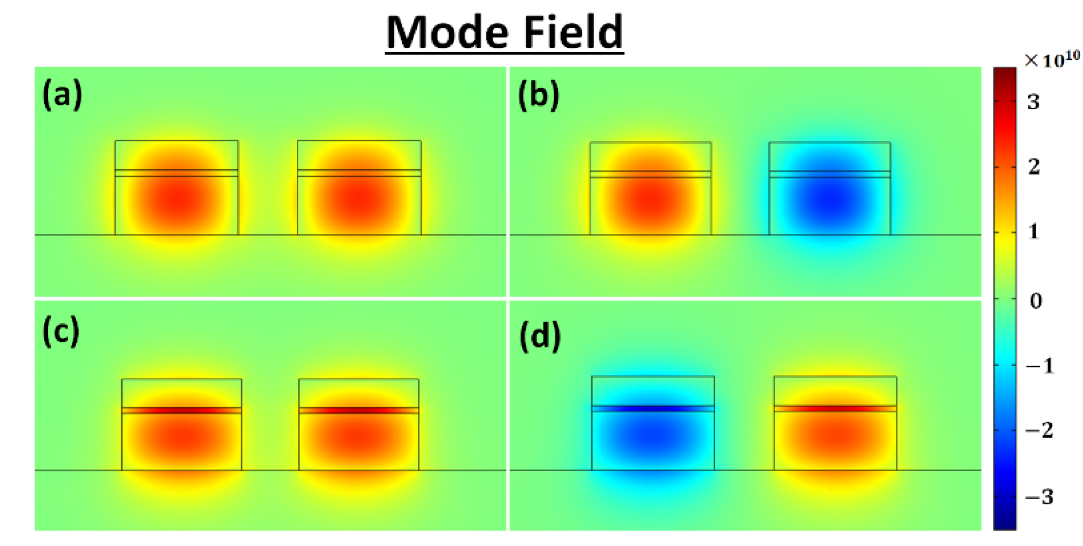
2. Concept
3. Resultant Design of the Polarization Beam Splitter
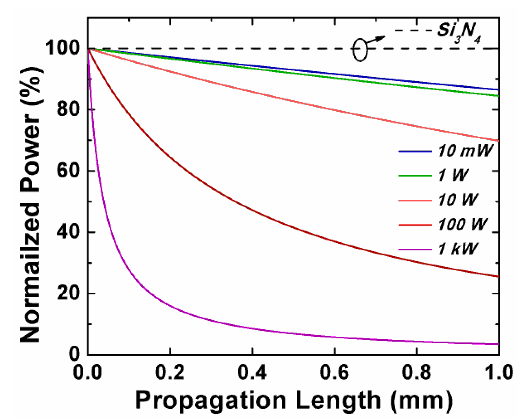
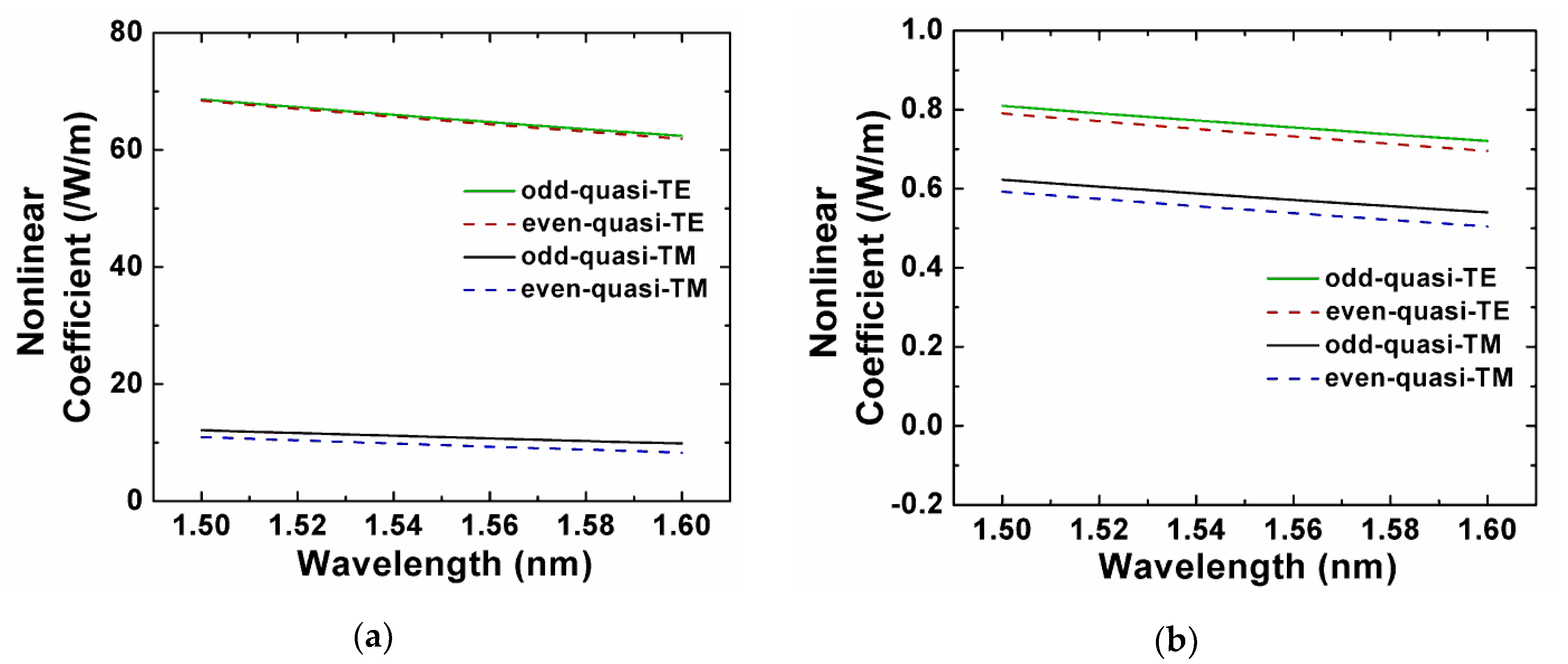
3.1. Material Characteristics
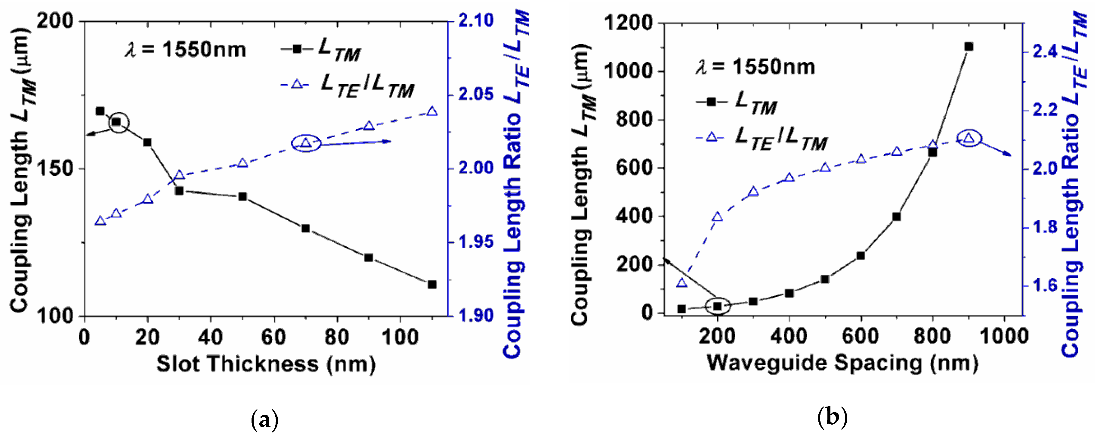
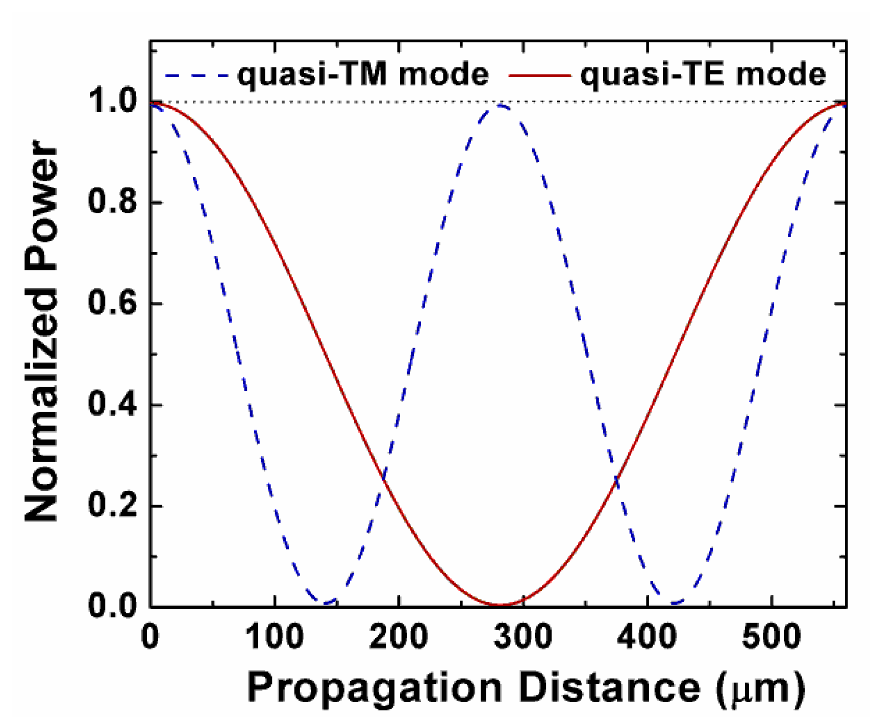
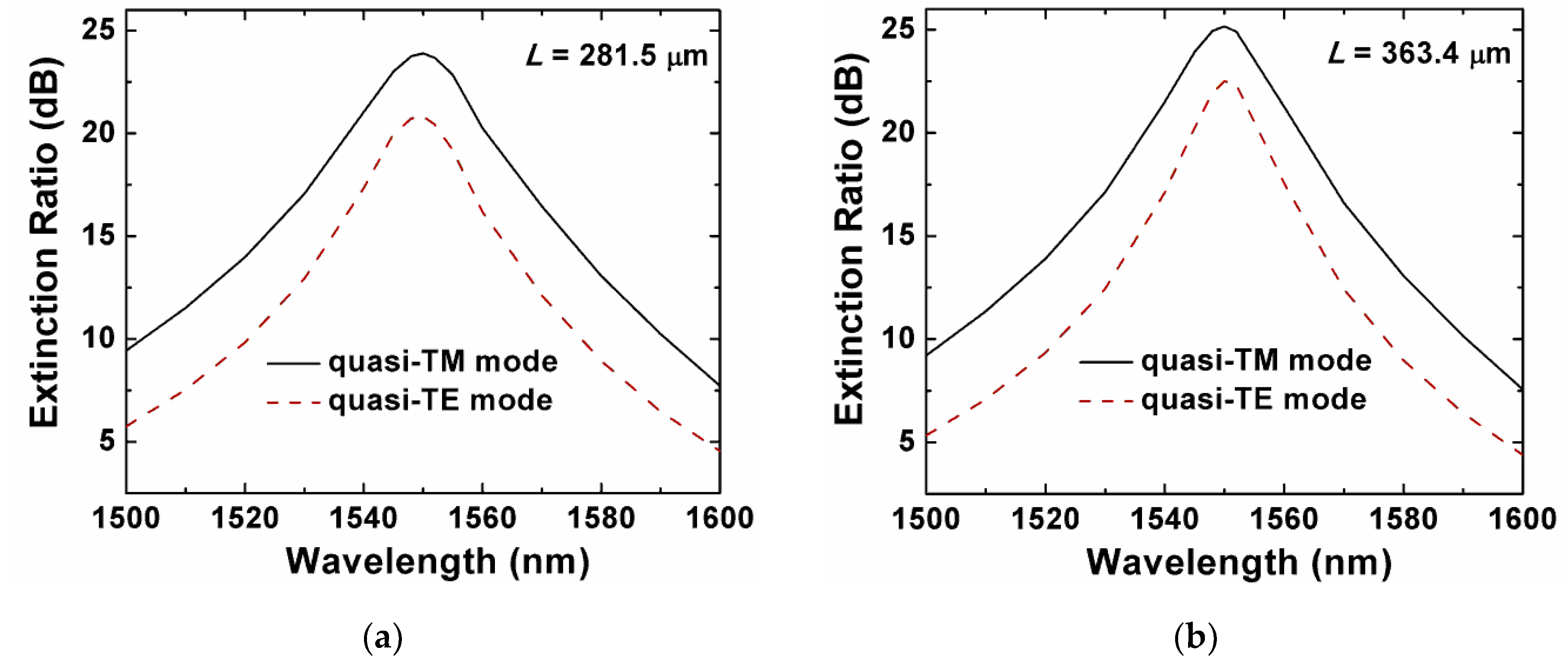
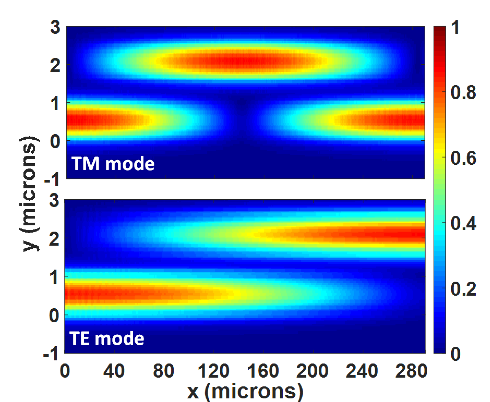
3.2. Single-Slot Waveguide Polarization Beam Splitter
3.3. Multi-Slot Waveguide Polarization Beam Splitter
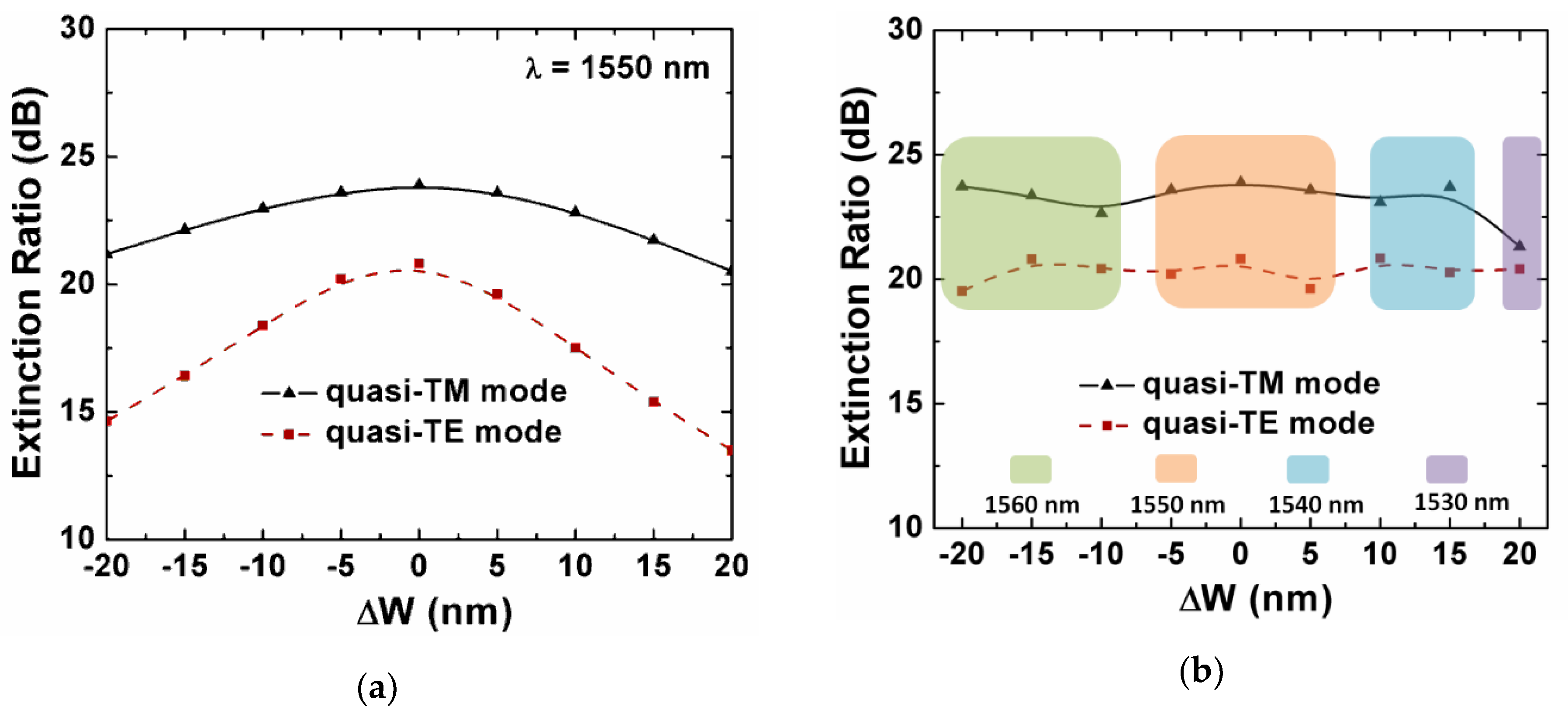
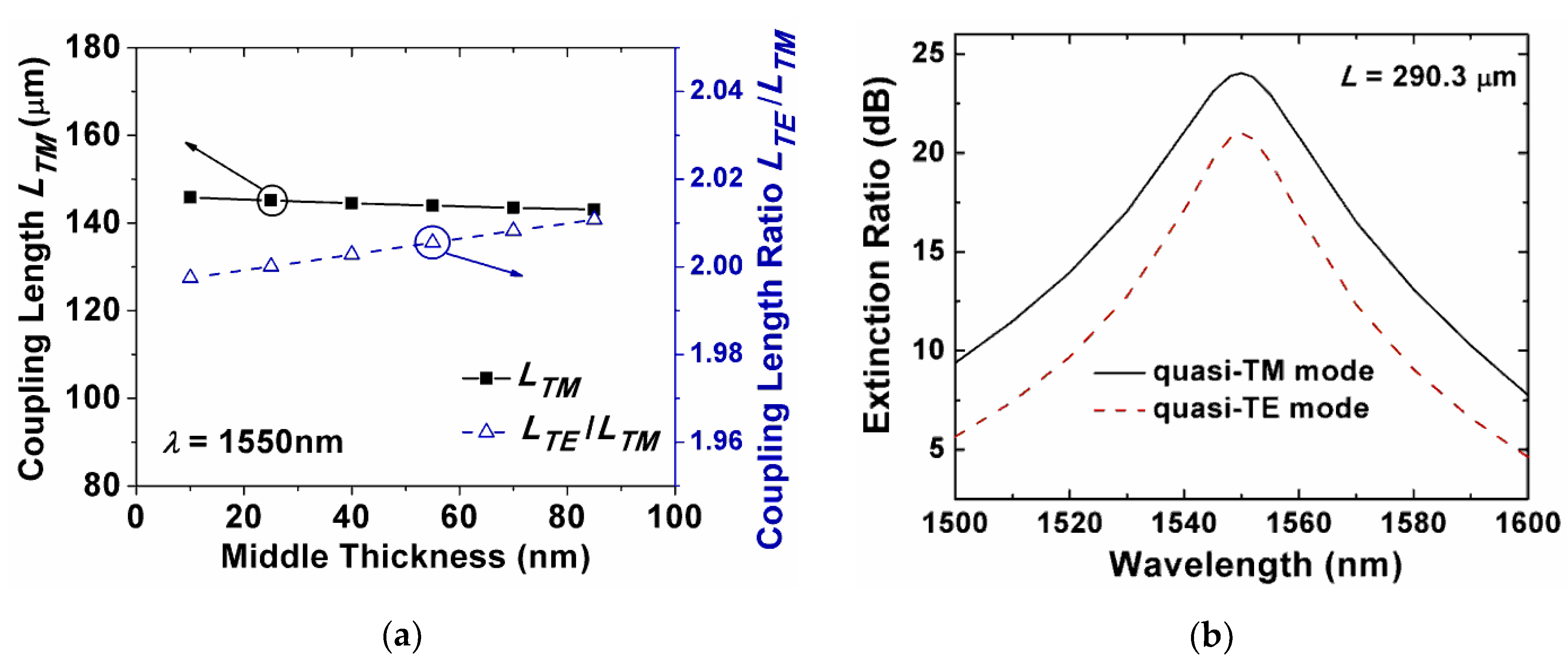
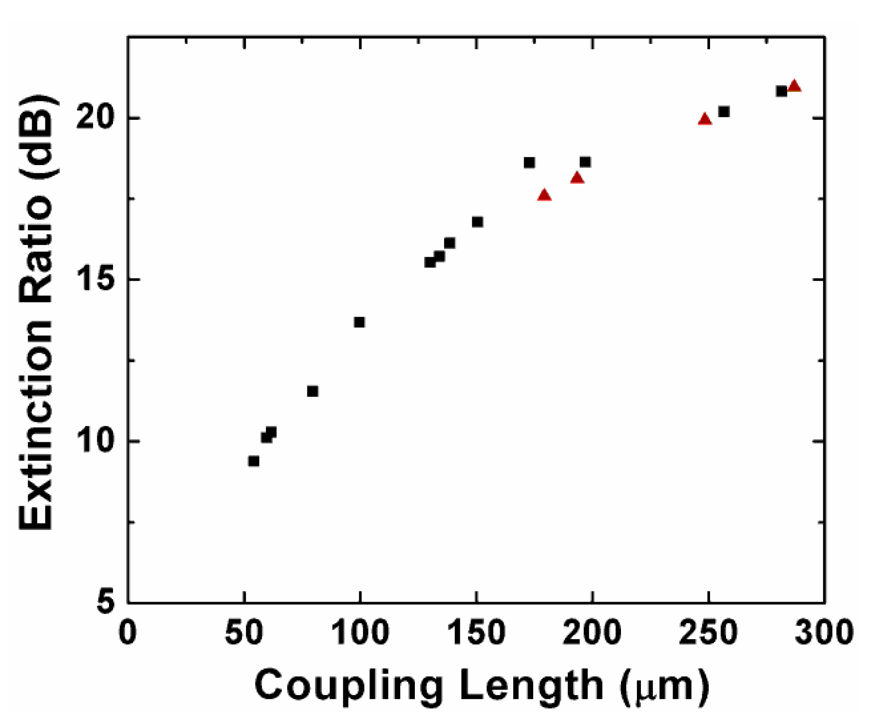
3.4. Tradeoff between the ER and Coupling Length
4. Conclusions
Author Contributions
Funding
Conflicts of Interest
References
- Asghari, M.; Krishnamoorthy, A.V. Silicon photonics: Energy-efficient communication. Nat. Photonics 2011, 5, 268–270. [Google Scholar] [CrossRef]
- Sun, C.; Wade, M.T.; Lee, Y.; Orcutt, J.S.; Alloatti, L.; Georgas, M.S.; Waterman, A.S.; Shainline, J.M.; Avizienis, R.R.; Lin, S.; et al. Single-chip microprocessor that communicates directly using light. Nature 2015, 528, 534–538. [Google Scholar] [CrossRef] [PubMed] [Green Version]
- Ikeda, K.; Saperstein, R.E.; Alic, N.; Fainman, Y. Thermal and Kerr nonlinear properties of plasma-deposited silicon nitride/silicon dioxide waveguides. Opt. Express 2008, 16, 12987–12994. [Google Scholar] [CrossRef] [PubMed] [Green Version]
- Tan, D.T.H.; Ikeda, K.; Sun, P.C.; Fainman, Y. Group velocity dispersion and self phase modulation in silicon nitride waveguides. Appl. Phys. Lett. 2010, 96, 061101. [Google Scholar] [CrossRef] [Green Version]
- Gorin, A.; Jaouad, A.; Grondin, E.; Aimez, V.; Charette, P. Fabrication of silicon nitride waveguides for visible-light using PECVD: A study of the effect of plasma frequency on optical properties. Opt. Express 2008, 16, 13509–13516. [Google Scholar] [CrossRef] [Green Version]
- Melchiorri, M.; Daldosso, N.; Sbrana, F.; Pavesi, L.; Pucker, G.; Kompocholis, C.; Bellutti, P.; Lui, A. Propagation losses of silicon nitride waveguides in the near-infrared range. Appl. Phys. Lett. 2005, 86, 121111. [Google Scholar] [CrossRef]
- Bauters, J.F.; Heck, M.J.R.; John, D.; Dai, D.; Tien, M.-C.; Barton, J.S.; Leinse, A.; Heideman, R.G.; Blumenthal, D.J.; Bowers, J.E. Ultra-low-loss high-aspect-ratio Si3N4 waveguides. Opt. Express 2011, 19, 3163–3174. [Google Scholar] [CrossRef]
- Li, Q.; Eftekhar, A.A.; Sodagar, M.; Xia, Z.; Atabaki, A.H.; Adib, A. Vertical integration of high-Q silicon nitride microresonators into silicon-on-insulator platform. Opt. Express 2013, 21, 18236–18248. [Google Scholar] [CrossRef]
- Lacava, C.; Stankovic, S.; Khokhar, A.Z.; Bucio, T.D.; Gardes, F.Y.; Reed, G.T.; Richardson, D.J.; Petropoulos, P. Si-rich Silicon Nitride for Nonlinear Signal Processing Applications. Sci. Rep. 2017, 7, 22. [Google Scholar] [CrossRef] [Green Version]
- Moss, D.J.; Morandotti, R.; Gaeta, L.A.; Lipson, M. New CMOS-compatible platforms based on silicon nitride and Hydex for nonlinear optics. Nat. Photonics 2013, 7, 597–607. [Google Scholar] [CrossRef] [Green Version]
- Bristow, A.D.; Rotenberg, N.; Driel, H.M.V. Two-photon absorption and Kerr coefficients of silicon for 850–2200 nm. Appl. Phys. Lett. 2007, 90, 191104. [Google Scholar] [CrossRef]
- Jalali, B. Nonlinear optics in the mid-infrared. Nat. Photonics 2010, 4, 506–508. [Google Scholar] [CrossRef]
- Lin, Q.; Zhang, J.; Piredda, G.; Boyd, R.W.; Fauchet, P.M.; Agrawal, G.P. Dispersion of silicon nonlinearities in the near-infrared region. Appl. Phys. Lett. 2007, 91, 021111. [Google Scholar] [CrossRef] [Green Version]
- Ferdous, F.; Miao, H.; Leaird, D.E.; Srinivasan, K.; Wan, J.; Chen, L.; Varghese, L.T.; Weiner, A.M. Spectral line-By-Line Pulse Shaping of On-Chip Microresonator Frequency Combs. Nat. Photonics 2011, 5, 1–2. [Google Scholar] [CrossRef]
- Hirose, K.; Liang, Y.; Kurosaka, Y.; Watanabe, A.; Sugiyama, T.; Noda, S. Watt-class high-power, high-beam-quality photonic-crystal lasers. Nat. Photonics 2014, 8, 406–411. [Google Scholar] [CrossRef]
- Sun, X.; Alam, M.Z.; Aitchison, J.S.; Mojahed, M. Compact and broadband polarization beam splitter based on a silicon nitride augmented low-index guiding structure. Opt. Lett. 2016, 41, 163–166. [Google Scholar] [CrossRef] [PubMed] [Green Version]
- Wu, H.; Tan, Y.; Dai, D. Ultra-broadband high-performance polarizing beam splitter on silicon. Opt. Express 2017, 25, 6069–6075. [Google Scholar] [CrossRef]
- Yue, Y.; Zhang, L.; Yang, J.-Y.; Beausoleil, R.G.; Willner, A.E. Silicon-on-insulator polarization splitter using two horizontally slotted waveguides. Opt. Lett. 2010, 35, 1364–1366. [Google Scholar] [CrossRef]
- Ong, J.; Ang, T.Ş.; Sahin, E.; Pawlina, B.; Chen, G.F.R.; Tan, D.T.H.; Limb, S.T.; Png, C.E. Broadband silicon polarization beam splitter with a high extinction ratio using a triple-bent-waveguide directional coupler. Opt. Lett. 2017, 42, 4450–4453. [Google Scholar] [CrossRef]
- Soudi, S.; Rahman, B.M.A. Compact Polarization Splitter by Using Identical Coupled Silicon Nanowires. J. Lightwave Technol. 2016, 34, 4168–4176. [Google Scholar] [CrossRef]
- Yang, J.; Du, T.; Niu, B.; Li, C.; Qian, J.; Guo, L. A Bionic Polarization Navigation Sensor Based on Polarizing Beam Splitter. IEEE Access 2018, 6, 11472–11481. [Google Scholar] [CrossRef]
- Hajireza, P.; Shi, W.; Bell, K.; Paproski, R.J.; Zemp, R.J. Non-interferometric photoacoustic remote sensing microscopy. Light-Sci. Appl. 2017, 6, e16278. [Google Scholar] [CrossRef] [PubMed]
- Qin, Z.; Zhu, T.; Chen, L.; Bao, X. High Sensitivity Distributed Vibration Sensor Based on Polarization-Maintaining Configurations of Phase-OTDR. IEEE Photonics Technol. Lett. 2011, 23, 1091–1093. [Google Scholar] [CrossRef]
- Li, X.; Ma, R.; Xia, Y. Magnetic Field Sensor Exploiting Light Polarization Modulation of Microfiber with Magnetic Fluid. J. Lightwave Technol. 2018, 36, 1620–1625. [Google Scholar] [CrossRef]
- Zhou, K.; Pan, S.; Liu, S.; Hu, K. Fiber gyroscope with a double sensitivity employing a polarization splitter. Opt. Lett. 2013, 38, 1337–1339. [Google Scholar] [CrossRef] [PubMed]
- Zhang, H.; Huang, Y.; Li, S.; Das., C.; Yu, M.; Lo, P.G.-Q.; Hong, M.; Thong, J. Polarization splitter using horizontal slot waveguide. Opt. Express 2013, 21, 3363–3369. [Google Scholar] [CrossRef]
- Zhang, Y.; He, Y.; Wu, J.; Jiang, X.; Liu, R.; Qiu, C.; Jiang, X.; Yang, J.; Tremblay, C.; Su, Y. High-extinction-ratio silicon polarization beam splitter with tolerance to waveguide width and coupling length variations. Opt. Express 2016, 24, 6586–6593. [Google Scholar] [CrossRef]
- Sun, X.; Aitchison, J.S.; Mojahedi, M. Realization of an ultra-compact polarization beam splitter using asymmetric MMI based on silicon nitride/silicon-on-insulator platform. Opt. Express 2017, 25, 8296–8305. [Google Scholar] [CrossRef]
- Lin, S.; Hu, J.; Crozier, K.B. Ultracompact, broadband slot waveguide polarization splitter. Appl. Phys. Lett. 2011, 98, 151101. [Google Scholar] [CrossRef]
- Cheng, N.-C.; Ma, Y.-F.; Fu, P.-H.; Chin, C.-C.; Huang, D.-W. Horizontal slot waveguides for polarization branching control. Appl. Opt. 2015, 54, 436–443. [Google Scholar] [CrossRef]
- Yin, X.; Xiao, J. A Compact TE-Pass Polarizer for Silicon-Based Slot Waveguides. IEEE Photonic Technol. Lett. 2015, 27, 2071–2074. [Google Scholar]
- Yin, X.; Xiao, J.; Sun, X. Design of a compact polarization demultiplexer for silicon-based slot waveguides. Appl. Opt. 2014, 53, 8305–8312. [Google Scholar]
- Yin, X.; Xiao, J.; Sun, X. Compact Polarization Beam Splitter for Silicon-Based Slot Waveguides Using an Asymmetrical Multimode Waveguide. J. Lightwave Technol. 2014, 32, 4884–4890. [Google Scholar] [CrossRef]
- Feng, J.; Akimoto, R.; Zeng, H. Asymmetric Silicon Slot-Waveguide-Assisted Polarizing Beam Splitter. IEEE Photonic Technol. Lett. 2016, 28, 1294–1297. [Google Scholar] [CrossRef]
- Liu, Y.; Chang, L.; Li, Z.; Liu, L.; Guan, H.; Li, Z. Polarization beam splitter based on a silicon nitride–silica–silicon horizontal slot waveguide. Opt. Lett. 2019, 44, 1335–1338. [Google Scholar] [CrossRef]
- Sun, R.; Dong, P.; Feng, N.; Hong, C.; Michel, J.; Lipson, M.; Kimerling, L. Horizontal single and multiple slot waveguides: Optical transmission at λ = 1550 nm. Opt. Express 2007, 15, 17968–17972. [Google Scholar] [CrossRef]
- Palik, E.D. Handbook of Optical Constants of Solids; Academic Press: San Diego, CA, USA, 1998. [Google Scholar]
- Baak, T. Silicon oxynitride; a material for GRIN optics. Appl. Opt. 1982, 21, 1069–1072. [Google Scholar] [CrossRef]
- Liang, T.-K.; Tsang, H.-K. Nonlinear Absorption and Raman Scattering in Silicon-on-Insulator Optical Waveguides. J. Sel. Top. Quantum Electron. 2004, 10, 1149–1153. [Google Scholar] [CrossRef]
- Roeloffzen, C.G.H.; Hoekman, M.; Klein, E.J.; Wevers, L.S.; Timens, R.B.; Marchenko, D.; Geskus, D.; Dekker, R.; Alippi, A.; Grootjans, R.; et al. Low-Loss Si3N4 TriPleX Optical Waveguides: Technology and Applications Overview. J. Sel. Top. Quantum Electron. 2018, 24, 1–21. [Google Scholar] [CrossRef] [Green Version]
- Zhang, L.; Agarwal, A.M.; Kimerling, L.C.; Michel, J. Nonlinear Group IV photonics based on silicon and germanium: From near-infrared to mid-infrared. Nanophotonics 2014, 3, 247–268. [Google Scholar] [CrossRef]
- Grassani, D.; Tagkoudi, E.; Guo, H.; Herkommer, C.; Yang, F.; Kippenberg, J.T.; Brès, C.-S. Mid infrared gas spectroscopy using efficient fiber laser driven photonic chip-based supercontinuum. Nat. Commun. 2019, 10, 1553. [Google Scholar] [CrossRef] [PubMed] [Green Version]
- Afshar, S.; Monro, T.M. A full vectorial model for pulse propagation in emerging waveguides with subwavelength structures part I: Kerr nonlinearity. Opt. Express 2009, 17, 2298–2318. [Google Scholar] [CrossRef] [PubMed] [Green Version]
- Kim, K.S.; Stolen, R.H.; Reed, W.A.; Quoi, K.W. Measurement of the nonlinear index of silica-core and dispersion shifted fibers. Opt. Lett. 1994, 19, 257–259. [Google Scholar] [CrossRef] [PubMed]
- Dinu, M.; Quochi, F.; Garcia, H. Third-order nonlinearities in silicon at telecom wavelengths. Appl. Phys. Lett. 2003, 82, 2954–2956. [Google Scholar] [CrossRef]
- Bozinovic, N.; Yue, Y.; Ren, Y.; Tur, M.; Kristensen, P.; Huang, H.; Willner, A.E.; Ramachandran, S. Terabit-Scale Orbital Angular Momentum Mode Division Multiplexing in Fibers. Science 2013, 340, 1545–1548. [Google Scholar] [CrossRef] [Green Version]
- Feng, N.-N.; Michel, J.; Kimerling, L.C. Optical Field Concentration in Low-Index Waveguides. IEEE J. Quantum Electron. 2006, 42, 885–890. [Google Scholar] [CrossRef]
- Jiang, W.; Sun, X.; Rahman, B.M.A. Compact and fabrication-tolerant polarization splitter based on horizontal triple-slot waveguide. Appl. Opt. 2017, 56, 2119–2126. [Google Scholar] [CrossRef]


| H (nm) | W (nm) | Hs (nm) | Hu (nm) | d (nm) | LTE/LTM | LTE (μm) | ER (dB) |
|---|---|---|---|---|---|---|---|
| 620 | 1200 | 100 | 260 | 200 | 2.0015 | 54.20 | 9.38 |
| 780 | 1150 | 100 | 410 | 200 | 2.0022 | 59.74 | 10.12 |
| 800 | 1150 | 90 | 410 | 200 | 1.9985 | 61.69 | 10.29 |
| 1200 | 1200 | 300 | 260 | 200 | 2.0040 | 79.48 | 11.54 |
| 840 | 1100 | 90 | 300 | 300 | 1.9995 | 99.75 | 13.68 |
| 950 | 1100 | 150 | 300 | 350 | 2.0001 | 130.14 | 15.53 |
| 1000 | 1100 | 150 | 340 | 350 | 1.9991 | 134.13 | 15.72 |
| 950 | 1050 | 150 | 410 | 400 | 1.9974 | 138.59 | 16.12 |
| 950 | 1050 | 120 | 440 | 400 | 1.9995 | 150.57 | 16.78 |
| 720 | 1000 | 90 | 250 | 500 | 1.9963 | 172.86 | 18.62 |
| 800 | 1000 | 90 | 390 | 500 | 2.0001 | 196.96 | 18.63 |
| 830 | 1050 | 90 | 250 | 500 | 2.0027 | 256.65 | 20.19 |
| 800 | 1050 | 50 | 250 | 500 | 2.0035 | 281.46 | 20.82 |
| H (nm) | W (nm) | Hs (nm) | Hu (nm) | Hm (nm) | d (nm) | LTE/LTM | LTE (μm) | ER (dB) |
|---|---|---|---|---|---|---|---|---|
| 840 | 1050 | 100 | 150 | 150 | 500 | 1.9990 | 179.29 | 17.58 |
| 840 | 1050 | 90 | 150 | 150 | 500 | 2.0041 | 193.41 | 18.12 |
| 800 | 1050 | 70 | 50 | 100 | 500 | 1.9966 | 248.44 | 19.93 |
| 830 | 1050 | 25 | 250 | 120 | 500 | 2.0017 | 286.89 | 20.95 |
© 2020 by the authors. Licensee MDPI, Basel, Switzerland. This article is an open access article distributed under the terms and conditions of the Creative Commons Attribution (CC BY) license (http://creativecommons.org/licenses/by/4.0/).
Share and Cite
Fang, Y.; Bao, C.; Wang, Z.; Liu, Y.; Zhang, L.; Huang, H.; Ren, Y.; Pan, Z.; Yue, Y. Polarization Beam Splitter Based on Si3N4/SiO2 Horizontal Slot Waveguides for On-Chip High-Power Applications. Sensors 2020, 20, 2862. https://doi.org/10.3390/s20102862
Fang Y, Bao C, Wang Z, Liu Y, Zhang L, Huang H, Ren Y, Pan Z, Yue Y. Polarization Beam Splitter Based on Si3N4/SiO2 Horizontal Slot Waveguides for On-Chip High-Power Applications. Sensors. 2020; 20(10):2862. https://doi.org/10.3390/s20102862
Chicago/Turabian StyleFang, Yuxi, Changjing Bao, Zhonghan Wang, Yange Liu, Lin Zhang, Hao Huang, Yongxiong Ren, Zhongqi Pan, and Yang Yue. 2020. "Polarization Beam Splitter Based on Si3N4/SiO2 Horizontal Slot Waveguides for On-Chip High-Power Applications" Sensors 20, no. 10: 2862. https://doi.org/10.3390/s20102862