A High Resolution On-Chip Delay Sensor with Low Supply-Voltage Sensitivity for High-Performance Electronic Systems

Abstract
: An all-digital on-chip delay sensor (OCDS) circuit with high delay-measurement resolution and low supply-voltage sensitivity for efficient detection and diagnosis in high-performance electronic system applications is presented. Based on the proposed delay measurement scheme, the quantization resolution of the proposed OCDS can be reduced to several picoseconds. Additionally, the proposed cascade-stage delay measurement circuit can enhance immunity to supply-voltage variations of the delay measurement resolution without extra self-biasing or calibration circuits. Simulation results show that the delay measurement resolution can be improved to 1.2 ps; the average delay resolution variation is 0.55% with supply-voltage variations of ±10%. Moreover, the proposed delay sensor can be implemented in an all-digital manner, making it very suitable for high-performance electronic system applications as well as system-level integration.1. Introduction
As semiconductor device size decreases, and the performance requirements of electronic products increase, the operating frequencies of advanced electronic systems can exceed several gigahertz, leading to narrower timing margins in the digital circuit. In the high-level integration systems, including system-on-chip (SoC), system-in-package (SiP), and 3D IC, the delay uncertainties, such as propagation delay mismatching, clock skew and jitter, degrade overall system performance and increase design efforts to meet the timing constraints; thus, these uncertainties cannot be ignored—particularly when small timing margins exist [1–5]. Furthermore, the timing-related defects that are caused by manufacturing-process-related problems, such as resistive opens and shorts, device mismatches, etc., become serious problems [1,3,6]. Besides, non-ideal effects, such as negative bias temperature instability (NBTI), hot career injection (HCI), and electromigration (EM), will induce serious reliability issues after shipment [6,7]. Consequently, to ensure the functionality and performance of high-performing systems, it is necessary to develop a technology that measures either the delay in the critical path or timing uncertainty in the circuit [1–8].
Traditionally, delays can characterized by the off-chip method. However, because the accuracy of off-chip delay measurement is dominated by parasitic capacitance, probe resistance, and transmission line impedance, it is not suitable for internal nodes whose required timing resolution is at the picosecond level as the timing margin narrows. Besides, the increasing complexities of electronic systems limit the accessibility of internal circuit modules [2,5]. Thus, an on-chip delay sensor (OCDS) that can provide debugging for internal chip performance failure and delay diagnosis for high-frequency system applications is necessary. Moreover, at-speed delay measurements can provide the information required to improve overall performance and reduce the power consumption of equipment with dynamic voltage and frequency scaling (DVFS) schemes [8,9].
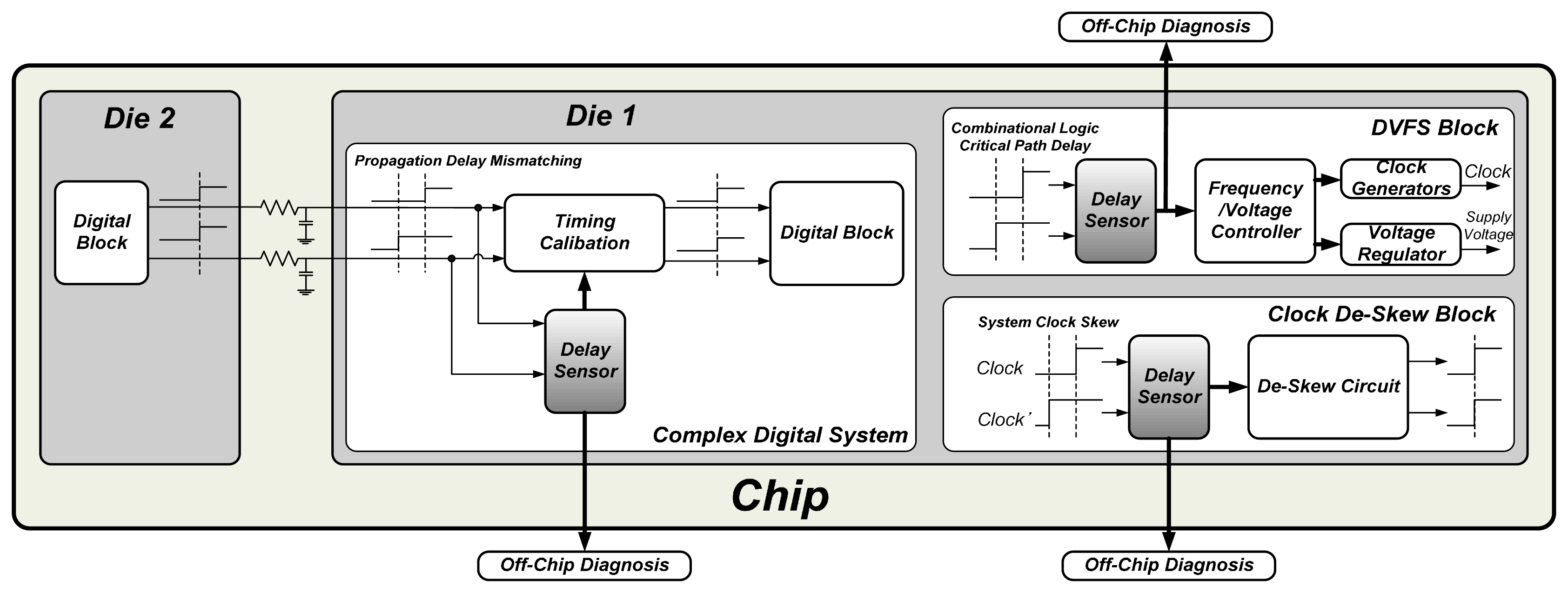
The scope of OCDS applications is illustrated in Figure 1. For example, the OCDS can detect the propagation delay mismatching between dies, and provide the sensing information for timing calibration or off-chip diagnosis. In the DVFS system, an OCDS circuit can measure the specified timing-critical path delay in a digital block and provide such delay information to the frequency/voltage controller. Based on the measured delay provided by the OCDS circuit, the operating frequency and supply voltage of the chip can be adjusted to improve overall performance and reduce power consumption. In addition to the timing-critical path delay measurement, the OCDS module can measure the clock skew between different clocks and output the measured data for clock de-skew circuit or diagnosis in an off-chip tester machine. Generally, because the considered transmission path and clock signal can be specified during the design phase, the number and location of the OCDS modules can be determined before chip fabrication.
Different approaches have been developed to implement an OCDS. The time-to-digital converter (TDC) can convert the measured delay to digital code. The design concept of TDC is very straightforward; however, its quantization resolution is not sufficient for advance system applications [10,11]. In contrast to TDC, measurement circuits based on a Vernier delay line (VDL) can achieve high delay resolution. However, such circuits have large hardware costs, and their delay resolutions are sensitive to supply-voltage variations [5,12]. A path-based ring oscillator structure that converts the target path's delay to the oscillation period has been proposed [13]. Although this architecture can be integrated into current design-for-testability (DFT) flow, its resolution is restricted by the oscillation period. To improve this delay resolution, an analogously tunable delay line, whose delay can be controlled with an analogous voltage, has been proposed [14]. This design can provide high delay resolution; however, it requires an additional high-quality digital-to-analog (DAC) circuit, which increases hardware costs and design effort. A differential delay line pair structure that provides high delay resolution has been proposed [15]. However, the detection range is insufficient for die-to-die timing calibration.
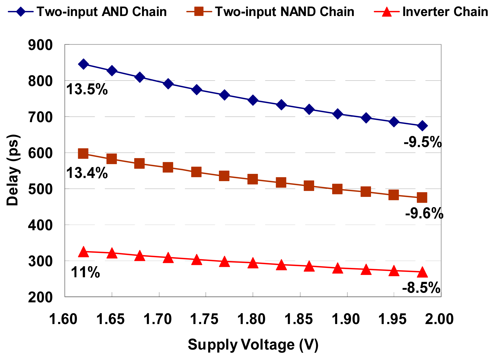
The most important criterion of OCDS is its quantization resolution and timing quantization stability, both of which determine the accuracy and quality of its delay measurement. Basically, the digital approach utilizes the delay cell's delay, such as the buffer or AND gate, as the overall quantization resolution. Unfortunately, in the complementary metal-oxide-semiconductor (CMOS) process, gate delay is strongly affected by supply-voltage variations. Figure 2 shows the delay spread of a delay line composed of 10 basic logic gates connected in a series in a 0.18 μm CMOS process. For example, in the two-input AND delay chain, the delay varies widely from 675 to 846.4 ps with ±10% supply-voltage variations, which means the percentages of the delay variation value are −9.5% and 13.5%. In complex digital systems, the supply voltage of OCDS varies easily due to nearby circuit influences or other non-ideal effects; therefore, the delay resolution of the delay line is unpredictable and unstable. Consequently, the measurement accuracy of OCDS is significantly degraded by supply-voltage variations, and OCDS with low immunity to supply variations is unsuitable for in-demand high-precision applications.
In this paper, an all-digital, high-resolution OCDS circuit with high immunity to supply-voltage variations is proposed for high-performance electronic system applications. The proposed OCDS uses a novel, closed-loop delay measurement to provide high delay-measurement resolution. Furthermore, the proposed OCDS employs a cascade-stage delay measurement circuit, including a coarse delay measurement stage (CDMS) and two fine delay measurement stages (FDMS), and a high-sensitivity phase detector (PD) to enhance the immunity of the overall delay resolution to supply-voltage variations. Moreover, the complete design of the proposed OCDS can be implemented in an all-digital manner, making its integration into a digital system easy.
This paper is organized as follows: Section 2 describes the proposed delay measurement scheme and hardware architecture. Section 3 focuses on the key module circuit design of OCDS, including CDMS, FDMS, and PD. In Section 4, the implementation and simulation results of the proposed design are presented. Finally, the conclusions are addressed in Section 5.
2. Sensor Overview
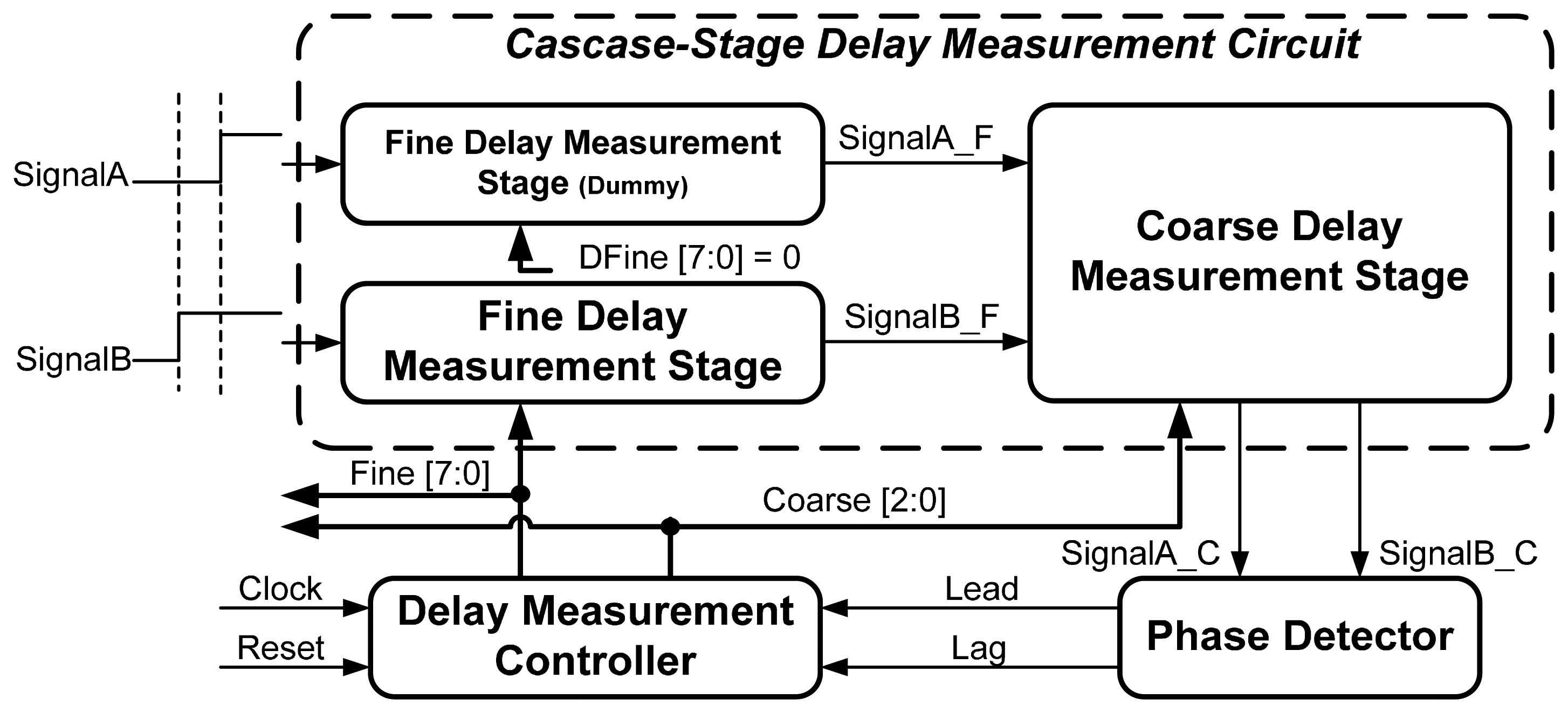
Figure 3 illustrates the proposed all-digital OCDS architecture, which comprises a cascade-stage delay measurement circuit, a PD, and a delay measurement controller. The proposed cascade-stage delay measurement circuit comprises a CDMS, a FDMS, and a dummy fine delay measurement stage. The coarse and fine delay measurement stages form the controllable delay line with different tunable delay steps. The CDMS has coarse quantization resolution, and the delay is controlled by the coarse control code Coarse[2:0]. In contrast to the CDMS, the FDMS has a smaller controllable delay to increase the overall delay measurement resolution, and the delay of the fine measurement stage is controlled by the fine control code Fine[7:0]. To maintain intrinsic delay matching during delay measurement, the dummy FDMS whose control code (DFine[7:0]) is fixed to zero is added. If the timing difference between SignalA and SignalB requires measurement, SignalA and SignalB are sent to cascade-stage delay measurement as inputs of the dummy fine measurement stage and fine measurement stage, respectively.
After SignalA and SignalB propagate through the fine delay measurement stages, the first delayed version signals (SignalA_F and SignalB_F) are sent to the CDMS, which generates the second delayed version signals (SignalA_C and SignalB_C). Based on the phase polarity between SignalA_C and SignalB_C, the phase detector generates the phase comparison results Lead and Lag. According to the phase comparison results, the measurement controller changes digital control codes to tune the CDMS and FDMS delays until the phases of SignalA_C and SignalB_C align.
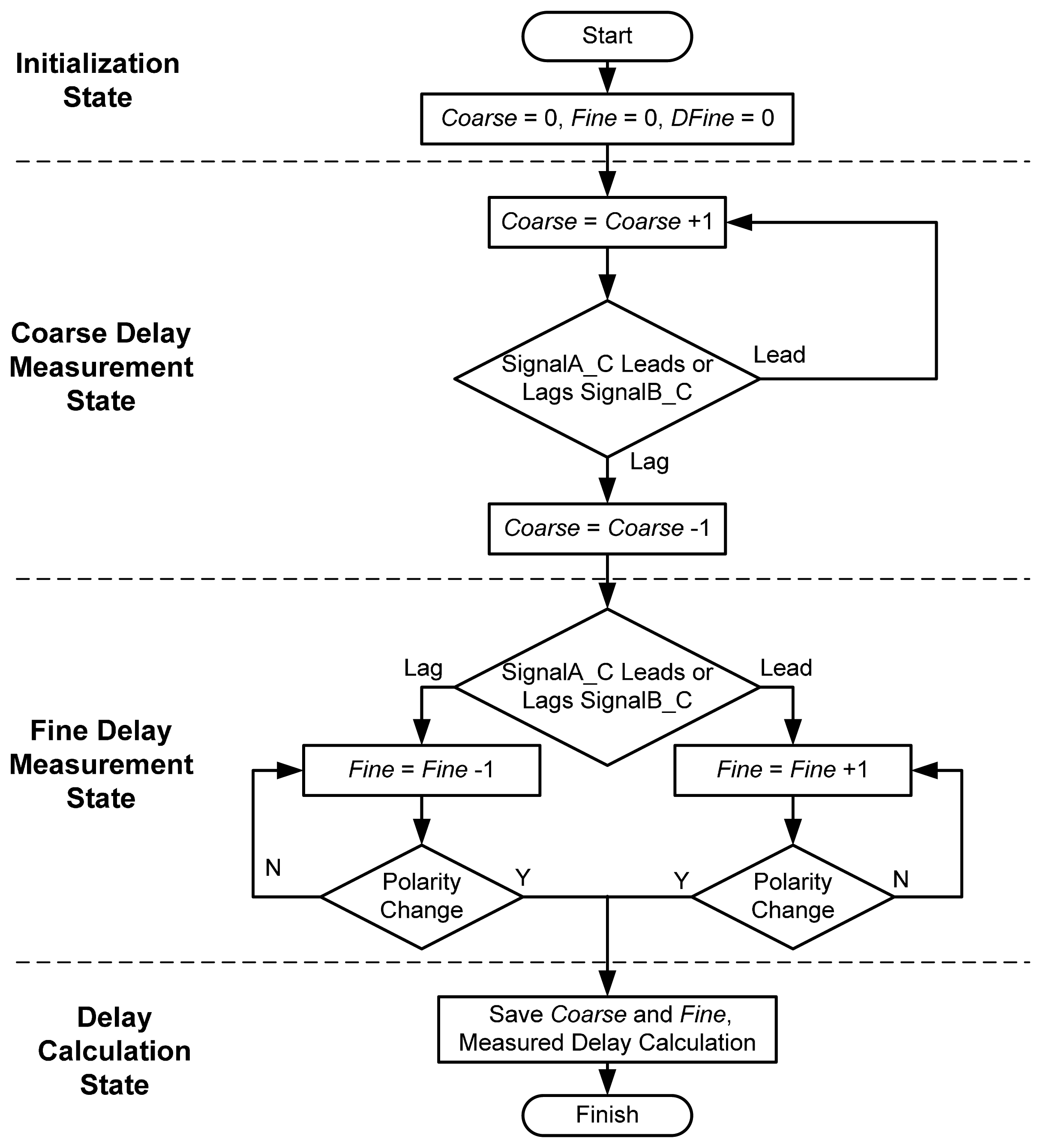
The flowchart of the proposed OCDS is shown in Figure 4. The entire delay measurement process is divided into coarse and fine measurement states. In the beginning, two control codes, Coarse and Fine, are initialized to zero. Subsequently, the phase detector asserts a digital signal, either Lead or Lag, based on the phase polarity of the SignalA_C rising edge to the SignalB_C rising edge. We assume that the positive edge of SignalA leads the positive edge of SignalB; therefore, in the beginning, the positive edge of SignalA_C will lead the positive edge of SignalB_C. Subsequently, the phase detector asserts Lead, and the delay measurement controller increases Coarse by one to enlarge the propagation delay from SignalB_F to SignalB_C until the positive edge of SignalA_C lags behind that of SignalB_C. Once the phase detector senses a change in the phase polarity of SignalA_C relative to SignalB_C, the delay measurement controller decreases Coarse by one, and the coarse measurement state is complete.
The operation of the fine delay measurement state and coarse delay measurement state are similar. In the fine delay measurement state, the delay measurement controller determines Fine to change the propagation delay from SignalB to SignalB_F. If the positive edge of SignalA_C leads that of SignalB_C, the measurement controller increases Fine by one to enlarge the propagation delay from SignalB to SignalB_F. Conversely, if the phase detector asserts Lag, the delay measurement controller decreases Fine by one to reduce the propagation delay from SignalB to SignalB_F. Phase comparison continues until the phase detector senses a change in the phase polarity of SignalA_C relative to SignalB_C. At this point, Coarse and Fine will be saved, and the delay measurement is complete.
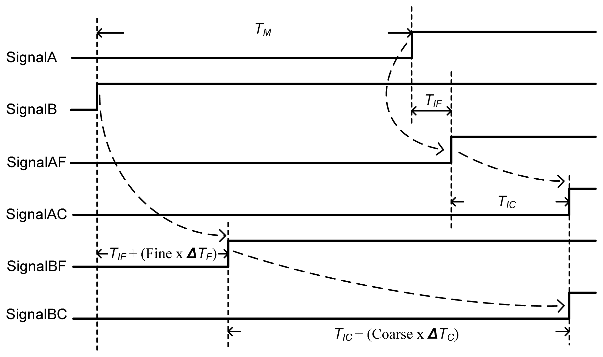
Because the positive edges of SignalA_C and SignalB_C will be aligned after the delay measurement is complete, the delay between SignalA and SignalB is equal to the propagation delay difference between SignalA to SignalA_C and SignalB to SignalB_C, which can be formulated as:
ÄTC and ÄTF are the quantization resolution (delay step) of CDMS and FDMS, respectively. TIC and TIF are the intrinsic delay of CDMS and FDMS, respectively. According to Equations (1) and (2), the delay between SignalA and SignalB (TM) can be quantized by the FDMS's finest delay step, and the measured delay can be calculated by the quantization resolution, Coarse, and Fine, as shown in Figure 5. It can be formulated as:
The relationship between the delay steps of CDMS and those of FDMS is stable in the proposed cascade-stage delay measurement circuit. Moreover, according to Equation (4), the quantization resolution of the OCDS circuit is equal to ÄTF. Thus, if ÄTF is insensitive to supply-voltage variations, the same measured delay (TM) will have the same quantization results (Coarse and Fine) when supply-voltage variations are present. As a result, the delay measurement results of the OCDS will not be affected by supply-voltage variations. The rest of this paper describes how to implement a high quantization resolution OCDS whose finest delay step is insensitive to supply-voltage variations.
3. Circuit Implementation
3.1. Coarse Delay Measurement Stage
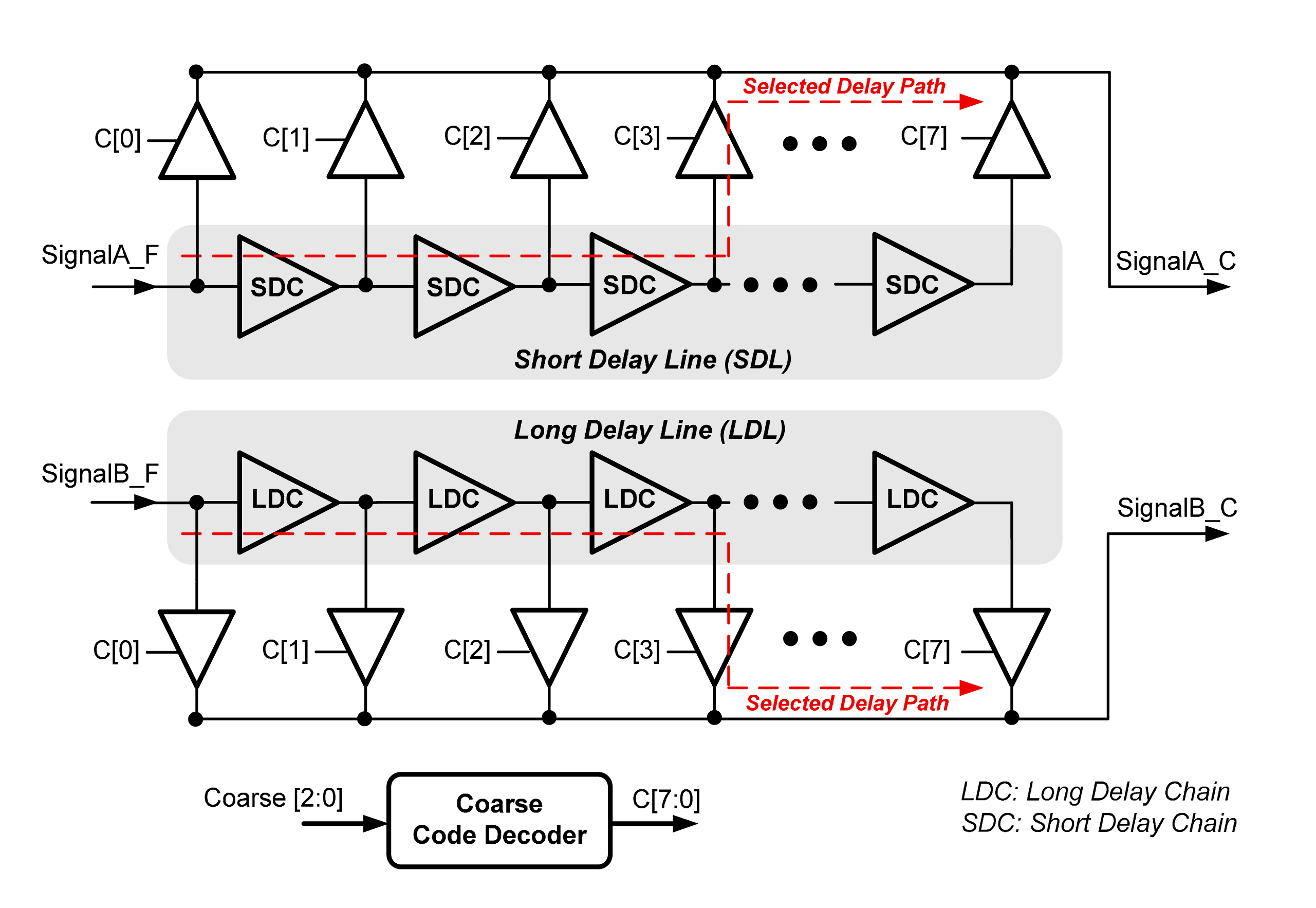
The proposed CDMS is composed of a long delay line, short delay line, coarse code decoder, and sixteen tri-state buffers, as shown in Figure 6. The long and short delay line comprise seven long delay chains (LDC) and seven short delay chains (SDC), respectively. The proposed coarse code decoder receives Coarse[2:0] from the delay measurement controller and generates path selection signals C[7:0] to the tri-state buffers. The coarse code decoder converts binary code to one-shot code. As SignalA_F propagates through short delay line, it can provide eight different delay values by selecting different delay paths organized by these seven SDCs. Similar to SignalA_F, SignalB_F propagates through long delay line and a turned-on tri-state buffer (determined by C[7:0]) to SignalB_C. Based on the CDMS's circuit structure, the propagation delays of SignalA_F to SignalA_C (TAC) and SignalB_F to SignalB_C (TBC) can be formulated as:
3.2. Delay Cell
In the proposed OCDS design, the most important design consideration is how to maintain measurement accuracy when supply-voltage variations exist. Because measurement accuracy is determined by the stability of the delay cell in cascade-stage delay measurement circuit, it is important to enhance the immunity that CDMS and FDMS delay quantization resolutions have to supply-voltage variations. According to Equation (6), the delay quantization resolution of CDMS is determined by the delay difference between the LDC and SDC. Thus, if the delay difference between the LDC and SDC is insensitive to supply-voltage variations, the stability and accuracy of the CDMS's measurement can be ensured.
When the supply voltage change, the propagation delay of the LDC and SDC can be formulated as:
TLDC1 and TSDC1 are the propagation delays the LDC and SDC, respectively, after supply changes. TLDC0 and TSDC0 are the propagation delays the LDC and SDC, respectively, before supply changes. ΔTLDC and ΔTSDC are the delay variations of the LDC and SDC, respectively, caused by supply changes. If ΔTLDC is equal to ΔTSDC, the delay difference between the LDC and SDC (ΔTC) will maintain a constant value under different supply voltages, as shown in Equations (7) and (8).
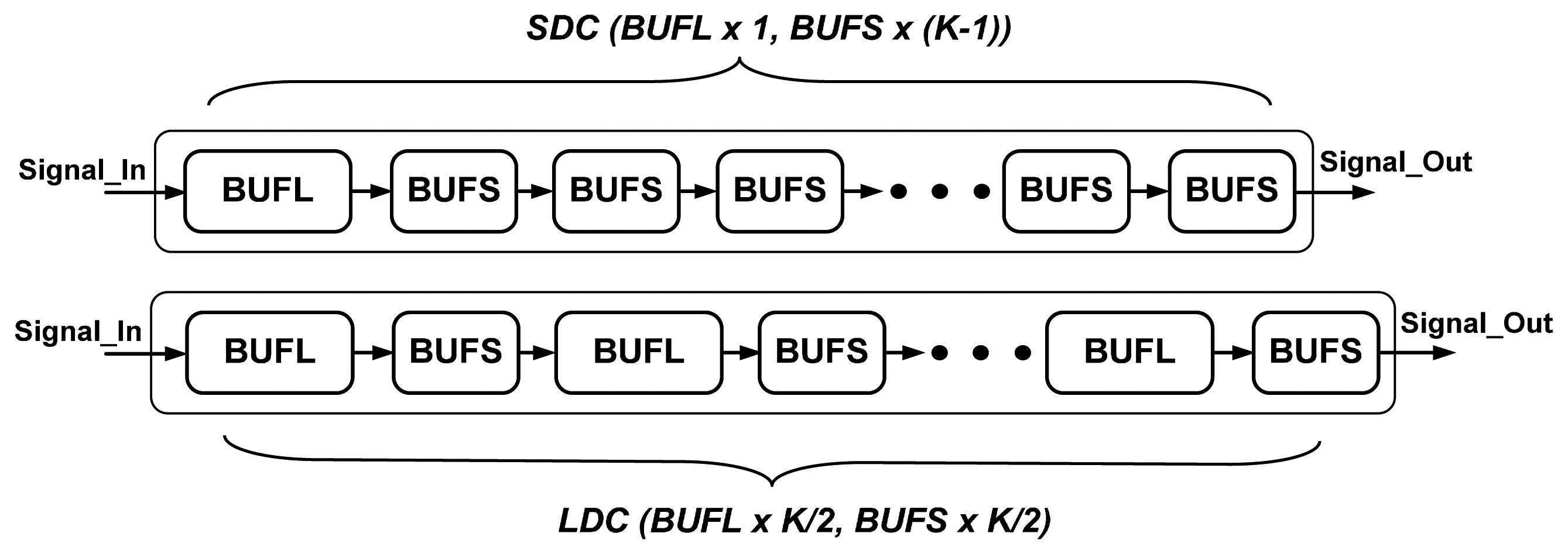
The circuit diagrams of the proposed LDC and SDC are shown in Figure 7. The proposed LDC comprises K/2 large (BUFL) and K/2 small buffers (BUFS). The proposed SDC comprises one large (BUFL) and K − 1 small buffers (BUFS). The large and small buffers determine not only the LDC and SDC overall delays, but also the delay variations caused by supply changes. The large and small buffers are rise/fall times balance buffers and have the same circuit structure; the only difference between them is the channel width and length of each MOS, which leads to different obtained delays. If the LDC and SDC use the same buffer, both delay variations caused by supply changes will be the same. However, these two delay cells also have the same propagation delay, which is not suitable for CDMS requirements.
Thus, at first, the LDC and SDC comprise K large and K small buffers, respectively. In order to reduce the delay variation difference between the LDC and SDC caused by supply changes, K/2 large buffers are replaced by K/2 small buffers in the LDC. Furthermore, K/2 large and K/2 small buffers have interleaved placement. The first small buffer in the SDC is replaced by a large buffer so that LDC and SDC have the same driving capability. The LDC and SDC delays need to be characterized under different supply voltages in the HSPICE simulation, and maintaining the delay difference between the LDC and SDC requires a constant value under different supply voltages, as shown in Equation (8).
The implementation of the BUFL and BUFS, as used in the proposed long delay and short chains, is a challenge in our design. We propose a systematic design flow to determine the transistor sizes and the layout style of the buffer to improve performance. The flowchart of the proposed design flow is shown in Figure 8. In order to reduce the design and layout complexity, we use the delay cells from the standard cell library. In the beginning, one type of delay cell in the standard cell library is selected. After the layout, the delays of all the buffers different driving capability are characterized as a function of supply voltage variation. Based on the delay characterization results, the suitable buffers can be selected for the long and short delay chains. Finally, if ΔTLDC is equal to ΔTSDC, ΔTC will maintain a constant value under different supply voltages. If not, another buffer for the long and short delay chains must be selected until our design target is achieved.
3.3. Fine Delay Measurement Stage
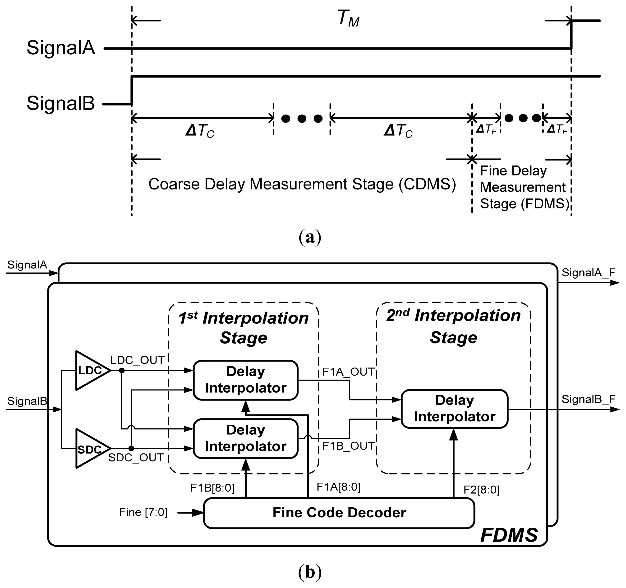
Although the delay quantization resolution of CDMS can maintain a constant value when the supply voltage changes, it is still insufficient for high-performance system applications. Thus, an FDMS is added to the proposed cascade-stage delay measurement circuit to improve the overall delay quantization resolution from one gate delay to several picoseconds. The operation concept of the proposed cascade-stage delay measurement circuit is illustrated in Figure 9a. The delay between SignalA and SignalB will be measured by the CDMS and FDMS. After the CDMS measures, the time residue will be measured by FDMS to further improve the measurement quantization. In order to maintain immunity to supply-voltage variations, the ratio of delay quantization resolution in the CDMS to that in FDMS has to maintain a constant value, and the delay quantization resolution of FDMS should also have a high immunity to supply-voltage variations.
The proposed FDMS is composed of an LDC, SDC, first interpolation stage, second interpolation stage, and fine code decode, as shown in Figure 9b. The proposed FDMS employs a two-stage delay interpolation structure—the inputs that SignalA and SignalB send to the corresponding FDMS, respectively—to improve the delay quantization resolutions. Because the propagation path of two input signals is the same, they have the same intrinsic delay. If the positive edge of SignalA leads the positive edge of SignalB, the fine control code for FDMS that SignalA passed will be set to zero (DFine[7:0]). Meanwhile, the fine control code for FDMS that SignalB passed will be increased to reduce the phase difference between SignalA_F and SignalB_F.
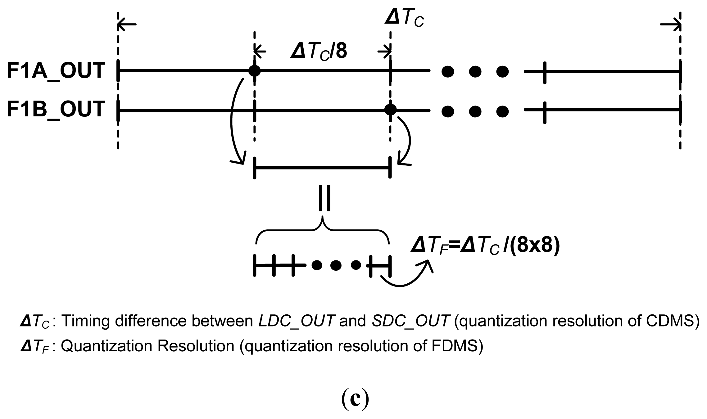
Because the delay interpolator can divide the delay between two input signals into equal parts, if the timing difference between LDC_OUT and SDC_OUT is ΔTC and the interpolation step of the first and second interpolation stages are Q and R, respectively, the overall delay resolution of the OCDS will be ΔTC/(Q × R), as shown in Figure 8c. According to the design specification, the design parameters are determined as follows: Q = 8 and R = 8. The first interpolation stage receives LDC_OUT and SDC_OUT from the LDC and SDC, respectively, and then interpolates those signals to generate two signals (F1A_OUT and F1B_OUT). The delays of the first and second interpolation stages are controlled by {F1A[8:0], F1B[8:0]} and F2[8:0], respectively, which are generated by the code decoders.
Figure 10 illustrates the architecture of the proposed first interpolation stage, which comprises two delay interpolators [16]. Each delay interpolator comprises two driving groups: Group I–IV. The proposed first interpolation stage generates two outputs (F1A_OUT and F1B_OUT) whose timing difference is one 1st tuning delay step. Table 1 lists the combinations of the four control group codes. The single delay step of the first interpolation stage has been “extracted” by the 1st tuning control code; the second interpolation stage receives these two outputs and further improves delay resolution by the delay interpolator.
Because the delay difference between the LDC and SDC (ΔTC) and the interpolation step of two interpolation stages (8, 8) are not affected by supply variation, the overall delay quantization resolution of the proposed OCDS (ΔTC/(8 × 8)) is insensitive to supply-voltage variations. As a result, the proposed OCDS can not only achieve high delay resolution, it can also have a high immunity to supply-voltage variations.
3.4. Phase Detector
In order to improve measurement accuracy, the proposed OCDS employs a sense-amplifier-based PD to ensure that the overall delay resolution will not be reduced by the PD's dead zone [17]. Based on simulation results, the sense-amplifier-based PD can detect a phase error greater than 1 ps; thus, it is very suitable for the proposed OCDS design.
4. Simulation Results
The proposed all-digital OCDS is implemented in a 0.18 μm 1P6M CMOS process. The design parameters of the proposed cascade-stage delay measurement circuit are determined on the basis of requested delay measurement resolution that is based on our application. The layout of the OCDS is shown in Figure 11; its area is 1038 μm × 358 μm.
The proposed OCDS is designed and implemented using an all-digital design flow; thus, the proposed architecture and algorithm are modeled in the hardware description language (HDL) and the functionally is verified using an NC-Verilog simulator. Figure 12a,b show the quantization process of the coarse and fine delay measurement, respectively. The simulation results of the proposed OCDS scheme show that the target measured delay is converted to the quantization value. The entire delay measurement process is divided into coarse and fine measurement states. In the beginning, two control codes, Coarse and Fine, are initialized to zero. If the positive edge of SignalA leads the positive edge of SignalB, the delay measurement controller increases Coarse by one to enlarge the propagation delay from SignalB_F to SignalB_C until the phase detector senses a change in the phase polarity. The delay measurement controller decreases Coarse by one, and the coarse measurement state is complete. In the fine delay measurement state, if the positive edge of SignalA leads the positive edge of SignalB, the measurement controller increases Fine by one to enlarge the propagation delay from SignalB to SignalB_F. Phase comparison continues until the phase detector senses a change in the phase polarity. At this point, Coarse and Fine will be saved, and the delay measurement is complete.
In order to verify the performance of the proposed OCDS precisely, post-layout simulation of the timing-related part uses HSPICE for enhanced accuracy. To test the delay measurement characteristic of the proposed OCDS, input time intervals of 0–600 ps with a 25 ps step are applied to the system. The simulation shows the measurement characteristic with ±10% supply-voltage variations (from 1.62 V to 1.98 V). The average measurement resolution is 1.2 ps. The measured delay can be obtained from the output digital code by measurement resolution. The output digital code comprises Coarse and Fine. Because the delay quantization resolution of Coarse is 64 times that of Fine, Coarse needs to multiply by 64, combine with Fine, and then convert to decimal-format digital code. For example, if Coarse is 2 and Fine is 32, the output digital code is equal to 160 (2 × 64 + 32) and the measured delay is 192 ps (160 × 1.2 ps).
To evaluate supply-voltage sensitivity, the resolution deviation of the system is determined by simulation over a supply-voltage range of 1.8 V ± 10%. Figure 13 shows the simulation results for supply voltages ranging from 1.62 V to 1.98 V in 0.05 V steps, presenting an average 0.55% and maximum 1.1% resolution deviation over the specified supply voltage range. The corresponding measurement error and differential nonlinearity (DNL) are also calculated to evaluate the linearity of the system, as shown in Figures 14 and 15, respectively. DNL errors of less than 0.72 LSB, 0.6 LSB, and 0.63 LSB with supply voltages of 1.8 V, 1.98 V, and 1.62 V, respectively, are obtained.
Table 2 lists comparison results with state-of-the-art OCDSs for electronic system applications. The proposed OCDS can achieve high measurement resolution and low power consumption. Furthermore, the measurement resolution of the proposed OCDS has high immunity to supply-voltage variations (0.22 ps/V). Although [14] has a better measurement resolution, it needs an extra 16-bit DAC to provide fine measurement resolution, which leads it to consume a lot of power and occupy a large chip area. Because the proposed OCDS is designed for short-time-interval measurement in high-performance electronic system applications, the detection range is shorter than that of prior works. For long-time-interval measurement, the input range can be extended by adding more the LDCs and SDCs to the CDMS. Additionally, as the proposed DCO can be implemented with an all-digital design, it is more suitable for system integration than prior works. As a result, the proposed OCDS has the benefits of better measurement resolution, power consumption, and voltage sensitivity.
5. Conclusions
In this paper, we have proposed an all-digital, high-resolution, and low-supply-sensitive ODCM design for advanced electronic system applications. Based on the proposed ODCM scheme, the input delay can be converted to a digital quantization value with fine delay measurement resolution. The proposed cascade-stage delay measurement circuit can not only enhance the immunity to supply-voltage variations of delay measurement resolution without an extra self-biasing or calibration circuit, it can also achieve high delay resolution. The proposed design was implemented using the 0.18 μm 1P6M CMOS process, and post-layout simulations are performed to confirm the validity of the design approach. Simulation results show that delay measurement resolution can be improved to 1.2 ps and that the average delay resolution variation is 0.55% with ±10% supply-voltage variations. Furthermore, the proposed design can be implemented in an all-digital design manner, making it very suitable for high-performance electronic system applications as well as system-level integration.
Acknowledgments
The authors would like to thank the EDA tool supports of the National Chip Implementation Center (CIC), and this project was supported in part by the Ministry of Science and Technology of Taiwan, under Grant MOST 103-2221-E-030-025-.
Author Contributions
D.S. designed the research and wrote the manuscript; H.-F.L., S.-M.C., and M.-R.H. collected the experimental data. All authors discussed and approved the final version.
Conflicts of Interest
The authors declare no conflict of interest.
References
- Osuna, C.G.; Ituero, P.; López-Vallejo, M. A self-timed multipurpose delay sensor for field programmable gate arrays (FPGAs). Sensors 2014, 14, 129–143. [Google Scholar]
- Tsai, M.-C.; Cheng, C.-H.; Yang, C.-M. An all-digital high-precision built-in delay time measurement circuit. proceedings of 26th IEEE VLSI Test Symposium (VTS), San Diego, CA, USA, 27 April–1 May 2008; pp. 249–254.
- Pei, S.; Li, H.; Li, X. A high-precision on-chip path delay measurement architecture. IEEE Trans. Very Large Scale Integr. (VLSI) Syst. 2012, 20, 1565–1577. [Google Scholar]
- Sasaki, M.; Khanh, N.N.M.; Asada, K. A circuit for on-chip skew adjustment with jitter and setup time measurement. proceedings of IEEE Asian Solid State Circuits Conference (A-SSCC), Beijing, China, 8–10 November 2010.
- Jain, A.; Veggetti, A.; Crippa, D.; Rolandi, P. On-chip delay measurement circuit. proceedings of 17th IEEE European Test Symposium (ETS), Annecy, France, 28–31 May 2012.
- Ahmed, N.; Tehranipoor, M. Nanometer Technology Designs: High-Quality Delay Tests; Springer: New York, NY, USA, 2007. [Google Scholar]
- Iizuka, T.; Asada, K. All-digital PMOS and NMOS process variability monitor utilizing shared buffer ring and ring oscillator. IEICE Trans. Electron. 2011, 4, 487–494. [Google Scholar]
- Katoh, K.; Namba, K.; Ito, H. A low area on-chip delay measurement system using embedded delay measurement circuit. proceedings of 19th IEEE Asian Test Symposium (ATS), Shanghai, China, 1–4 December 2010; pp. 343–348.
- Das, S.; Roberts, D.; Lee, S.; Pant, S.; Blaauw, D.; Austin, T.; Flautner, K.; Mudge, T. A self-tuning DVS processor using delay-error detection and correction. IEEE J. Solid-State Circuits 2007, 41, 792–804. [Google Scholar]
- Levine, P.M.; Roberts, G.W. High-resolution flash time-to-digital conversion and calibration for system-on-chip testing. IEEE Proc.-Comput. 2005, 152, 415–426. [Google Scholar]
- Rashidzadeh, R.; Muscedere, R.; Ahmadi, M.; Miller, W.C. A delay generation technique for narrow time interval measurement. Trans. Instrum. Meas. 2009, 58, 2245–2252. [Google Scholar]
- Rashidzadeh, R.; Ahmadi, M.; Miller, W.C. An all-digital self-calibration method for a vernier-based time-to-digital converter. IEEE Trans. Instrum. Meas. 2010, 59, 463–469. [Google Scholar]
- Wang, X.; Tehranipoor, M.; Datta, R. Path-RO: A novel on-chip critical path delay measurement under process variations. proceedings of IEEE/ACM International Conference on Computer-Aided Design (ICCAD), San Jose, CA, USA, 10–13 November 2008; pp. 640–646.
- Schidl, S.; Schweiger, K.; Gaberl, W.; Zimmermann, H. Analogously tunable delay line for on-chip measurements with sub-picosecond resolution in 90 nm CMOS. Electron. Lett. 2012, 48, 910–911. [Google Scholar]
- Sheng, D.; Chung, C.-C.; Lai, H.-F.; Jhao, S.-S. High-resolution and all-digital on-chip delay measurement with low supply sensitivity for SoC applications. IEICE Electron. Express (ELEX) 2014, 11, 1–6. [Google Scholar]
- Sheng, D.; Lan, J.-C. A monotonic and low-power digitally controlled oscillator with portability for SoC applications. proceedings of 54th IEEE Midwest Symposium on Circuits and Systems (MWSCAS), Seoul, Korea, 7–10 August 2011.
- Chung, C.-C.; Ko, C.-Y.; Shen, S.-E. Built-in self-calibration circuit for monotonic digitally controlled oscillator design in 65-nm CMOS technology. IEEE Trans. Circuits Syst. II: Express Briefs 2011, 58, 149–153. [Google Scholar]
- Jansson, J.P.; Mantyniemi, A.; Kostamovaara, J. CMOStime-to-digital converter with better than 10 ps single-shot precision. IEEE J. Solid-State Circuits 2006, 41, 1286–1296. [Google Scholar]


| Control Code F1A[8:0] | Control Code F1B[8:0] | F1A_OUT Timing | F1B_OUT Timing |
|---|---|---|---|
| 000000001 | 000000000 | TSD + S | TSD |
| 000000011 | 000000001 | TSD + 2S | TSD + S |
| 000000111 | 000000011 | TSD + 3S | TSD + 2S |
| 000001111 | 000000111 | TSD + 4S | TSD + 3S |
| 000011111 | 000001111 | TSD + 5S | TSD + 4S |
| 000111111 | 000011111 | TSD + 6S | TSD + 5S |
| 001111111 | 000111111 | TSD + 7S | TSD + 6S |
| 011111111 | 001111111 | TSD + 8S | TSD + 7S |
| 111111111 | 011111111 | TLD | TSD + 8S |
TLD: Timing of LDC_OUT, TSD: Timing of SDC_OUT, S: Delay step of first interpolation stage (ΔTC/8).
| Performance Indices | Proposed Design | TIM'09 [11] | TVLSI'12 [3] | EL'12 [14] | JSSC'06 [18] |
|---|---|---|---|---|---|
| Process | 0.18 μm CMOS | 0.18 μm CMOS | 0.18 μm CMOS | 90 nm CMOS | 0.35 μm CMOS |
| Supply Voltage (V) | 1.8 | 1.8 | NA | 1 | 3.3 |
| LSB Resolution | 1.2 ps | 14.4 ps | 6.62 ps | 28.1 fs (with 16-bit DAC) | 12.2 ps |
| Resolution Variations with Supply Voltage | 0.22 ps/V | 10 ps/V | NA | NA | NA |
| Measurement Range | 600 ps | 460 ps | 3295 ps | 108.8 ps | 202 μs |
| Power Consumption | 1.8 mW | 3.6 mW | NA | NA | 40 mW |
© 2015 by the authors; licensee MDPI, Basel, Switzerland. This article is an open access article distributed under the terms and conditions of the Creative Commons Attribution license ( http://creativecommons.org/licenses/by/4.0/).
Share and Cite
Sheng, D.; Lai, H.-F.; Chan, S.-M.; Hong, M.-R. A High Resolution On-Chip Delay Sensor with Low Supply-Voltage Sensitivity for High-Performance Electronic Systems. Sensors 2015, 15, 4408-4424. https://doi.org/10.3390/s150204408
Sheng D, Lai H-F, Chan S-M, Hong M-R. A High Resolution On-Chip Delay Sensor with Low Supply-Voltage Sensitivity for High-Performance Electronic Systems. Sensors. 2015; 15(2):4408-4424. https://doi.org/10.3390/s150204408
Chicago/Turabian StyleSheng, Duo, Hsiu-Fan Lai, Sheng-Min Chan, and Min-Rong Hong. 2015. "A High Resolution On-Chip Delay Sensor with Low Supply-Voltage Sensitivity for High-Performance Electronic Systems" Sensors 15, no. 2: 4408-4424. https://doi.org/10.3390/s150204408