Uncooled Short-Wave Infrared Sensor Based on PbS Quantum Dots Using ZnO NPs
by
 , , , , and
JinBeom Kwon
1 ,
,
SaeWan Kim
1,
JaeSung Lee
2,
CheolEon Park
1,
OkSik Kim
1,
Binrui Xu
1,
JinHyuk Bae
1 and
and
ShinWon Kang
1,* 1
School of Electronics Engineering, College of IT Engineering, Kyungpook National University, 1370 Sankyuk-dong, Daegu 702-701, Korea
2
Sensor System Research Center, Korea Institute of Science and Technology (KIST), 5 Hwarang-ro 14-gil, Seongbuk-gu, Seoul 02792, Korea
*
Author to whom correspondence should be addressed.
Nanomaterials 2019, 9(7), 926; https://doi.org/10.3390/nano9070926
Submission received: 31 May 2019
/
Revised: 24 June 2019
/
Accepted: 25 June 2019
/
Published: 27 June 2019
(This article belongs to the Special Issue Preparation, Characterization and Utility of Quantum Dots)
Abstract
:Shortwave infrared (SWIR) sensors have attracted interest due to their usefulness in applications like military and medical equipment. SWIR sensors based on various materials are currently being studied. However, most SWIR detectors need additional optical filters and cooling systems to detect specific wavelengths. In order to overcome these limitations, we proposed a solution processed SWIR sensor that can operate at room temperature using lead chloride (PbS) QDs as a photoactive layer. Additionally, we adapted zinc oxide (ZnO) nanoparticles (NPs) as an electron transport layer (ETL) to improve the sensitivity of a PbS SWIR sensor. In this study, PbS SWIR sensors with and without a ZnO NPs layer were fabricated and their current–voltage (I–V) characteristics were measured. The on/off ratio of the PbS SWIR sensor with ZnO NPs was 2.87 times higher than that of the PbS SWIR sensor without ZnO NPs at the maximum current difference. The PbS SWIR sensor with ZnO NPs showed more stable current characteristics than that without ZnO NPs because of the ZnO NPs’ high electron mobility and proper lowest unoccupied molecular orbital (LUMO) level.
1. Introduction
Shortwave infrared (SWIR) sensors are currently used in various applications, including environmental monitoring, military equipment, and medical devices. Previously reported infrared sensors can be divided into photon detectors and thermal detectors based on their operating principles. Photon detectors based on materials such as HgCdTe and InSb (that convert electrons generated by light into signals) are fast and sensitive, but because their operating temperature is low, a separate cooling device is required and the equipment is quite expensive [1,2,3]. Thermal detectors based on materials such as VOx, amorphous silicon (a-Si) and Ti can operate at room temperature, but they need additional processes that convert temperature changes from infrared rays into signals and their sensitivity is low [4,5]. In addition, SWIR optoelectronics technology has been used as the structure for quantum well infrared photodetectors (QWIPs) because of the limitations imposed on integrated devices by the complicated epitaxial growth process of forming quantum dots (QDs) as well as the requirement for cooling devices and additional optic devices for stable operation [6,7,8,9]. To overcome the limitations of these types of sensors, many researchers have studied QDs based SWIR sensors that can be easy fabricated by the solution process [10,11]. QDs are applied to not only light emitting diode (LED) and solar cell but also various sensors such as gas and bio sensors because of their many advantages [12,13,14,15]. QDs can easily be made to adjust their targeted wavelength bands by controlling QDs core size due to the quantum confinement effect [16]. Moreover, QDs can be easily applied in solution processes such as ink-jet printing, contact printing, and spin-casting process, which are low cost, large-area process and can apply to flexible devices [17,18,19]. Among them, PbS QDs, which have absorbance in the infrared region and for which it is easy to select the absorption wavelength range through size control during synthesis, have been used as photoactive layers [20,21]. Zinc oxide (ZnO) nanoparticles (NPs) were used to reduce the high band gap difference between the PbS QDs and the aluminum (Al) electrode, thereby helping to emit electron-hole pairs formed by infrared rays and to improve the sensitivity of the sensor. ZnO NPs, which are used as an electron transport layer (ETL) in many fields such as LED devices and solar cells, can be easily synthesized at room temperature with facile particle size tuning and effectively transfer the electrons formed in the photoactive layer because of its high electron mobility and appropriate lowest unoccupied molecular orbital (LUMO) level (−4.2 eV) [22,23,24]. In addition, when a thin film is formed, it has high transparency and can thereby minimize the loss of light entering the device when the photodetector is fabricated. In this study, we proposed a solution processed SWIR sensor that can operate at room temperature using PbS QDs as a photoactive layer. To improve the sensitivity of the SWIR sensor, we adapted the ZnO NPs as an ETL by decreasing the bandgap difference between the PbS QDs and the Al electrode and improving the electron mobility. It is possible to process at room temperature, and it can operate at room temperature without a cooling device, which is a problem of the existing IR sensors. Thus, the optimized PbS SWIR sensor with ZnO showed an on/off ratio of 3.239 at the maximum current change, which is 2.87 times better than the SWIR sensor using only PbS QDs.
2. Materials and Methods
2.1. Synthesis of Colloidal PbS QDs
The wavelength band of QDs can be tuned by controlling the size of their NPs. This takes advantage of the quantum confinement effect, a physical phenomenon in which the bandgap changes as a function of the NP size. In this study, we synthesized PbS QDs, having a wavelength band of 1330 nm, by using a colloidal method [25,26,27,28,29,30]. “Colloid” refers to a dispersion of particles in a gas or liquid that are larger than molecules or ions and they have at least one dimension between approximately 1 nm and 1 µm. To begin the PbS QDs synthesis, a mixture of 0.36 mmol of sulfur (S, 99.998%, Sigma-Aldrich, St. Louis, MO, USA) and 0.24 mL of oleylamine (OLA, 70%, Sigma-Aldrich, St. Louis, MO, USA) was stirred at room temperature for 30 min. After that, a mixture of 3.6 mmol of lead chloride (PbCl2, 99.999%, Sigma-Aldrich, St. Louis, MO, USA) and 2.4 mL of OLA was stirred in a 3-neck flask at room temperature under a flow of N2 gas (99.999%, Daeyang Gas, Inc., Busan, Korea) for 30 min. And the PbCl2–OLA mixture was heated to 160 °C for 1 h and it was cooled to 120 °C under vacuum for 20 min. Then, the prepared S–OLA solution and 225 μL of trioctylphosphine (TOP, 97%, Sigma-Aldrich, St. Louis, MO, USA) was quickly injected into the 3-neck flask under N2 gas flow. After allowing the chemical reaction to proceed at 100 °C for 1–360 min, the 3-neck flask cooled to room temperature. To remove the excess reagent that had not been incorporated during the synthesis, a mixture of the synthesized PbS QDs, 20 mL of butanol (99%, Sigma-Aldrich, St. Louis, MO, USA) and 10 mL of methanol (99.9%, Duksan Pharmaceutical CO. Ltd., Seoul, Korea) was centrifuged (FLETA-5, Hanil Scientific, Inc., Gimpo, Korea) at 3000 rpm for 10 min. Finally, the purified PbS QDs were dispersed in toluene (99.8%, Sigma-Aldrich, St. Louis, MO, USA) at 30 mg/mL.
2.2. Synthesis of ZnO NPs
The ZnO NPs used in this study were synthesized using an optimized sol-gel method. The sol-gel method is proven to have the advantages of reliability, repeatability, and ease of handling [31]. To proceed with the synthesis, 2.46 g of zinc acetate dehydrate (Zn(AC)2·2H2O, 98%, Sigma-Aldrich, St. Louis, MO, USA), as a Zn2+ precursor, was dissolved in 110 mL of methanol at 60 ℃. Then, 0.96 g of potassium hydroxide (KOH, 90%, Sigma-Aldrich, St. Louis, MO, USA) in 50 mL of methanol was gradually injected into the methanol solution (1 mL/s). After 1 h, the mixture became turbid, and the growth of ZnO NPs could be seen. To obtain uniform ZnO NPs, aging and rinsing process was performed by reacting with 160 mL of 2-propanol (99.9%, Duksan Pharmaceutical CO., Ltd., Seoul, Korea) and 800 mL of hexane (95%, Duksan Pharmaceutical CO., Ltd., Seoul, Korea) overnight [32,33]. The synthesized ZnO NPs were washed by centrifugation for 10 min at 3000 rpm to remove residues, such as K+. Finally, the synthesized ZnO NPs were dispersed in ethanol (99.9%, Samchun Pure Chemical CO., Ltd., Seoul, Korea) at 40 mg/mL, forming a transparent solution.
2.3. Device Fabrication
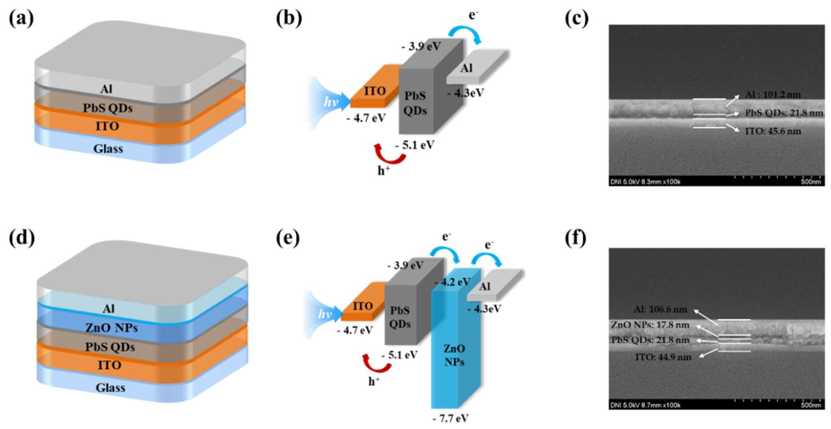
The PbS SWIR sensors were fabricated by spin-coating (LT-MS 200, LTS, Gyeonggi-do, Korea) method on glass substrates coated with a patterned indium tin oxide (ITO) anode. The ITO anode had a thickness of approximately 400 Å and a surface resistance of less than 12 Ω. Initially, to remove contamination on the ITO-patterned glass, the glass was cleaned with acetone, methanol, and deionized water and then exposed to UV ozone (AH-1700, AHTECH LTS Co., Ltd., Gyeonggi-do, Korea) for 15 min. To form the photo active layer, the PbS QDs solution was coated on the substrate, and annealed for 30 min at 110 °C in vacuum oven (ov–11, JEIO Tech, Daejeon Korea). To fabricate the PbS SWIR sensor with ZnO NPs, the ETL was formed by spin-coating ZnO NPs solution and annealed at 90 °C in a vacuum oven for 30 min (when fabricating the sensor without ZnO NPs, this process was omitted). The ETL can effectively transfer the electrons formed in the photoactive layer because of its high electron mobility and appropriate LUMO level of −4.2 eV. Finally, an aluminum (Al) cathode was deposited via thermal evaporation (OLED system, ULTECH, Daegu Korea) in a high-vacuum using a metal shadow mask. The Al electrode was more than 100 nm thick. The emissive area was 9 mm2, as defined by the cross section between the Al cathode and ITO anode. The current–voltage (I–V) characteristics of the PbS SWIR sensors were determined using a parameter analyzer (B1500A, Agilent, Santa Clara, CA, USA). Figure 1 shows the structure, energy band diagrams, and field emission scanning electron microscope (FE-SEM, SU8220, Hitachi, Japan) image of the fabricated sensors. It was confirmed that the thicknesses of the layers of the device without ZnO NPs were ITO: 45.6 nm, PbS QDs: 21.8 nm and Al: 101.2 nm, and those of that using ZnO NPs were ITO: 44.9 nm, PbS QDs: 21.8 nm, ZnO NPs: 17.8 nm and Al: 106.6 nm.
3. Results and Discussion
3.1. Characteristics of Synthesized PbS QDs
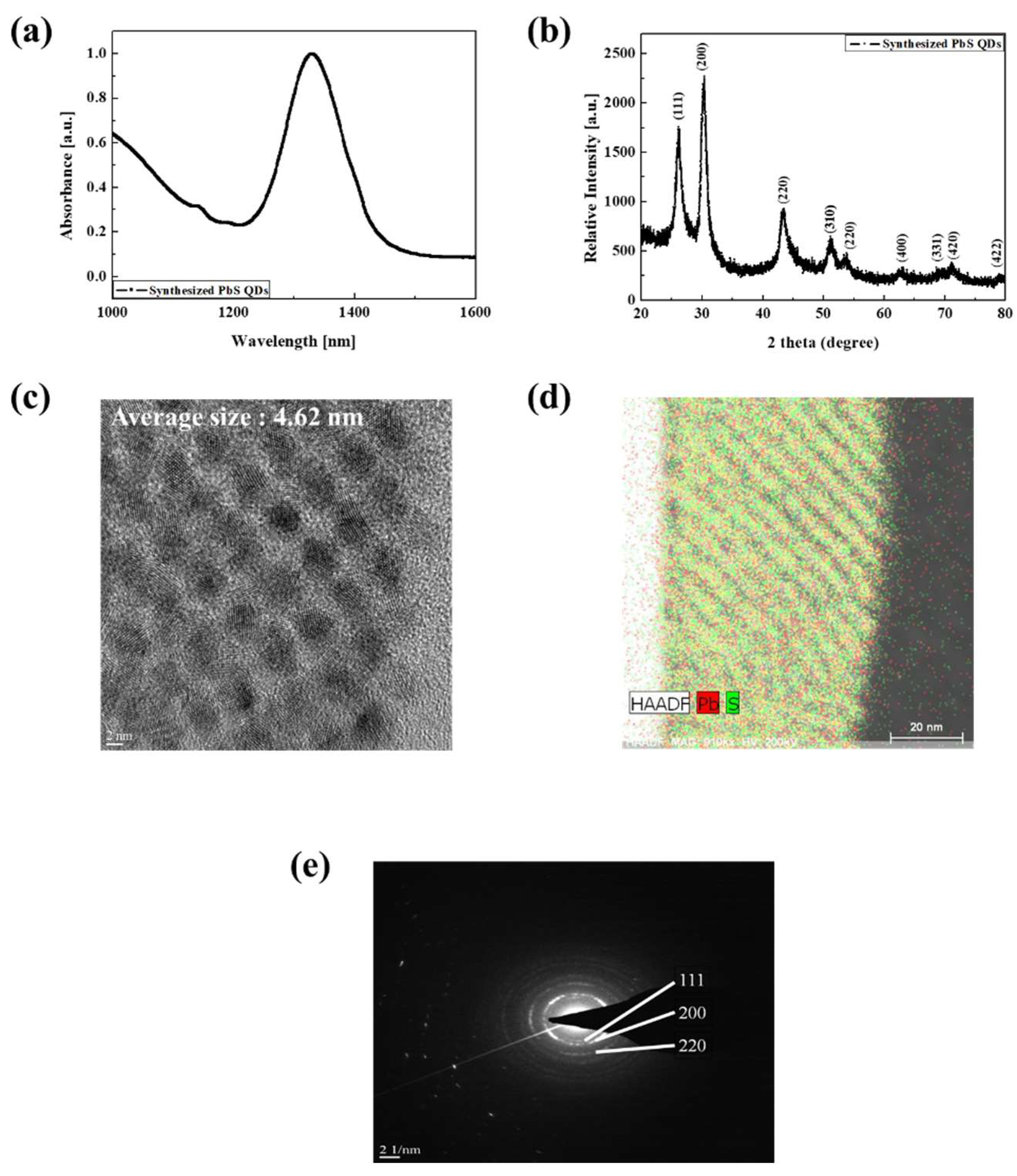
As shown in Figure 2a, we measured the absorption spectra (Cary 5000 UV-Vis-NIR, Agilent, Santa Clara, CA, USA) of the synthesized PbS QDs and confirmed that they have an absorption peak at wavelength λ = 1330 nm. This result means that the synthesized PbS QDs can absorb 1330 nm wavelength light and generate electron-hole pairs (EHPs) when irradiated by an IR light source. To confirm that PbS QDs were indeed synthesized and to compare them with previously reported PbS QDs, X-ray diffraction (XRD, Max-2500, Rigaku, Japan) analysis was performed. The sample for XRD analysis of PbS QDs was formed by spin-coating process on glass substrate (10 mm × 10 mm). As shown in Figure 2b, the XRD result showed the same result as reported, confirming that the PbS QDs were well synthesized [34,35,36]. The following Equation (1) is the Scherrer equation used to calculate the nanocrystal size based on the XRD result and the synthesized PbS QDs calculated.
where K is the shape constant, λ is the wavelength of the X-ray, β is the full width at half maximum (FWHM), and θ is the half value between the incident angle and the scattered X-ray wavelength vector [37,38,39]. We confirmed that their size calculated by Equation (1) was 4.85 nm.
To confirm the formation and composition of the QDs, field-emission transmission electron microscope (FE-TEM, Titan G2 ChemiSTEM Cs Probe, FEI Company, Hillsboro, OR, USA) images were examined. For TEM measurement, the sample was fabricated by spin coating PbS QDs solution on a 10 mm × 10 mm glass substrate and it was cut into 10 μm × 1 μm with width of 70 nm by focused ion beam (FIB, Versa3D LoVac, FEI Company, Hillsboro, OR, USA). From Figure 2c–e, we can see that the synthesized QDs were formed uniformly, and the composition analysis of the TEM image showed that the cores were composed of Pb and S. To determine the size of PbS QDs, we analyzed the TEM image by ImageJ (National Institutes of Health) program, which shows the area of particles in the photograph and calculated their diameter. In the results, 28 PbS QDs of 4 nm to 5 nm were identified and their average size was 4.62 nm, which is similar to the size calculated by the XRD result. The diffraction ring is consistent with the XRD measurement result and confirmed that the PbS QDs has a plane-centered cubic structure [40,41,42].
3.2. Characteristics of Synthesized ZnO NPs
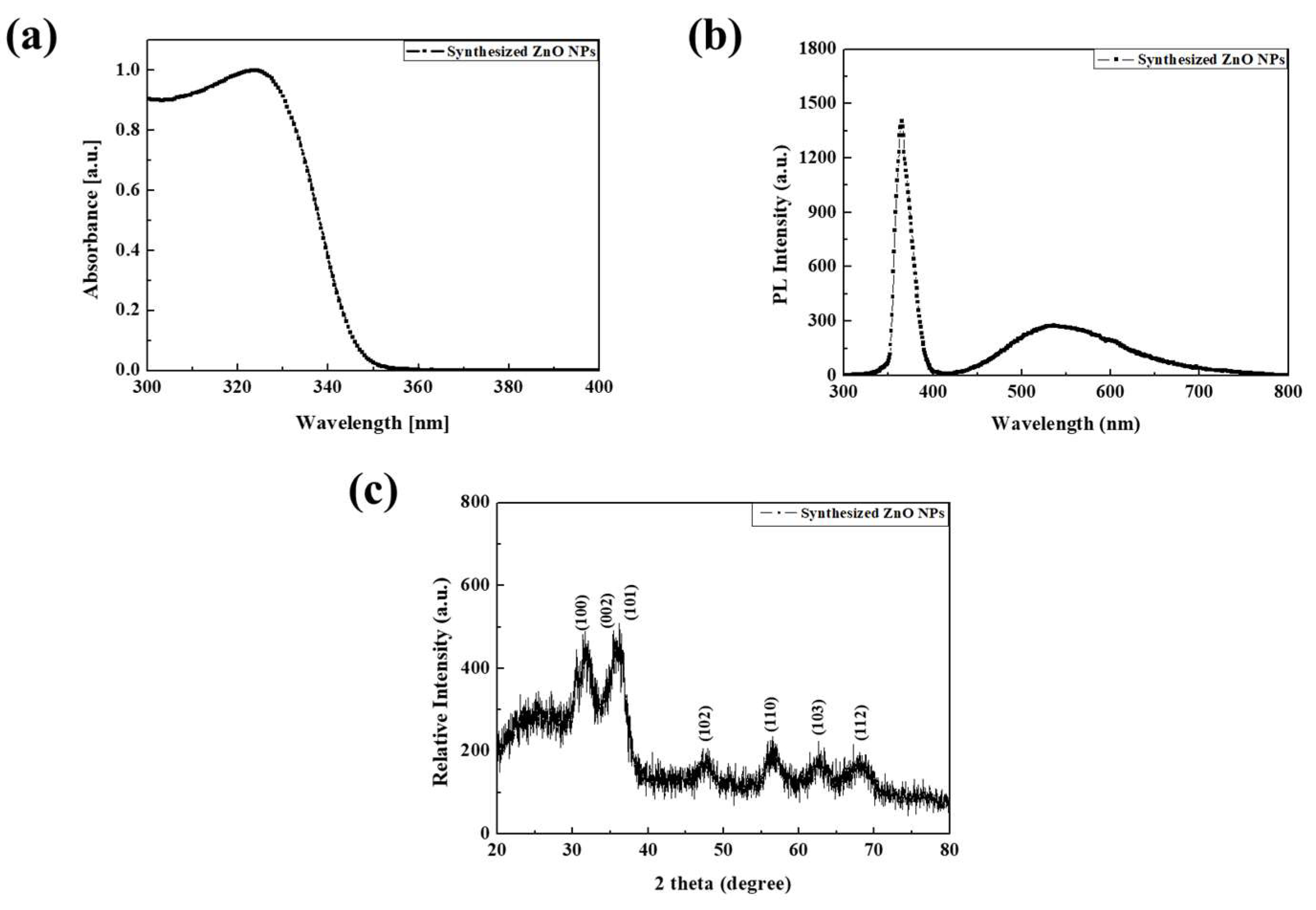
In order to confirm the size and characteristics of the synthesized ZnO NPs, we measured the absorption spectrum (Cary 5000 UV-Vis-NIR, Agilent, Santa Clara, CA, USA), the photoluminescence (PL) characteristics (QE 65000, Ocean optics Inc., Large, FL, USA), and XRD patterns. Figure 3a shows the UV-vis absorption spectra of the ZnO NPs. We confirmed that the synthesized ZnO NPs has a broad absorption band with absorption peak of 323.5 nm in the UV region. Figure 3b shows the PL characteristic of the ZnO NPs has two peaks at 365 nm and 500 nm. The UV radiation, at around 365 nm, originated from the direct bandgap of the ZnO NPs. The other peak, at around 500 nm, originated from the deep trap state on the surface of the ZnO NPs, including oxygen vacancies [43]. To verify the crystal structure, the XRD result of the synthesized ZnO NPs was measured. As shown in Figure 3c, the peak values of the ZnO NPs were measured at 31.7 (100), 34.4 (002), and 36.25 (101), indicating that the synthesized ZnO has a hexagonal wurtzite structure [44,45]. Using the XRD results, the size of the NPs was calculated by the Scherrer Equation (1) to be 4.79 nm.
3.3. Performance of the SWIR Sensors
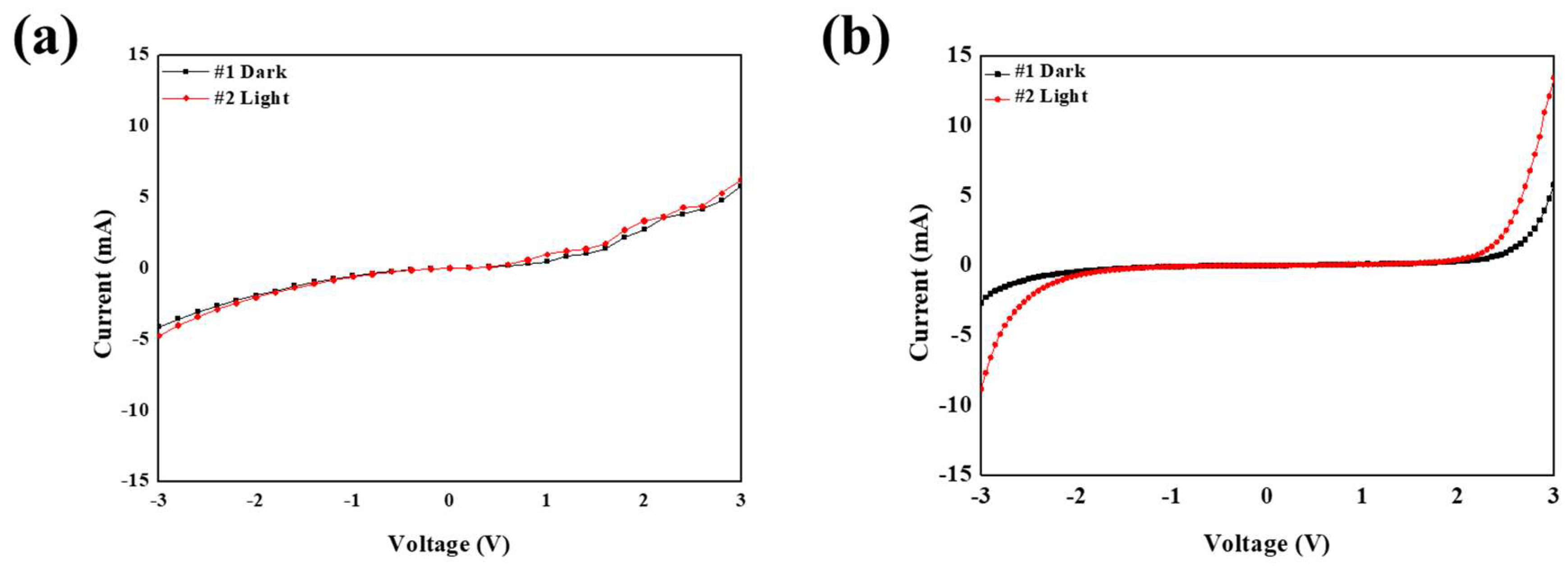
To measure the performance of the fabricated PbS SWIR sensors, the I–V characteristics were measured. When IR light irradiated the PbS SWIR sensor, the EHPs generated at the photo active layer were extracted to the electrodes by the external electric field. The dark current was measured when the IR light source (SL-5, StellarNet, Inc., Tampa, FL, USA) was turned off, and the light current was measured when the IR light source was turned on. The voltage was swept in the range of −3 V to 3 V. Figure 4a,b show the I–V characteristics of the fabricated PbS SWIR sensors. The on/off ratio of the PbS SWIR sensor without ZnO NPs was 1.147 at the maximum current difference, with a dark current of −4.1409 mA and a light current of −4.7533 mA. The on/off ratio of the PbS SWIR sensor with ZnO NPs was 3.293 at the maximum current difference, with a dark current of −2.6899 mA and a light current of −8.8582 mA. In addition, the PbS SWIR sensor with ZnO showed a more stable current characteristic than that without ZnO. As these results show, PbS QDs can detect IR light and ZnO NPs can improve the sensitivity and current stability of the PbS SWIR sensor because of the ZnO NPs’ high electron mobility and proper LUMO level.
4. Conclusions
We synthesized PbS QDs and ZnO NPs to improve the sensitivity and current stability of SWIR sensors. Then, a solution-processed PbS SWIR sensor was fabricated with ZnO NPs and compared to a PbS SWIR sensor without ZnO NPs. The sensor with ZnO NPs had a more sensitive and stable I–V characteristic than the PbS SWIR sensor without ZnO NPs. From measuring the I–V characteristics according to voltage sweep from −3 to 3 V, the on/off ratio of the PbS SWIR sensor with/without ZnO NPs were 1.147, 3.293, respectively, at the maximum current difference. These results confirmed that the on/off ratio of a PbS QDs SWIR sensor using ZnO NPs is 2.871 times higher than that of a PbS SWIR sensor without ZnO NPs. Moreover, the PbS SWIR sensor with ZnO NPs presented a more stable current characteristic than the PbS SWIR sensor without ZnO NPs.
Author Contributions
J.K., S.K. (SaeWan Kim) and J.L. carried out the experiments, collecting the data and drafting the manuscript. J.K., S.K. (SaeWan Kim), O.K., C.P. and B.X. fabricated the devices and performed the measurements. S.K. (ShinWon Kang) and J.B. made significant contributions to the revision of the experiment designs and manuscript editing, guiding the entire study.
Funding
This research received no external funding.
Acknowledgements
This work was supported by a National Research Foundation of Korea (NRF) grant, funded by the Korea Government (MSIP) (No. NRF 2017R1D1A3B03032042) and the BK21 Plus project funded by the Ministry of Education, Korea (21A20131600011) and Samsung Electronics.
Conflicts of Interest
This study has not been published or presented elsewhere in part or in entirety, and is not under consideration for publication by another journal. All the authors have approved of the manuscript and agree with submission to this journal. There are no conflicts of interest to declare.
References
- García de Arquer, F.P.; Armin, A.; Meredith, P.; Sargent, E.H. Solution-processed semiconductors for next-generation photodetectors. Nat. Rev. Mater. 2017, 2, 16100–16115. [Google Scholar] [CrossRef]
- Konstantatos, G.; Howard, I.; Fischer, A.; Hoogland, S.; Clifford, J.; Klem, E.; Levina, L.; Sargent, E.H. Ultrasensitive solution-cast quantum dot photodetectors. Nature 2006, 442, 180–183. [Google Scholar] [CrossRef] [PubMed]
- Michel, E.; Xu, J.; Kim, J.D.; Ferguson, I.; Razeghi, M. InSb infrared photodetectors on Si substrates grown by molecular beam epitaxy. IEEE Photonics Technol. Lett. 1996, 8, 673–675. [Google Scholar] [CrossRef]
- Li, C.; Skidmore, G.D.; Han, C.J. Uncooled VOx Infrared Sensor Development and Application. In Proceedings of the Infrared Technology and Applications XXXVII, Orlando, FL, USA, 25–29 April 2011; SPIE 8012. SPIE: Orlando, FL, USA, 2011. [Google Scholar]
- Li, C.; Han, C.J.; Skidmore, G.D.; Hess, C. DRS uncooled VOx infrared detector development and production status. In Proceedings of the Infrared Technology and Applications XXXVI, Orlando, FL, USA, 5–9 April 2010; SPIE 7660. SPIE: Orlando, FL, USA, 2010. [Google Scholar]
- Graf, M.; Scalari, G.; Hofstetter, D.; Faist, J. Terahertz range quantum well infrared photodetector. Appl. Phys. Lett. 2004, 84, 475–477. [Google Scholar] [CrossRef]
- Wu, W.; Bonakdar, A.; Mohseni, H. Plasmonic enhanced quantum well infrared photodetector with high detectivity. Appl. Phys. Lett. 2010, 96, 161107. [Google Scholar] [CrossRef] [Green Version]
- Liu, H.C.; Li, J.; Thompson, J.R.; Wasilewski, Z.R.; Buchanan, M.; Simmons, JG. Multicolor voltage-tunable quantum-well infrared photodetector. IEEE Electron Device Lett. 1993, 14, 566–568. [Google Scholar] [CrossRef]
- Gunapala, S.D.; Levine, B.F.; Ritter, D.; Hamm, R.; Panish, M.B. InGaAs/InP long wavelength quantum well infrared photodetectors. Appl. Phys. Lett. 1991, 58, 2024–2026. [Google Scholar] [CrossRef]
- Bhattacharya, P.; Su, X.H.; Chakrabarti, S.; Ariyawansa, G.; Perera, A.G.U. Characteristics of a tunneling quantum-dot infrared photodetector operating at room temperature. Appl. Phys. Lett. 2005, 86, 1–3. [Google Scholar] [CrossRef]
- Kim, E.T.; Madhukar, A.; Ye, Z.; Campbell, J.C. High detectivity InAs quantum dot infrared photodetectors. Appl. Phys. Lett. 2004, 84, 3277–3279. [Google Scholar] [CrossRef]
- Qian, L.; Zheng, Y.; Xue, J.; Holloway, P.H. Stable and efficient quantum-dot light-emitting diodes based on solution-processed multilayer structures. Nat. Photonics 2011, 5, 543–548. [Google Scholar] [CrossRef]
- Chuang, C.H.M.; Brown, P.R.; Bulović, V.; Bawendi, M.G. Improved performance and stability in quantum dot solar cells through band alignment engineering. Nat. Mater. 2014, 13, 796–801. [Google Scholar] [CrossRef] [PubMed] [Green Version]
- Hansen, J.A.; Wang, J.; Kawde, A.N.; Xiang, Y.; Gothelf, K.V.; Collins, G. Quantum-dot/aptamer-based ultrasensitive multi-analyte electrochemical biosensor. J. Am. Chem. Soc. 2006, 128, 2228–2229. [Google Scholar] [CrossRef] [PubMed]
- Li, M.; Zhou, D.; Zhao, J.; Zheng, Z.; He, J.; Hu, L.; Xia, Z.; Tang, J.; Liu, H. Resistive gas sensors based on colloidal quantum dot (CQD) solids for hydrogen sulfide detection. Sens. Actuators B Chem. 2015, 217, 198–201. [Google Scholar] [CrossRef]
- Kim, E.; Xia, Y.; Whitesides, G.M. Polymer microstructures formed by moulding in capillaries. Nature 1995, 376, 581–584. [Google Scholar] [CrossRef]
- Liang, R.; Yan, D.; Tian, R.; Yu, X.; Shi, W.; Li, C.; Wei, M.; Evans, G.D.; Duan, X. Quantum dots-based flexible films and their application as the phosphor in white light-emitting diodes. Chem. Mater. 2014, 26, 2595–2600. [Google Scholar] [CrossRef]
- Tanabe, K.; Watanabe, K.; Arakawa, Y. Flexible thin-film InAs/GaAs quantum dot solar cells. Appl. Phys. Lett. 2012, 100, 2–6. [Google Scholar] [CrossRef]
- Liu, H.; Li, M.; Voznyy, O.; Hu, L.; Fu, Q.; Zhou, D.; Xia, Z.; Sargent, E.H.; Tang, J. Physically flexible, rapid-response gas sensor based on colloidal quantum dot solids. Adv. Mater. 2014, 26, 2718–2724. [Google Scholar] [CrossRef]
- Hines, M.A.; Scholes, G.D. Colloidal PbS nanocrystals with size-tunable near-infrared emission: Observation of post-synthesis self-narrowing of the particle size distribution. Adv. Mater. 2003, 15, 1844–1849. [Google Scholar] [CrossRef]
- Moreels, I.; Justo, Y.; De Geyter, B.; Haustraete, K.; Martins, J.C.; Hens, Z. Size-tunable, bright, and stable PbS quantum dots: A surface chemistry study. ACS Nano 2011, 5, 2004–2012. [Google Scholar] [CrossRef]
- Kim, J.S.; Kang, B.H.; Jeong, H.M.; Kim, S.W.; Xu, B.; Kang, S.W. Quantum dot light emitting diodes using size-controlled ZnO NPs. Curr. Appl. Phys. 2018, 18, 681–685. [Google Scholar] [CrossRef]
- Kahn, M.L.; Monge, M.; Collière, V.; Senocq, F.; Maisonnat, A.; Chaudret, B. Size- and shape-control of crystalline zinc oxide nanoparticles: A new organometallic synthetic method. Adv. Funct. Mater. 2005, 15, 458–468. [Google Scholar] [CrossRef]
- Spanhel, L. Colloidal ZnO nanostructures and functional coatings: A survey. J. Sol-Gel Sci. Technol. 2006, 39, 7–24. [Google Scholar] [CrossRef]
- Moreels, I.; Lambert, K.; Smeets, D.; Muynck, D.; Nollet, T.; Martins, J.; Vanhaecke, F.; Vantomme, A.; Delerue, C.; Allan, G.; et al. Size-dependent optical properties of colloidal PbS quantum dots. ACS Nano 2009, 3, 3023–3030. [Google Scholar] [CrossRef] [PubMed]
- Zhao, H.; Chaker, M.; Wu, N.; Ma, D. Towards controlled synthesis and better understanding of highly luminescent PbS/CdS core/shell quantum dots. J. Mater. Chem. 2011, 21, 8898–8904. [Google Scholar] [CrossRef]
- Sargent, E.H. Size-tunable infrared (1000–1600 nm) electroluminescence from solution-processible PbS quantum dot nanocrystals: Towards monolithic optoelectronic integration on silicon. J. Mod. Opt. 2004, 51, 2797–2803. [Google Scholar]
- Yang, X.; Ren, F.; Wang, Y.; Ding, T.; Sun, H.; Ma, D.; Sun, X.W. Iodide capped PbS/CdS core-shell quantum dots for efficient long-wavelength near-infrared light-emitting diodes. Sci. Rep. 2017, 7, 14741–14746. [Google Scholar] [CrossRef]
- Nam, M.W.; Lee, T.Y.; Kim, S.W.; Kim, S.W.; Kim, S.W.; Lee, K.K. Two strategies to enhance efficiency of PbS quantum dot solar cells: Removing surface organic ligands and configuring a bilayer heterojunction with a new conjugated polymer. Org. Electron. Phys. Mater. Appl. 2014, 15, 391–398. [Google Scholar] [CrossRef]
- Nam, M.W.; Park, J.P.; Kim, S.W.; Lee, K.K. Broadband-absorbing hybrid solar cells with efficiency greater than 3% based on a bulk heterojunction of PbS quantum dots and a low-bandgap polymer. J. Mater. Chem. A 2014, 2, 3978–3985. [Google Scholar] [CrossRef]
- Lin, K.F.; Cheng, H.M.; Hsu, H.C.; Lin, L.J.; Hsieh, W.F. Band gap variation of size-controlled ZnO quantum dots synthesized by sol-gel method. Chem. Phys. Lett. 2005, 409, 208–211. [Google Scholar] [CrossRef]
- Kim, O.S.; Kang, B.H.; Lee, J.S.; Lee, S.W.; Cha, S.H.; Lee, J.W.; Kim, S.W.; Kim, S.H.; Kang, S.W. Efficient quantum dots light-emitting devices using polyvinyl pyrrolidone-capped zno nanoparticles with enhanced charge transport. IEEE Electron Device Lett. 2016, 37, 1022–1024. [Google Scholar] [CrossRef]
- Sun, D.; Wong, M.; Sun, L.; Li, Y.; Miyatake, N.; Sue, H.J. Purification and stabilization of colloidal ZnO nanoparticles in methanol. J. Sol-Gel Sci. Technol. 2007, 43, 237–243. [Google Scholar] [CrossRef]
- Maulu, A.; Rodríguez-Cantó, P.J.; Navarro-Arenas, J.; Abargues, R.; Sanchez-Royo, J.F.; Garcia-Calzada, R.; Martinez-Pastor, J.P. Strongly-coupled PbS QD solids by doctor blading for IR photodetection. RSC Adv. 2016, 6, 80201–80212. [Google Scholar] [CrossRef]
- Zhang, D.; Song, J.; Zhang, J.; Wang, Y.; Zhang, S.; Miao, X. A facile and rapid synthesis of lead sulfide colloidal quantum dots using in situ generated H2S as the sulfur source. CrystEngComm 2013, 15, 2532–2536. [Google Scholar] [CrossRef]
- Mote, V.; Purushotham, Y.; Dole, B. Williamson-Hall analysis in estimation of lattice strain in nanometer-sized ZnO particles. J. Appl. Phys. 2012, 6, 2–9. [Google Scholar] [CrossRef]
- Gao, J.; Jeong, S.H.; Lin, F.; Erslev, P.T.; Semonin, O.E.; Luther, J.M.; Beard, M.C. Improvement in carrier transport properties by mild thermal annealing of PbS quantum dot solar cells. Appl. Phys. Lett. 2013, 102, 43506–43510. [Google Scholar] [CrossRef]
- Zhong, X.; Liu, S.; Zhang, Z.; Li, L.; Wei, Z.; Knoll, W. Synthesis of high-quality CdS, ZnS, and ZnxCd1−xS nanocrystals using metal salts and elemental sulfur. J. Mater. Chem. 2004, 14, 2790–2794. [Google Scholar] [CrossRef]
- Pacholski, C.; Kornowski, A.; Weller, H. Self-assembly of ZnO: from nanodots to nanorods. Angew. Chem. Int. Ed. 2002, 41, 1188–1191. [Google Scholar] [CrossRef]
- Cademartiri, L.; Montanari, E.; Calestani, G.; Migliori, A.; Guagliardi, A.; Ozin, G.A. Size-Dependent Extinction Coefficients of PbS Quantum Dots. J. Am. Chem. Soc. 2006, 128, 10337–10346. [Google Scholar] [CrossRef]
- Bakueva, L.; Gorelikov, I.; Musikhin, S.; Zhao, X.S.; Sargent, E.H.; Kumacheva, E. PbS Quantum Dots with Stable Efficient Luminescence in the near-IR Spectral Range. Adv. Mater. 2004, 16, 926–929. [Google Scholar] [CrossRef]
- Zeng, X.; Gao, H.; Pan, D.; Sun, Y.; Cao, j.; Wu, Z.; Pan, Z. Highly sensitive electrochemical determination of alfatoxin B1 using quantum dots-assembled amplification labels. Sensors 2015, 15, 20648–20658. [Google Scholar] [CrossRef]
- Seow, Z.L.S.; Wong, A.S.W.; Thavasi, V.; Jose, R.; Ramakrishna, S.; Ho, G.W. Controlled synthesis and application of ZnO nanoparticles, nanorods and nanospheres in dye-sensitized solar cells. Nanotechnology 2009, 20, 45604–45609. [Google Scholar] [CrossRef] [PubMed]
- Lee, S.; Jeong, S.H.; Kim, D.J.; Hwang, S.H.; Jeon, M.H.; Moon, J.H. ZnO nanoparticles with controlled shapes and sizes prepared using a simple polyol synthesis. Superlattices Microstruct. 2008, 43, 330–339. [Google Scholar] [CrossRef]
- Djurišić, A.B.; Choy, W.C.H.; Roy, V.A.L.; Leung, Y.H.; Kwong, C.Y.; Cheah, K.W.; Rao, T.K.G.; Chan, W.K.; Lui, H.F.; Surya, C. Photoluminescence and electron paramagnetic resonance of ZnO tetrapod structures. Adv. Funct. Mater. 2004, 14, 856–864. [Google Scholar] [CrossRef]
Figure 1.
(a) Schematic device structure, (b) energy band diagram and (c) FE-SEM image of the PbS SWIR sensor without ZnO NPs, (d) schematic representation of the device structure, (e) energy band diagram and (f) FE-SEM image of the PbS SWIR sensor with ZnO NPs.
Figure 1.
(a) Schematic device structure, (b) energy band diagram and (c) FE-SEM image of the PbS SWIR sensor without ZnO NPs, (d) schematic representation of the device structure, (e) energy band diagram and (f) FE-SEM image of the PbS SWIR sensor with ZnO NPs.

Figure 2.
(a) Absorbance property, (b) XRD analysis, (c) TEM image, (d) composition analysis, and (e) diffraction ring of the synthesized PbS QDs.
Figure 2.
(a) Absorbance property, (b) XRD analysis, (c) TEM image, (d) composition analysis, and (e) diffraction ring of the synthesized PbS QDs.

Figure 3.
(a) Absorbance property, (b) PL characteristic and (c) XRD analysis of the synthesized ZnO NPs.
Figure 3.
(a) Absorbance property, (b) PL characteristic and (c) XRD analysis of the synthesized ZnO NPs.

Figure 4.
I–V characteristics of (a) PbS SWIR sensor without ZnO NPs, and (b) PbS SWIR sensor with ZnO NPs.
Figure 4.
I–V characteristics of (a) PbS SWIR sensor without ZnO NPs, and (b) PbS SWIR sensor with ZnO NPs.

© 2019 by the authors. Licensee MDPI, Basel, Switzerland. This article is an open access article distributed under the terms and conditions of the Creative Commons Attribution (CC BY) license (http://creativecommons.org/licenses/by/4.0/).
Share and Cite
MDPI and ACS Style
Kwon, J.; Kim, S.; Lee, J.; Park, C.; Kim, O.; Xu, B.; Bae, J.; Kang, S. Uncooled Short-Wave Infrared Sensor Based on PbS Quantum Dots Using ZnO NPs. Nanomaterials 2019, 9, 926. https://doi.org/10.3390/nano9070926
AMA Style
Kwon J, Kim S, Lee J, Park C, Kim O, Xu B, Bae J, Kang S. Uncooled Short-Wave Infrared Sensor Based on PbS Quantum Dots Using ZnO NPs. Nanomaterials. 2019; 9(7):926. https://doi.org/10.3390/nano9070926
Chicago/Turabian StyleKwon, JinBeom, SaeWan Kim, JaeSung Lee, CheolEon Park, OkSik Kim, Binrui Xu, JinHyuk Bae, and ShinWon Kang. 2019. "Uncooled Short-Wave Infrared Sensor Based on PbS Quantum Dots Using ZnO NPs" Nanomaterials 9, no. 7: 926. https://doi.org/10.3390/nano9070926
Note that from the first issue of 2016, this journal uses article numbers instead of page numbers. See further details here.