Metalenses Based on Symmetric Slab Waveguide and c-TiO2: Efficient Polarization-Insensitive Focusing at Visible Wavelengths


 ,
, 
Abstract
:
1. Introduction
2. Methods
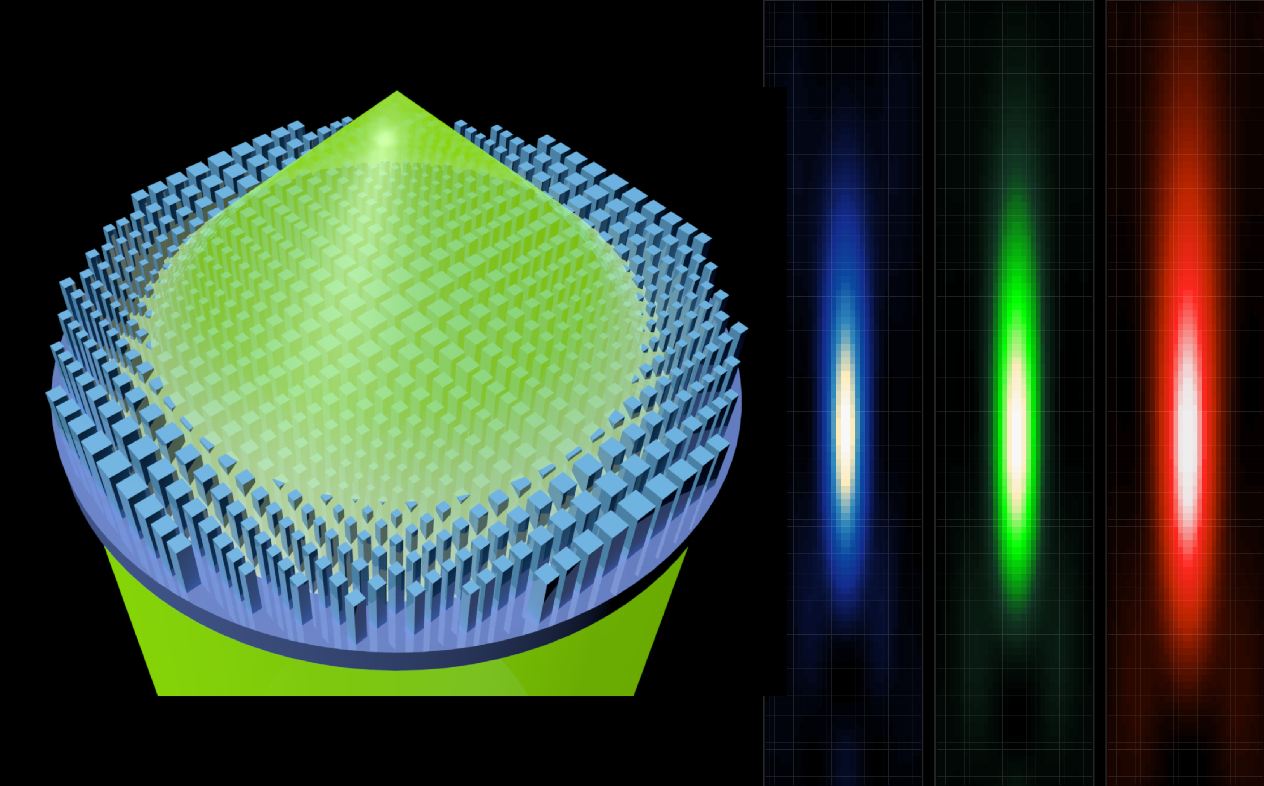
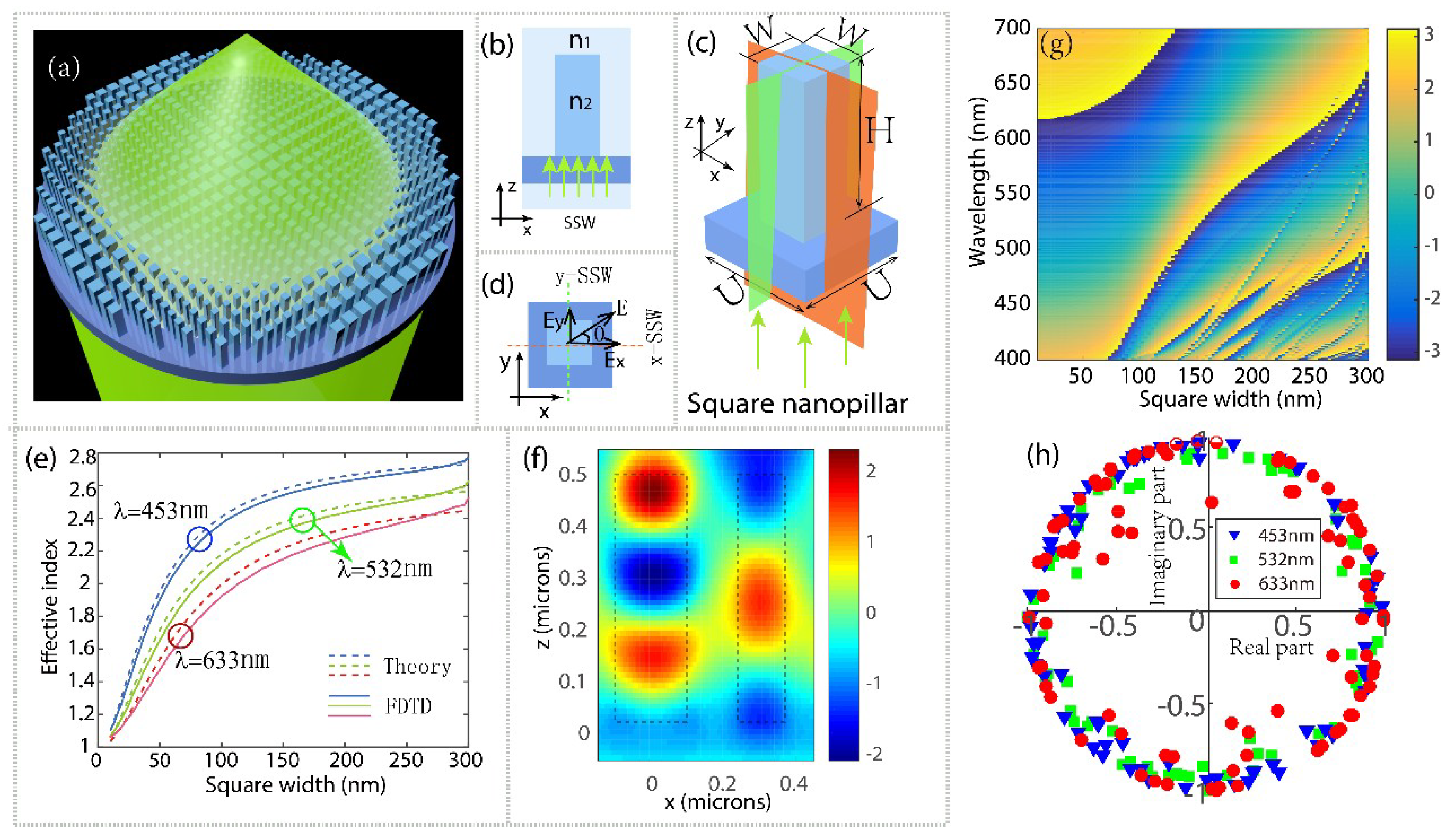
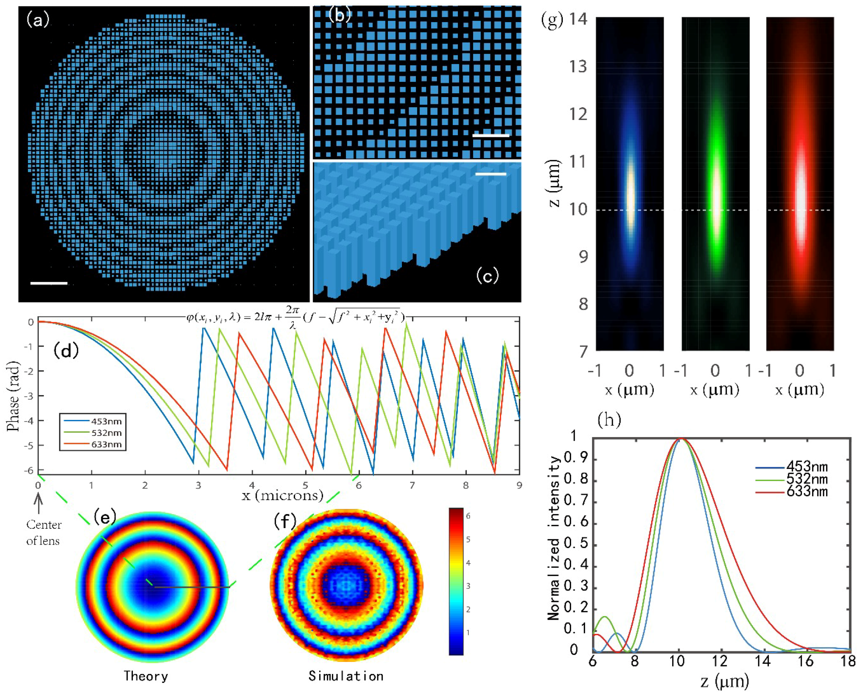
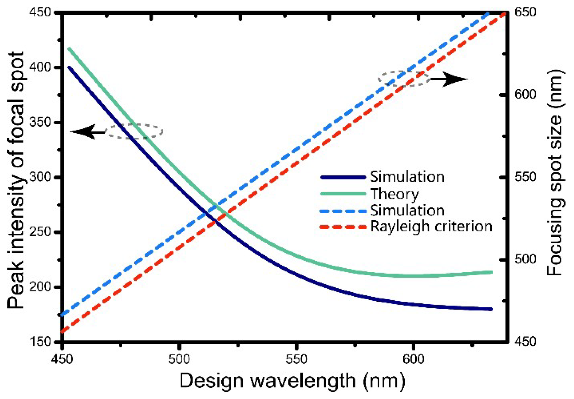
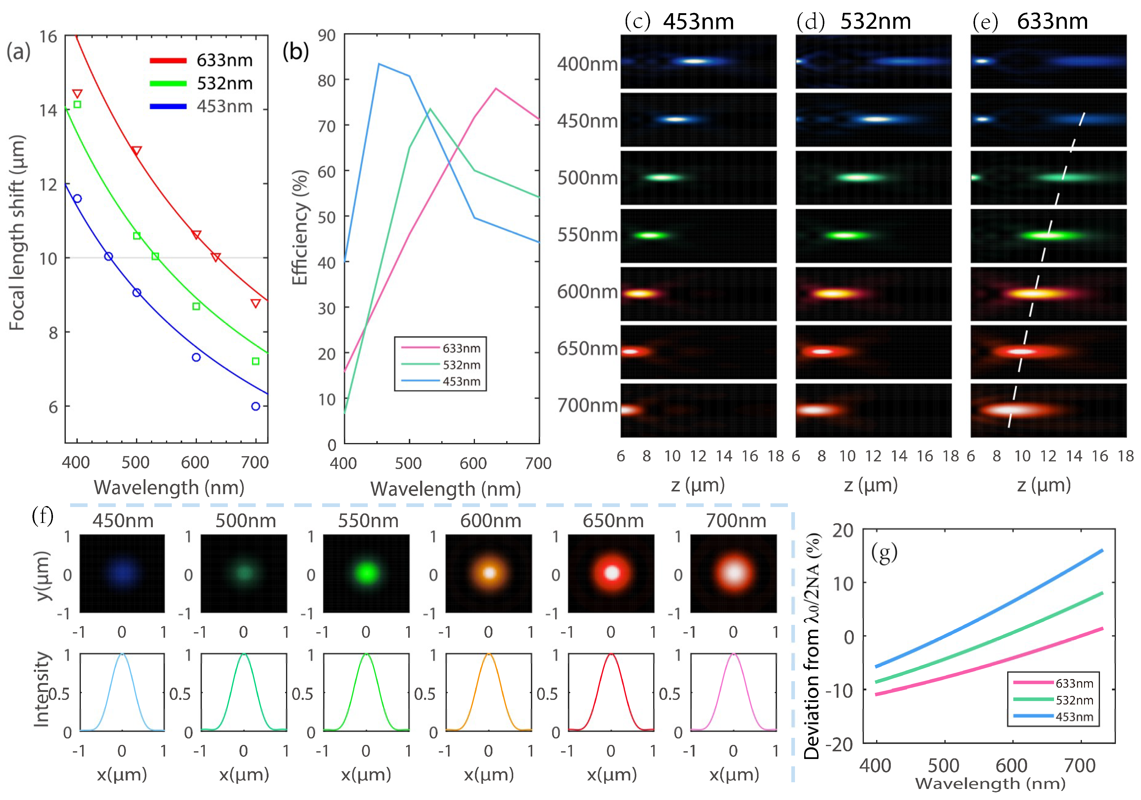
3. Results
4. Discussions
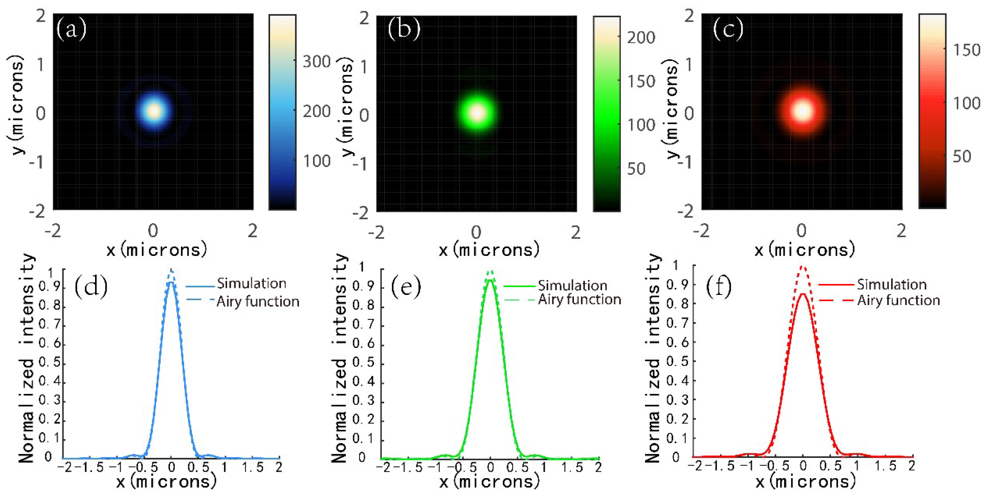
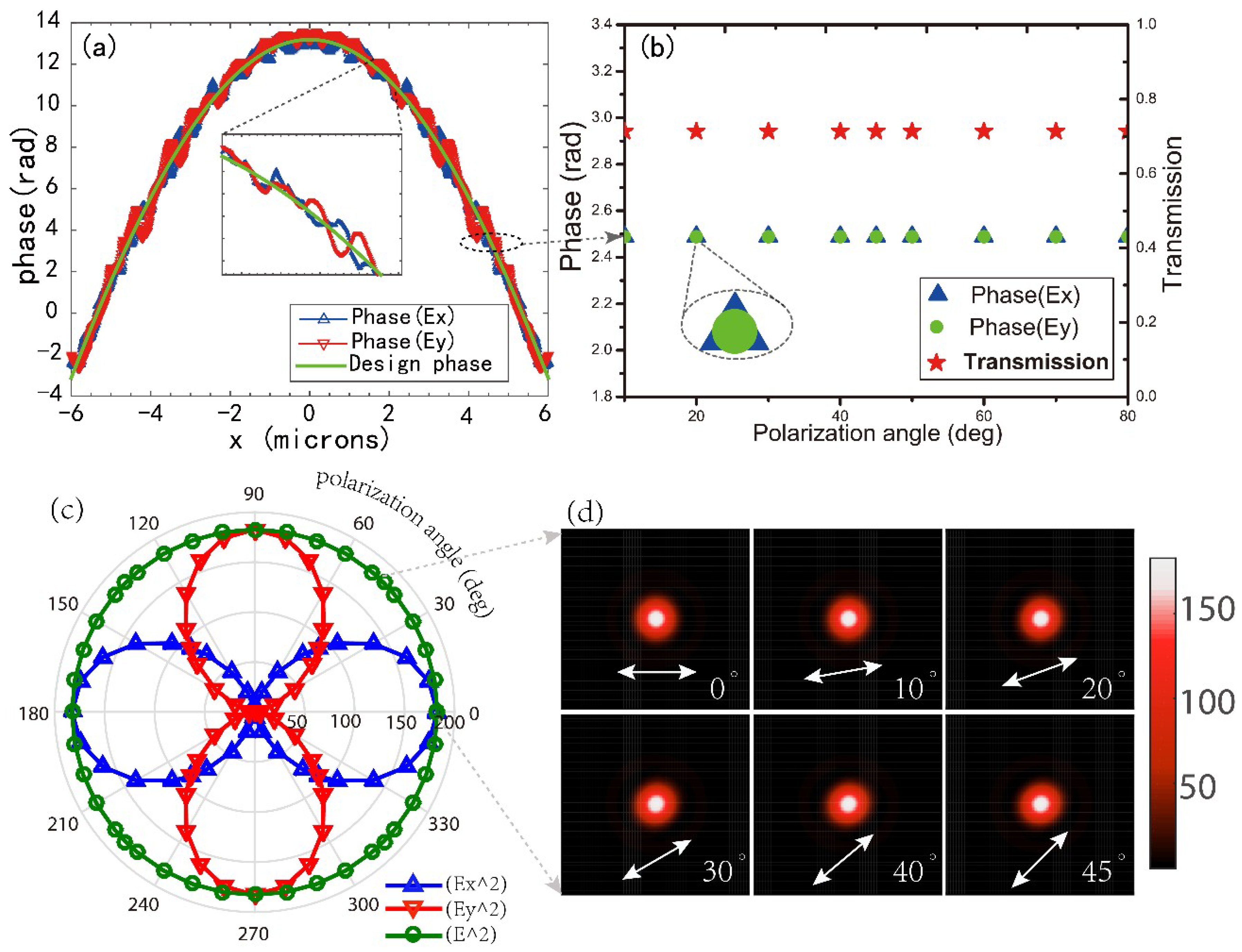
4.1. Characterization of Aberration
4.2. Polarization-Insensitive Properties
4.3. Comparision of Previously Reported Metalenses and Our Work
5. Conclusions
Supplementary Materials
Author Contributions
Funding
Acknowledgments
Conflicts of Interest
References
- Kildishev, A.V.; Boltasseva, A.; Shalaev, V.M. Planar photonics with metasurfaces. Science 2013, 339, 1232009. [Google Scholar] [CrossRef] [PubMed]
- Arbabi, A.; Horie, Y.; Ball, A.J.; Bagheri, M.; Faraon, A. Subwavelength-thick lenses with high numerical apertures and large efficiency based on high-contrast transmitarrays. Nat. Commun. 2015, 6, 7069. [Google Scholar] [CrossRef] [PubMed] [Green Version]
- Khorasaninejad, M.; Aieta, F.; Kanhaiya, P.; Kats, M.A.; Genevet, P.; Rousso, D.; Capasso, F. Achromatic metasurface lens at telecommunication wavelengths. Nano Lett. 2015, 15, 5358–5362. [Google Scholar] [CrossRef] [PubMed]
- Wang, W.; Guo, Z.; Li, R.; Zhang, J.; Li, Y.; Wang, X.; Qu, S. Plasmonics metalens independent from the incident polarizations. Opt. Express 2015, 23, 16782–16791. [Google Scholar] [CrossRef] [PubMed]
- Aieta, F.; Genevet, P.; Kats, M.A.; Yu, N.; Blanchard, R.; Gaburro, Z.; Capasso, F. Aberration-free ultrathin flat lenses and axicons at telecom wavelengths based on plasmonic metasurfaces. Nano Lett. 2012, 12, 4932–4936. [Google Scholar] [CrossRef] [PubMed]
- Chen, W.T.; Khorasaninejad, M.; Zhu, A.Y.; Oh, J.; Devlin, R.C.; Zaidi, A.; Capasso, F. Generation of wavelength-independent subwavelength Bessel beams using metasurfaces. Light-Sci. Appl. 2017, 6, e16259. [Google Scholar] [CrossRef] [PubMed]
- Yu, N.; Aieta, F.; Genevet, P.; Kats, M.A.; Gaburro, Z.; Capasso, F. A broadband, background-free quarter-wave plate based on plasmonic metasurfaces. Nano Lett. 2012, 12, 6328–6333. [Google Scholar] [CrossRef] [PubMed]
- Wang, D.; Gu, Y.; Gong, Y.; Qiu, C.W.; Hong, M. An ultrathin terahertz quarter-wave plate using planar babinet-inverted metasurface. Opt. Express 2015, 23, 11114–11122. [Google Scholar] [CrossRef] [PubMed]
- Ma, X.; Pu, M.; Li, X.; Huang, C.; Wang, Y.; Pan, W.; Zhao, B.; Cui, J.; Wang, C.; Zhao, Z.; et al. A planar chiral meta-surface for optical vortex generation and focusing. Sci. Rep. 2015, 5, 10365. [Google Scholar] [CrossRef] [PubMed] [Green Version]
- Sun, S.; Yang, K.Y.; Wang, C.M.; Juan, T.K.; Chen, W.T.; Liao, C.Y.; He, Q.; Xiao, S.; Kung, W.-T.; Guo, G.-Y.; et al. High-efficiency broadband anomalous reflection by gradient meta-surfaces. Nano Lett. 2012, 12, 6223–6229. [Google Scholar] [CrossRef] [PubMed]
- Larouche, S.; Tsai, Y.-J.; Tyler, T.; Jokerst, N.M.; Smith, D.R. Infrared metamaterial phase holograms. Nat. Mater. 2012, 11, 450. [Google Scholar] [CrossRef] [PubMed]
- Rogers, E.T.F.; Lindberg, J.; Roy, T.; Savo, S.; Chad, J.E.; Dennis, M.R.; Zheludev, N.I. A super-oscillatory lens optical microscope for subwavelength imaging. Nat. Mater. 2012, 11, 432. [Google Scholar] [CrossRef] [PubMed]
- Pors, A.; Nielsen, M.G.; Eriksen, R.L.; Bozhevolnyi, S.I. Broadband focusing flat mirrors based on plasmonic gradient metasurfaces. Nano Lett. 2013, 13, 829–834. [Google Scholar] [CrossRef] [PubMed]
- Saeidi, C.; Weide, D. Wideband plasmonic focusing metasurfaces. Appl. Phys. Lett. 2014, 105, 053107. [Google Scholar] [CrossRef]
- Chen, W.T.; Yang, K.-Y.; Wang, C.-M.; Huang, Y.-W.; Sun, G.; Chiang, I.-D.; Liao, C.Y.; Hsu, W.-L.; Lin, H.T.; Sun, S.; et al. High-efficiency broadband meta-hologram with polarization-controlled dual images. Nano Lett. 2014, 14, 225–230. [Google Scholar] [CrossRef] [PubMed]
- Zheng, G.; Mühlenbernd, H.; Kenney, M.; Li, G.; Zentgraf, T.; Zhang, S. Metasurface holograms reaching 80% efficiency. Nat. Nanotechnol. 2015, 10, 308. [Google Scholar] [CrossRef] [PubMed]
- Khorasaninejad, M.; Crozier, K.B. Silicon nanofin grating as a miniature chirality-distinguishing beam-splitter. Nat. Commun. 2014, 5, 5386. [Google Scholar] [CrossRef] [PubMed] [Green Version]
- Chong, K.E.; Staude, I.; James, A.; Dominguez, J.; Liu, S.; Campione, S.; Subramania, G.S.; Luk, T.S.; Decker, M.; Neshev, D.N.; et al. Polarization-independent silicon metadevices for efficient optical wavefront control. Nano Lett. 2015, 15, 5369–5374. [Google Scholar] [CrossRef] [PubMed]
- Jahani, S.; Jacob, Z. All-dielectric metamaterials. Nat. Nanotechnol. 2016, 11, 23. [Google Scholar] [CrossRef] [PubMed]
- Zhan, A.; Colburn, S.; Trivedi, R.; Fryett, T.K.; Dodson, C.M.; Majumdar, A. Low-contrast dielectric metasurface optics. ACS Photonics 2016, 3, 209–214. [Google Scholar] [CrossRef]
- Wang, S.; Wu, P.C.; Su, V.C.; Lai, Y.C.; Chen, M.K.; Kuo, H.Y.; Chen, B.H.; Chen, Y.H.; Huang, T.-T.; Wang, J.H.; et al. A broadband achromatic metalens in the visible. Nat. Nanotechnol. 2018, 13, 227–232. [Google Scholar] [CrossRef] [PubMed]
- Chen, B.H; Wu, P.C; Su, V.C; Lai, Y.C; Chu, C.H; Lee, C.; Chen, J.-W.; Chen, Y.H.; Lan, Y.-C.; Kuan, C.-H.; et al. GaN metalens for pixel-level full-color routing at visible light. Nano Lett. 2017, 17, 6345–6352. [Google Scholar] [CrossRef] [PubMed]
- Khorasaninejad, M.; Chen, W.T; Devlin, R.C; Oh, J.; Zhu, A.Y.; Capasso, F. Metalenses at visible wavelengths: Diffraction-limited focusing and subwavelength resolution imaging. Science 2016, 352, 1190–1194. [Google Scholar] [CrossRef] [PubMed]
- Khorasaninejad, M.; Shi, Z.; Zhu, A.Y.; Chen, W.T.; Sanjeev, V.; Zaidi, A.; Capasso, F. Achromatic metalens over 60 nm bandwidth in the visible and metalens with reverse chromatic dispersion. Nano Lett. 2017, 17, 1819–1824. [Google Scholar] [CrossRef] [PubMed]
- Chen, W.T.; Zhu, A.Y.; Khorasaninejad, M.; Shi, Z.; Sanjeev, V.; Capasso, F. Immersion meta-lenses at visible wavelengths for nanoscale imaging. Nano Lett. 2017, 17, 3188–3194. [Google Scholar] [CrossRef] [PubMed]
- Chen, W.T.; Zhu, A.Y.; Sanjeev, V.; Khorasaninejad, M.; Shi, Z.; Lee, E.; Capasso, F. A broadband achromatic metalens for focusing and imaging in the visible. Nat. Nanotechnol. 2018, 13, 220–226. [Google Scholar] [CrossRef] [PubMed] [Green Version]
- Khorasaninejad, M.; Chen, W.T.; Zhu, A.Y.; Oh, J.; Devlin, R.C.; Rousso, D.; Capasso, F. Multispectral chiral imaging with a metalens. Nano Lett. 2016, 16, 4595–4600. [Google Scholar] [CrossRef] [PubMed]
- Bomzon, Z.; Biener, G.; Kleiner, V.; Hasman, E. Space-variant pancharatnam–berry phase optical elements with computer-generated subwavelength gratings. Opt. Lett. 2002, 27, 1141. [Google Scholar] [CrossRef] [PubMed]
- Khorasaninejad, M.; Zhu, A.Y.; Roques-Carmes, C.; Chen, W.T.; Oh, J.; Mishra, I.; Devlin, R.C.; Capasso, F. Polarization-insensitive metalenses at visible wavelengths. Nano Lett. 2016, 16, 7229–7234. [Google Scholar] [CrossRef] [PubMed]
- Kang, M.; Feng, T.; Wang, H.T.; Li, J. Wave front engineering from an array of thin aperture antennas. Opt. Express 2012, 20, 15882–15890. [Google Scholar] [CrossRef] [PubMed]
- Ding, X.; Monticone, F.; Zhang, K.; Zhang, L.; Gao, D.; Burokor, S.N.; Lustrac, A.; Wu, Q.; Qiu, C.; Aiu, A. Ultrathin Pancharatnam–Berry metasurface with maximal cross-polarization efficiency. Adv. Mater. 2015, 27, 1195–1200. [Google Scholar] [CrossRef] [PubMed]
- Guo, Z.; Zhu, L.; Shen, F.; Zhou, H.; Gao, R. Dielectric metasurface based high-efficiency polarization splitters. RSC Adv. 2017, 7, 9872–9879. [Google Scholar] [CrossRef]
- Liang, Y.; Liu, H.; Wang, F.; Meng, H.; Guo, J.; Li, J.; Wei, Z. High-efficiency, near-diffraction limited, dielectric metasurface lenses based on crystalline titanium dioxide at visible wavelengths. Nanomaterials 2018, 8, 288. [Google Scholar] [CrossRef] [PubMed]
- Zhu, Y.; Yuan, W.; Sun, H.; Yu, Y. Broadband ultra-deep sub-diffraction-limit optical focusing by metallic graded-index (MGRIN) lenses. Nanomaterials 2017, 7, 221. [Google Scholar] [CrossRef] [PubMed]
- Jiang, X.Y.; Ye, J.S.; He, J.W.; Wang, X.K.; Hu, D.; Feng, S.F.; Kan, Q.; Zhang, Y. An ultrathin terahertz lens with axial long focal depth based on metasurfaces. Opt. Express 2013, 21, 30030–30038. [Google Scholar] [CrossRef] [PubMed]
- Jia, D.; Tian, Y.; Ma, W.; Gong, X.; Yu, J.; Zhao, G.; Yu, X. Transmissive terahertz metalens with full phase control based on a dielectric metasurface. Opt. Lett. 2017, 42, 4494–4497. [Google Scholar] [CrossRef] [PubMed]
- Yariv, A.; Yeh, P. Photonics: Optical Electronics in Modern Communications, 6th ed.; The Oxford Series in Electrical and Computer Engineering; Oxford University Press: New York, NY, USA, 2007. [Google Scholar]
- Khorasaninejad, M.; Capasso, F. Broadband multifunctional efficient meta-gratings based on dielectric waveguide phase shifters. Nano Lett. 2015, 15, 6709–6715. [Google Scholar] [CrossRef] [PubMed]
- Lalanne, P. Waveguiding in blazed-binary diffractive elements. J. Opt. Soc. Am. A 1999, 16, 2517. [Google Scholar] [CrossRef] [Green Version]
- Ni, X.; Ishii, S.; Kildishev, A.V.; Shalaev, V.M. Ultra-thin, planar, Babinet-inverted plasmonic metalenses. Light Sci. Appl. 2013, 2, e72. [Google Scholar] [CrossRef]


| Reference | Phase Mechanism | Materials | λ(nm) | Polarization | Thickness(nm) | Efficiency |
|---|---|---|---|---|---|---|
| Aieta et al. [5] | Resonance tuning | Au | 1550 | Linear (cross *) | 60 | 1% |
| Ni et al. [40] | Resonance tuning | Au | 676 | Linear (cross *) | 30 | 10% |
| Mo et al. [23] | P-B | a-TiO2 | 405, 532, 660 | Circular (cross *) | 600 | 86%, 73%, 66% |
| Shu et al. [21] | P-B | GaN | 530 | Circular (cross *) | 800 | 67% |
| This work | Slab Waveguide | c-TiO2 | 453, 532, 633 | Insensitive | 488 | 83.4%, 73.5%, 78% |
| Mo et al. [29] | Circular Waveguide | a-TiO2 | 405, 532, 660 | Insensitive | 400, 600 | 30%, 70%, 90% |
© 2018 by the authors. Licensee MDPI, Basel, Switzerland. This article is an open access article distributed under the terms and conditions of the Creative Commons Attribution (CC BY) license (http://creativecommons.org/licenses/by/4.0/).
Share and Cite
Liang, Y.; Wei, Z.; Guo, J.; Wang, F.; Meng, H.; Liu, H. Metalenses Based on Symmetric Slab Waveguide and c-TiO2: Efficient Polarization-Insensitive Focusing at Visible Wavelengths. Nanomaterials 2018, 8, 699. https://doi.org/10.3390/nano8090699
Liang Y, Wei Z, Guo J, Wang F, Meng H, Liu H. Metalenses Based on Symmetric Slab Waveguide and c-TiO2: Efficient Polarization-Insensitive Focusing at Visible Wavelengths. Nanomaterials. 2018; 8(9):699. https://doi.org/10.3390/nano8090699
Chicago/Turabian StyleLiang, Yaoyao, Zhongchao Wei, Jianping Guo, Faqiang Wang, Hongyun Meng, and Hongzhan Liu. 2018. "Metalenses Based on Symmetric Slab Waveguide and c-TiO2: Efficient Polarization-Insensitive Focusing at Visible Wavelengths" Nanomaterials 8, no. 9: 699. https://doi.org/10.3390/nano8090699