
Homogeneous Spatial Distribution of Deuterium Chemisorbed on Free-Standing Graphene

 , , , , , , ,
  ,
,  , , and
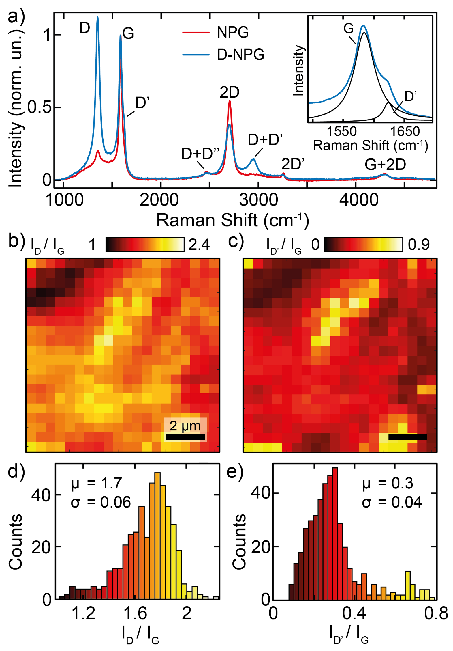
Abstract
:1. Introduction
2. Materials and Methods
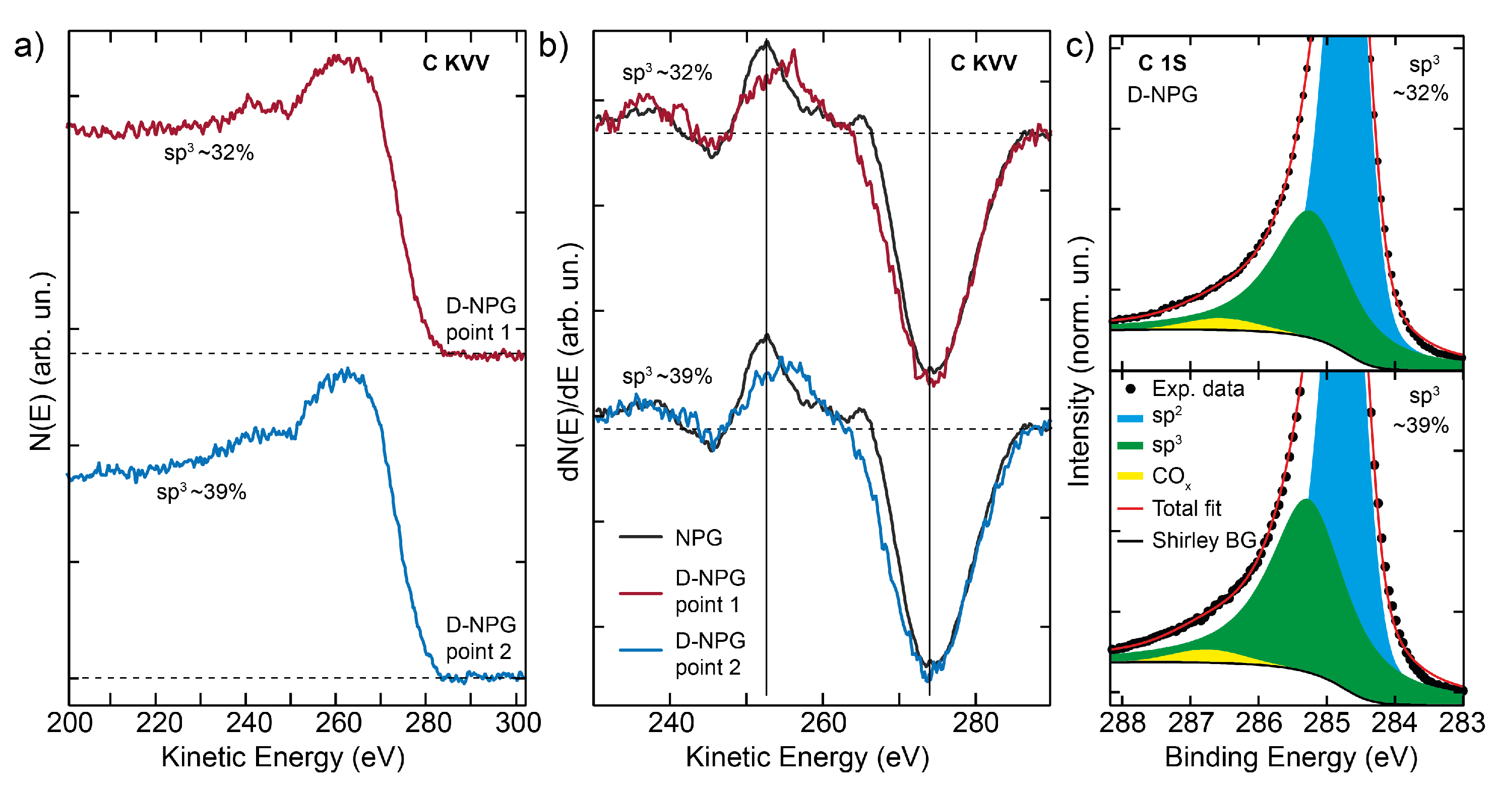
3. Results and Discussion
4. Conclusions
Author Contributions
Funding
Institutional Review Board Statement
Informed Consent Statement
Data Availability Statement
Acknowledgments
Conflicts of Interest
Abbreviations
| XPS | X ray Photoelectron Spectroscopy |
| NPG | Nano Porous Graphene |
| UHV | Ultra High Vacuum |
| 3D | Three Dimensional |
| 2D | Two Dimensional |
References
- Sofo, J.O.; Chaudhari, A.S.; Barber, G.D. Graphane: A two-dimensional hydrocarbon. Phys. Rev. B 2007, 75, 153401. [Google Scholar] [CrossRef] [Green Version]
- Cudazzo, P.; Attaccalite, C.; Tokatly, I.V.; Rubio, A. Strong Charge-Transfer Excitonic Effects and the Bose-Einstein Exciton Condensate in Graphane. Phys. Rev. Lett. 2010, 104, 226804. [Google Scholar] [CrossRef] [PubMed] [Green Version]
- Luo, Z.; Shang, J.; Lim, S.; Li, D.; Xiong, Q.; Shen, Z.; Lin, J.; Yu, T. Modulating the electronic structures of graphene by controllable hydrogenation. Appl. Phys. Lett. 2010, 97, 233111. [Google Scholar] [CrossRef]
- Shkrebtii, A.I.; Heritage, E.; McNelles, P.; Cabellos, J.L.; Mendoza, B.S. Graphene and graphane functionalization with hydrogen: Electronic and optical signatures. Phys. Status Solidi C 2012, 9, 1378–1383. [Google Scholar] [CrossRef]
- Abdelnabi, M.M.S.; Blundo, E.; Betti, M.G.; Cavoto, G.; Placidi, E.; Polimeni, A.; Ruocco, A.; Hu, K.; Ito, Y.; Mariani, C. Towards free-standing graphane: Atomic hydrogen and deuterium bonding to nanoporous graphene. Nanotechnology 2020, 32, 035707. [Google Scholar] [CrossRef]
- Abdelnabi, M.M.S.; Izzo, C.; Blundo, E.; Betti, M.G.; Sbroscia, M.; Di Bella, G.; Cavoto, G.; Polimeni, A.; García-Cortés, I.; Rucandio, I.; et al. Deuterium Adsorption on Free-Standing Graphene. Nanomaterials 2021, 11, 130. [Google Scholar] [CrossRef]
- Betti, M.G.; Placidi, E.; Izzo, C.; Blundo, E.; Polimeni, A.; Sbroscia, M.; Avila, J.; Dudin, P.; Hu, K.; Ito, Y.; et al. Gap Opening in Double-Sided Highly Hydrogenated Free-Standing Graphene. Nano Lett. 2022, 22, 2971–2977. [Google Scholar] [CrossRef]
- Cai, L.; Zhang, Z.; Xiao, H.; Chen, S.; Fu, J. An eco-friendly imprinted polymer based on graphene quantum dots for fluorescent detection of p-nitroaniline. RSC Adv. 2019, 9, 41383–41391. [Google Scholar] [CrossRef] [Green Version]
- Chen, H.; Chen, Z.; Yang, H.; Wen, L.; Yi, Z.; Zhou, Z.; Dai, B.; Zhang, J.; Wu, X.; Wu, P. Multi-mode surface plasmon resonance absorber based on dart-type single-layer graphene. RSC Adv. 2022, 12, 7821–7829. [Google Scholar] [CrossRef]
- Long, F.; Zhang, Z.; Wang, J.; Yan, L.; Zhou, B. Cobalt-nickel bimetallic nanoparticles decorated graphene sensitized imprinted electrochemical sensor for determination of octylphenol. Electrochim. Acta 2015, 168, 337–345. [Google Scholar] [CrossRef]
- Tang, N.; Li, Y.; Chen, F.; Han, Z. In situ fabrication of a direct Z-scheme photocatalyst by immobilizing CdS quantum dots in the channels of graphene-hybridized and supported mesoporous titanium nanocrystals for high photocatalytic performance under visible light. RSC Adv. 2018, 8, 42233–42245. [Google Scholar] [CrossRef] [Green Version]
- Zhang, Z.; Cai, R.; Long, F.; Wang, J. Development and application of tetrabromobisphenol A imprinted electrochemical sensor based on graphene/carbon nanotubes three-dimensional nanocomposites modified carbon electrode. Talanta 2015, 134, 435–442. [Google Scholar] [CrossRef]
- Burgess, J.S.; Matis, B.R.; Robinson, J.T.; Bulat, F.A.; Perkins, F.K.; Houston, B.H.; Baldwin, J.W. Tuning the electronic properties of graphene by hydrogenation in a plasma enhanced chemical vapor deposition reactor. Carbon 2011, 49, 4420–4426. [Google Scholar] [CrossRef]
- Felten, A.; McManus, D.; Rice, C.; Nittler, L.; Pireaux, J.J.; Casiraghi, C. Insight into hydrogenation of graphene: Effect of hydrogen plasma chemistry. Appl. Phys. Lett. 2014, 105, 183104. [Google Scholar] [CrossRef]
- Elias, D.C.; Nair, R.R.; Mohiuddin, T.M.G.; Morozov, S.V.; Blake, P.; Halsall, M.P.; Ferrari, A.C.; Boukhvalov, D.W.; Katsnelson, M.I.; Geim, A.K.; et al. Control of Graphene’s Properties by Reversible Hydrogenation: Evidence for Graphane. Science 2009, 323, 610–613. [Google Scholar] [CrossRef] [Green Version]
- Zhao, F.; Raitses, Y.; Yang, X.; Tan, A.; Tully, C.G. High hydrogen coverage on graphene via low temperature plasma with applied magnetic field. Carbon 2021, 177, 244–251. [Google Scholar] [CrossRef]
- Haberer, D.; Vyalikh, D.V.; Taioli, S.; Dora, B.; Farjam, M.; Fink, J.; Marchenko, D.; Pichler, T.; Ziegler, K.; Simonucci, S.; et al. Tunable Band Gap in Hydrogenated Quasi-Free-Standing Graphene. Nano Lett. 2010, 10, 3360–3366. [Google Scholar] [CrossRef]
- Paris, A.; Verbitskiy, N.; Nefedov, A.; Wang, Y.; Fedorov, A.; Haberer, D.; Oehzelt, M.; Petaccia, L.; Usachov, D.; Vyalikh, D.; et al. Kinetic Isotope Effect in the Hydrogenation and Deuteration of Graphene. Adv. Funct. Mater. 2013, 23, 1628–1635. [Google Scholar] [CrossRef] [Green Version]
- Di Bernardo, I.; Avvisati, G.; Mariani, C.; Motta, N.; Chen, C.; Avila, J.; Asensio, M.C.; Lupi, S.; Ito, Y.; Chen, M.; et al. Two-Dimensional Hallmark of Highly Interconnected Three-Dimensional Nanoporous Graphene. ACS Omega 2017, 2, 3691–3697. [Google Scholar] [CrossRef]
- Di Bernardo, I.; Avvisati, G.; Chen, C.; Avila, J.; Asensio, M.C.; Hu, K.; Ito, Y.; Hines, P.; Lipton-Duffin, J.; Rintoul, L.; et al. Topology and doping effects in three-dimensional nanoporous graphene. Carbon 2018, 131, 258–265. [Google Scholar] [CrossRef] [Green Version]
- Sha, X.; Jackson, B. First-principles study of the structural and energetic properties of H atoms on a graphite (0001) surface. Surf. Sci. 2002, 496, 318–330. [Google Scholar] [CrossRef]
- Ruffieux, P.; Gröning, O.; Bielmann, M.; Mauron, P.; Schlapbach, L.; Gröning, P. Hydrogen adsorption on sp2-bonded carbon: Influence of the local curvature. Phys. Rev. B 2002, 66, 245416. [Google Scholar] [CrossRef] [Green Version]
- Tanabe, Y.; Ito, Y.; Sugawara, K.; Hojo, D.; Koshino, M.; Fujita, T.; Aida, T.; Xu, X.; Huynh, K.K.; Shimotani, H.; et al. Electric Properties of Dirac Fermions Captured into 3D Nanoporous Graphene Networks. Adv. Mater. 2016, 28, 10304–10310. [Google Scholar] [CrossRef] [PubMed]
- Tanabe, Y.; Ito, Y.; Sugawara, K.; Koshino, M.; Kimura, S.; Naito, T.; Johnson, I.; Takahashi, T.; Chen, M. Dirac Fermion Kinetics in 3D Curved Graphene. Adv. Mater. 2020, 32, 2005838. [Google Scholar] [CrossRef] [PubMed]
- Malard, L.; Pimenta, M.; Dresselhaus, G.; Dresselhaus, M. Raman spectroscopy in graphene. Phys. Rep. 2009, 473, 51–87. [Google Scholar] [CrossRef]
- Venezuela, P.; Lazzeri, M.; Mauri, F. Theory of double-resonant Raman spectra in graphene: Intensity and line shape of defect-induced and two-phonon bands. Phys. Rev. B 2011, 84, 035433. [Google Scholar] [CrossRef] [Green Version]
- Eckmann, A.; Felten, A.; Mishchenko, A.; Britnell, L.; Krupke, R.; Novoselov, K.S.; Casiraghi, C. Probing the nature of defects in graphene by Raman spectroscopy. Nano Lett. 2012, 12, 3925–3930. [Google Scholar] [CrossRef] [Green Version]
- Lacovig, P.; Pozzo, M.; Alfe, D.; Vilmercati, P.; Baraldi, A.; Lizzit, S. Growth of dome-shaped carbon nanoislands on Ir (111): The intermediate between carbidic clusters and quasi-free-standing graphene. Phys. Rev. Lett. 2009, 103, 166101. [Google Scholar] [CrossRef] [Green Version]
- D′Acunto, G.; Ripanti, F.; Postorino, P.; Betti, M.G.; Scardamaglia, M.; Bittencourt, C.; Mariani, C. Channelling and induced defects at ion-bombarded aligned multiwall carbon nanotubes. Carbon 2018, 139, 768–775. [Google Scholar] [CrossRef]
- Massimi, L.; Ourdjini, O.; Lafferentz, L.; Koch, M.; Grill, L.; Cavaliere, E.; Gavioli, L.; Cardoso, C.; Prezzi, D.; Molinari, E.; et al. Surface-Assisted Reactions toward Formation of Graphene Nanoribbons on Au(110) Surface. J. Phys. Chem. C 2015, 119, 2427–2437. [Google Scholar] [CrossRef]
- Betti, M.G.; Biasotti, M.; Boscá, A.; Calle, F.; Carabe-Lopez, J.; Cavoto, G.; Chang, C.; Chung, W.; Cocco, A.; Colijn, A.; et al. A design for an electromagnetic filter for precision energy measurements at the tritium endpoint. Prog. Part. Nucl. Phys. 2019, 106, 120–131. [Google Scholar] [CrossRef] [Green Version]
- Betti, M.G.; Biasotti, M.; Boscá, A.; Calle, F.; Canci, N.; Cavoto, G.; Chang, C.; Cocco, A.; Colijn, A.; Conrad, J.; et al. Neutrino physics with the PTOLEMY project: Active neutrino properties and the light sterile case. J. Cosmol. Astropart. Phys. 2019, 2019, 047. [Google Scholar] [CrossRef] [Green Version]
- Ito, Y.; Qiu, H.J.; Fujita, T.; Tanabe, Y.; Tanigaki, K.; Chen, M. Bicontinuous Nanoporous N-doped Graphene for the Oxygen Reduction Reaction. Adv. Mater. 2014, 26, 4145–4150. [Google Scholar] [CrossRef]
- Ito, Y.; Tanabe, Y.; Qiu, H.J.; Sugawara, K.; Heguri, S.; Tu, N.H.; Huynh, K.K.; Fujita, T.; Takahashi, T.; Tanigaki, K.; et al. High-Quality Three-Dimensional Nanoporous Graphene. Angew. Chem. Int. Ed. 2014, 53, 4822–4826. [Google Scholar] [CrossRef]
- Ito, Y.; Cong, W.; Fujita, T.; Tang, Z.; Chen, M. High Catalytic Activity of Nitrogen and Sulfur Co-Doped Nanoporous Graphene in the Hydrogen Evolution Reaction. Angew. Chem. Int. Ed. 2015, 54, 2131–2136. [Google Scholar] [CrossRef]
- Ito, Y.; Tanabe, Y.; Han, J.; Fujita, T.; Tanigaki, K.; Chen, M. Multifunctional Porous Graphene for High-Efficiency Steam Generation by Heat Localization. Adv. Mater. 2015, 27, 4302–4307. [Google Scholar] [CrossRef]
- Ito, Y.; Shen, Y.; Hojo, D.; Itagaki, Y.; Fujita, T.; Chen, L.; Aida, T.; Tang, Z.; Adschiri, T.; Chen, M. Correlation between Chemical Dopants and Topological Defects in Catalytically Active Nanoporous Graphene. Adv. Mater. 2016, 28, 10644–10651. [Google Scholar] [CrossRef]
- Bischler, U.; Bertel, E. Simple source of atomic hydrogen for ultrahigh vacuum applications. J. Vac. Sci. Technol. 1993, 11, 458–460. [Google Scholar] [CrossRef]
- Mohiuddin, T.M.G.; Lombardo, A.; Nair, R.R.; Bonetti, A.; Savini, G.; Jalil, R.; Bonini, N.; Basko, D.M.; Galiotis, C.; Marzari, N.; et al. Uniaxial strain in graphene by Raman spectroscopy: G peak splitting, Grüneisen parameters, and sample orientation. Phys. Rev. B 2009, 79, 205433. [Google Scholar] [CrossRef]
- Ding, F.; Ji, H.; Chen, Y.; Herklotz, A.; Dörr, K.; Mei, Y.; Rastelli, A.; Schmidt, O.G. Stretchable Graphene: A Close Look at Fundamental Parameters through Biaxial Straining. Nano Lett. 2010, 10, 3453. [Google Scholar] [CrossRef]
- Zhang, X.; Qiao, X.F.; Shi, W.; Wu, J.B.; Jiang, D.S.; Tan, P.H. Phonon and Raman scattering of two-dimensional transition metal dicalchogenides from monolayer, multilayer to bulk material. Chem. Soc. Rev. 2015, 44, 2757–2785. [Google Scholar] [CrossRef] [Green Version]
- De Luca, M.; Cartoixà, X.; Martín-Sánchez, J.; López-Suárez, M.; Trotta, R.; Rurali, R.; Zardo, I. New insights in the lattice dynamics of monolayers, bilayers, and trilayers of WSe2 and unambiguous determination of few-layer-flakes’ thickness. 2D Mater. 2020, 7, 025004. [Google Scholar] [CrossRef] [Green Version]
- Zhao, Q.; Frisenda, R.; Gant, P.; Perez de Lara, D.; Munuera, C.; Garcia-Hernandez, M.; Niu, Y.; Wang, T.; Jie, W.; Castellanos-Gomez, A. Toward Air Stability of Thin GaSe Devices: Avoiding Environmental and Laser-Induced Degradation by Encapsulation. Adv. Funct. Mater. 2018, 28, 1805304. [Google Scholar] [CrossRef] [Green Version]
- Niu, Y.; Gonzalez-Abad, S.; Frisenda, R.; Marauhn, P.; Drüppel, M.; Gant, P.; Schmidt, R.; Taghavi, N.S.; Barcons, D.; Molina-Mendoza, A.J.; et al. Thickness-Dependent Differential Reflectance Spectra of Monolayer and Few-Layer MoS2, MoSe2, WS2 and WSe2. Nanomaterials 2018, 8, 725. [Google Scholar] [CrossRef] [Green Version]
- Felton, J.; Blundo, E.; Ling, S.; Glover, J.; Kudrynskyi, Z.R.; Makarovsky, O.; Kovalyuk, Z.D.; Besley, E.; Walker, G.; Polimeni, A.; et al. The Interaction of Hydrogen with the van der Waals Crystal γ-InSe. Molecules 2020, 25, 2526. [Google Scholar] [CrossRef]
- Blundo, E.; Di Giorgio, C.; Pettinari, G.; Yildirim, T.; Felici, M.; Lu, Y.; Bobba, F.; Polimeni, A. Engineered Creation of Periodic Giant, Nonuniform Strains in MoS2 Monolayers. Adv. Mater. Interfaces 2020, 7, 2000621. [Google Scholar] [CrossRef]
- Blundo, E.; Surrente, A.; Spirito, D.; Pettinari, G.; Yildirim, T.; Chavarin, C.A.; Baldassarre, L.; Felici, M.; Polimeni, A. Vibrational Properties in Highly Strained Hexagonal Boron Nitride Bubbles. Nano Lett. 2022, 22, 1525–1533. [Google Scholar] [CrossRef] [PubMed]
- Hornekær, L.; Rauls, E.; Xu, W.; Šljivančanin, Ž.; Otero, R.; Stensgaard, I.; Lægsgaard, E.; Hammer, B.; Besenbacher, F. Clustering of Chemisorbed H(D) Atoms on the Graphite (0001) Surface due to Preferential Sticking. Phys. Rev. Lett. 2006, 97, 186102. [Google Scholar] [CrossRef] [PubMed] [Green Version]
- Boukhvalov, D.W.; Katsnelson, M.I.; Lichtenstein, A.I. Hydrogen on graphene: Electronic structure, total energy, structural distortions and magnetism from first-principles calculations. Phys. Rev. B 2008, 77, 035427. [Google Scholar] [CrossRef] [Green Version]
- Luo, Z.; Yu, T.; Kim, K.-J.; Ni, Z.; You, Y.; Lim, S.; Shen, Z.; Wang, S.; Lin, J. Thickness-Dependent Reversible Hydrogenation of Graphene Layers. ACS Nano 2009, 3, 1781–1788. [Google Scholar] [CrossRef]
- Stankovich, S.; Dikin, D.A.; Piner, R.D.; Kohlhaas, K.A.; Kleinhammes, A.; Jia, Y.; Wu, Y.; Nguyen, S.T.; Ruoff, R.S. Synthesis of graphene-based nanosheets via chemical reduction of exfoliated graphite oxide. Carbon 2007, 45, 1558–1565. [Google Scholar] [CrossRef]
- Shin, Y.E.; Sa, Y.J.; Park, S.; Lee, J.; Shin, K.H.; Joo, S.H.; Ko, H. An ice-templated, pH-tunable self-assembly route to hierarchically porous graphene nanoscroll networks. Nanoscale 2014, 6, 9734–9741. [Google Scholar] [CrossRef]
- Jiménez-Arévalo, N.; Leardini, F.; Ferrer, I.J.; Ares, J.R.; Sánchez, C.; Saad Abdelnabi, M.M.; Betti, M.G.; Mariani, C. Ultrathin Transparent B–C–N Layers Grown on Titanium Substrates with Excellent Electrocatalytic Activity for the Oxygen Evolution Reaction. Acs Appl. Energy Mater. 2020, 3, 1922–1932. [Google Scholar] [CrossRef]
- Barinov, A.; Gregoratti, L.; Dudin, P.; La Rosa, S.; Kiskinova, M. Imaging and Spectroscopy of Multiwalled Carbon Nanotubes during Oxidation: Defects and Oxygen Bonding. Adv. Mater. 2009, 21, 1916–1920. [Google Scholar] [CrossRef]
- Balog, R.; Andersen, M.; Jørgensen, B.; Sljivancanin, Z.; Hammer, B.; Baraldi, A.; Larciprete, R.; Hofmann, P.; Hornekær, L.; Lizzit, S. Controlling Hydrogenation of Graphene on Ir(111). ACS Nano 2013, 7, 3823–3832. [Google Scholar] [CrossRef]
- Scardamaglia, M.; Amati, M.; Llorente, B.; Mudimela, P.; Colomer, J.F.; Ghijsen, J.; Ewels, C.; Snyders, R.; Gregoratti, L.; Bittencourt, C. Nitrogen ion casting on vertically aligned carbon nanotubes: Tip and sidewall chemical modification. Carbon 2014, 77, 319–328. [Google Scholar] [CrossRef]
- Susi, T.; Kaukonen, M.; Havu, P.; Ljungberg, M.P.; Ayala, P.; Kauppinen, E.I. Core level binding energies of functionalized and defective graphene. Beilstein J. Nanotechnol. 2014, 5, 121–132. [Google Scholar] [CrossRef] [Green Version]
- Kozakov, A.; Kochur, A.; Kumar, N.; Panda, K.; Nikolskii, A.; Sidashov, A. Determination of sp2 and sp3 phase fractions on the surface of diamond films from C1s, valence band X-ray photoelectron spectra and CKVV X-ray-excited Auger spectra. Appl. Surf. Sci. 2021, 536, 147807. [Google Scholar] [CrossRef]
- Morgan, D.J. Comments on the XPS Analysis of Carbon Materials. C 2021, 7, 51. [Google Scholar] [CrossRef]


Publisher’s Note: MDPI stays neutral with regard to jurisdictional claims in published maps and institutional affiliations. |
© 2022 by the authors. Licensee MDPI, Basel, Switzerland. This article is an open access article distributed under the terms and conditions of the Creative Commons Attribution (CC BY) license (https://creativecommons.org/licenses/by/4.0/).
Share and Cite
Betti, M.G.; Blundo, E.; De Luca, M.; Felici, M.; Frisenda, R.; Ito, Y.; Jeong, S.; Marchiani, D.; Mariani, C.; Polimeni, A.; et al. Homogeneous Spatial Distribution of Deuterium Chemisorbed on Free-Standing Graphene. Nanomaterials 2022, 12, 2613. https://doi.org/10.3390/nano12152613
Betti MG, Blundo E, De Luca M, Felici M, Frisenda R, Ito Y, Jeong S, Marchiani D, Mariani C, Polimeni A, et al. Homogeneous Spatial Distribution of Deuterium Chemisorbed on Free-Standing Graphene. Nanomaterials. 2022; 12(15):2613. https://doi.org/10.3390/nano12152613
Chicago/Turabian StyleBetti, Maria Grazia, Elena Blundo, Marta De Luca, Marco Felici, Riccardo Frisenda, Yoshikazu Ito, Samuel Jeong, Dario Marchiani, Carlo Mariani, Antonio Polimeni, and et al. 2022. "Homogeneous Spatial Distribution of Deuterium Chemisorbed on Free-Standing Graphene" Nanomaterials 12, no. 15: 2613. https://doi.org/10.3390/nano12152613